行政院國家科學委員會專題研究計畫 成果報告
利用奈米碳管束製作表面傳導電子發射顯示器之研究 研究成果報告(精簡版)
計 畫 類 別 : 個別型
計 畫 編 號 : NSC 98-2221-E-011-021-
執 行 期 間 : 98 年 08 月 01 日至 99 年 10 月 31 日 執 行 單 位 : 國立臺灣科技大學電子工程系
計 畫 主 持 人 : 李奎毅
計畫參與人員: 碩士班研究生-兼任助理人員:陳鏡安 碩士班研究生-兼任助理人員:李冠緯 碩士班研究生-兼任助理人員:粘凱翔
報 告 附 件 : 出席國際會議研究心得報告及發表論文
處 理 方 式 : 本計畫涉及專利或其他智慧財產權,2 年後可公開查詢
中 華 民 國 100 年 02 月 16 日
行政院國家科學委員會補助專題研究計畫 ■ 成 果 報 告
□期中進度報告
利用奈米碳管製作表面傳導電子發射顯示器之研究
計畫類別:
■
個別型計畫 □整合型計畫 計畫編號:NSC 98-2221-E-011-021-執行期間: 2009 年 8 月 1 日至 2010 年 10 月 31 日 執行機構及系所:國立台灣科技大學 電子工程系
計畫主持人:李奎毅 共同主持人:
計畫參與人員:陳鏡安、李冠緯、粘凱翔
成果報告類型(依經費核定清單規定繳交):
■
精簡報告 □完整報告本計畫除繳交成果報告外,另須繳交以下出國心得報告:
□赴國外出差或研習心得報告
□赴大陸地區出差或研習心得報告
■
出席國際學術會議心得報告□國際合作研究計畫國外研究報告
處理方式:除列管計畫及下列情形者外,得立即公開查詢
□涉及專利或其他智慧財產權,□一年□二年後可公開查詢 中 華 民 國 2011 年 1 月 31 日
附件一
中文摘要
傳統的表面傳導電子發射射極是由具有奈米狹縫之氧化鈀薄膜所組成,此奈米狹縫不易製造且加 工複雜。在實際應用上即以施加電壓於氧化鈀薄膜產生穿隧電子與散射電子,此傳統之設計並不易改 善電子發射效率。本計畫以所設計之圖形藉由光微影技術定義於石英基板上,再利用熱化學氣相沉積 法以乙炔為碳源成長高方向性且具有高數密度之奈米碳管陣列取代氧化鈀薄膜來作為新型之表面傳導 電子發射射極。在設計上利用尖端放電的原理,將具有20度尖角之三角星形奈米碳管陣列設計作為放 射陰極,並另以三角形奈米碳管陣列做為陽極,此陽極之三邊皆可同時由陰極發射之電子產生二次電 子。此最佳化之設計不但節省空間並提高了傳導電子發射效率。此外,為了增強奈米碳管陣列的電子 放射特性,我們利用電子束蒸鍍法將氧化鎂奈米結構成長於奈米碳管表面。由實驗結果得到證實,披 覆氧化鎂奈米結構之奈米碳管陣列,可以增強二次電子放射特性並改善電子發射效率,並且得到較佳 之放射電流。本計畫成功地將奈米碳管陣列應用於表面傳導電子發射顯示器上其研究成果可提供相關 顯示器產業之參考。
關鍵字: 表面傳導電子發射顯示器,奈米碳管,二次電子,場電子發射,熱化學氣相沉積法,氧化鎂
英文摘要
The traditional surface-conduction electron-emitter (SCE) consists of the palladium oxide (PdO) film with a nanogap. The manufacture of a nanogap is quite difficult and complex. The electrons can be emitted by applying a voltage to the PdO film and scattered on the PdO film. It is not easy to improve the electron emission efficiency of the traditional SCE type. In this project, a new design pattern was defined on quartz substrates by photolithography. The vertically aligned carbon nanotube (VACNT) bundle arrays were synthesized on the quartz substrates using a thermal chemical vapor deposition (TCVD) system. C2H2 gas was used as the carbon source. The VACNT bundle array was used to replace the PdO film. The delta-star shaped VACNT arrays with three 20o tips as the cathodes emitted the electrons easily due to the high electrical field gradient. Moreover, to enhance the electron emission characteristics of the VACNTs bundle arrays, the magnesium oxide (MgO) nanostructures were coated on the VACNT arrays using electron beam evaporation.
The experimental results showed a relative higher emission current was obtained after the MgO coating. The MgO nanostructure coated on the VACNT bundle arrays could improve the secondary electron emission characteristic and the electron emission efficiency. The successful type of this project result can provide a promising application on display industry.
Keyword: Surface-conduction electron-emitter display,Carbon nanotube, Secondary electron, Field emission, Thermal chemical vapor deposition, MgO
報告內容
前言、目的、文獻探討
In recent years, cathode ray tubes (CRTs) have been gradually replaced by flat panel displays (FPD).
There are several types of display products in the FPD market, such as liquid crystal displays (LCDs), plasma display panels (PDPs), organic light-emitting diodes (OLEDs), and field emission displays (FEDs). Because FEDs offer low power consumption, high luminance, low reaction time, and high visual angle, they are considered an important next-generation display product [1,2].
Surface-conduction electron-emitter display (SED) is an emerging display technology that, like the FED, has several of the attractive characteristics of the CRT. The SED has a simple device structure consisting of surface conduction electron emitters (SCEs) and a high-voltage anode.
Traditional SCE consists of the palladium oxide (PdO) film with a nanogap. The electrons can be emitted by applying a voltage to the PdO film and scattered on the PdO film. Although the nanogap is a crucial part of SCE, the manufacture of a nanogap is quite difficult and complex. To simplify the process and improve the electron emission efficiency, the PdO film is replaced by the vertically aligned carbon nanotube (VACNT) arrays.
In this study, the delta-star shaped CNT arrays with 20o tips as the cathodes emitted the electron easily due to the high electrical field gradient. To enhance the electron emission characteristics of the CNTs arrays, the magnesium oxide (MgO) nanostructures were coated on the CNT arrays using electron beam evaporation. The secondary electron emission characteristics of MgO-coated CNT arrays were investigated. The experimental results showed the emission current of 0.13 mA was obtained from the 10 nm-MgO-coated CNT arrays. The MgO nanostructure coated on the CNT arrays could improve the secondary electron emission characteristic.
The SCEs based on the MgO-coated CNT arrays promise application in the surface-conduction electron-emitter displays in the near future.
研究方法
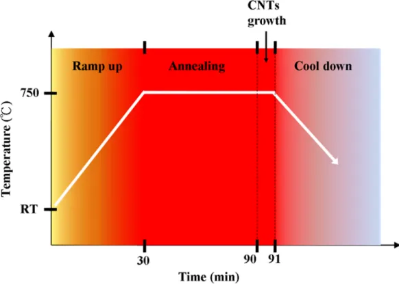
The substrate used for VACNT bundle arrays formation was the quartz. The design pattern of VACNT arrays was defined onto quartz substrates using photolithography. A set of SCE consisted of a delta-star array with three 20o tips as a cathode emitter and three equilateral-triangle arrays as anode receivers. The gap between the cathode tip and opposite anode side was 50 μm. An Al film (5 nm) as the buffer layer and Fe film (3 nm) as the catalyst metal were deposited by e-beam evaporator. Subsequently, for the Fe catalyst nanoparticle formation, the samples were place into a thermal chemical vapor deposition (TCVD) system and were annealed at 750oC under a base pressure of 2 × 10⁻² Torr for 60 min. After annealing, C2H2 gas as the carbon source was introduced into the TCVD system under a pressure of 2 Torr. The VACNT growth time was 1 min. Figure 1 shows the procedure of VACNT bundle arrays growth.
MgO nanostructures were deposited on the surface of VACNT bundle arrays using electron-beam (e-beam) evaporation. The e-beam system chamber was evacuated to a base pressure of about 8×10⁻⁷ Torr, and the samples were heated up to 300oC. The MgO granule (99.99%) was used as a MgO source. The MgO nanostructures were coated on the surface of samples at the deposition rate ranged between 0.1 and 0.3 Å/sec in the O2 gas flow of 2 sccm. The experimental sequence was shown in Fig. 2.
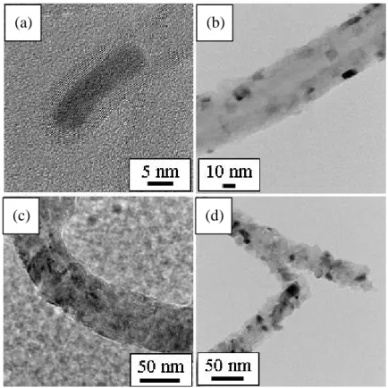
The surface morphology of the formed nanostructure was observed by scanning electron microscopy (SEM). The internal structures of pristine CNTs and MgO-coated CNTs were observed by using transmission electron microscopy (TEM). X-ray photoelectron spectroscopy (XPS), known as electron spectroscopy for chemical analysis (ESCA), was used to observe chemical bonding of the surface. X-ray diffraction (XRD) determined the crystallographic structure of the samples. The electrical properties of formed VACNT bundle
arrays were measured in a homemade high-vacuum secondary electron emission (SEE) measurement system consisting of a stainless steel chamber, two sets of high-voltage source meters.
結果與討論
The VACNTs were successfully synthesized with design geometrical structures on quartz substrates. Fig.
3(a) The geometrical structure of pristine CNT arrays, where the spacing between the anode and cathode electrodes was 50 μm which is identical to the design mask. The angle of the VACNT cathode tips was 20o, as shown in Fig. 3(b). Fig. 3(c) shows an enlarged SEM image of the side-view of the synthesized VACNTs. The length of VACNTs was about 15 μm long, and presented in a high number-density of approximately 109 cm-2. In this project deposited the MgO nanostructures on the pristine VACNT bundle arrays to enhance the characteristics of field emission (FE) and secondary electron emission (SEE). After MgO-deposition, the VACNT bundle arrays still maintained their shape with three tips of 20o. Figs. 3(d)-3(f) show the SEM images of the VACNT bundle arrays deposited with different MgO layers measuring 5, 10, and 20 nm thick, respectively. It is obvious that the MgO nanostructures were coated uniformly on the surface of VACNT bundle arrays. Figure 4(a) shows the TEM images of the pristine VACNT. A hollow tubular and multi-walled structure could be observed. A catalyst nanoparticle was found at the tip of the CNT, indicating that the CNTs were formed in the tip- growth mode. Figs. 4(b)-4(d) shows CNTs coated uniformly with different thicknesses of 5, 10, and 20 nm MgO nanostructures, respectively.
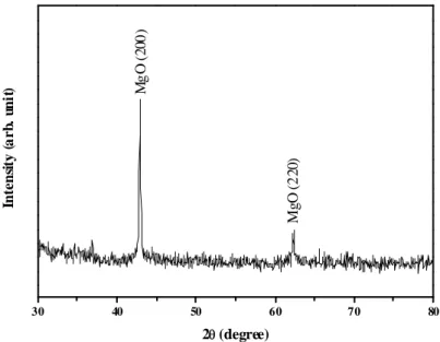
Fig. 5 shows the XRD result of the MgO-coated VACNTs. The spectral peaks occured at 2θ = 42.9o and 62.4o, which corresponded to the planes ((200) and (220)) of MgO [3,4]. The formed MgO nanostructure on VACNTs exhibited a preferred (200) orientation and revealed a well agreement with MgO. Fig. 6 shows the XPS spectra of the MgO nanostructures deposited on the surface of VACNTs. Fig. 6(a) shows the C 1s core level spectrum of the MgO-coated VACNTs. The C 1s spectrum of MgO-coated VACNTs shows a main peak at 284.5 eV, which corresponds to the sp2-hybridized carbon [5]. The peak occurs at 289 eV was attributed to the Mg-C bond formation [6]. The Mg 2p core level spectrum of the MgO-coated VACNTs after atmosphere exposure was shown in Fig. 6(b). In this figure, there were two peaks at 48.9 and 49.7 resolved in the Mg 2p spectrum. They represented the MgO and magnesium hydroxide formation, respectively [7].
The experiments in this study synthesized a CNT array consisting of two electrodes on a quartz substrate.
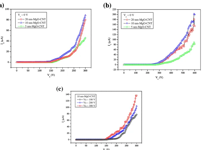
Fig. 7 shows that the geometrical structure of the CNT arrays created SCEs. The CNT electrode with a delta-star shape is the cathode, while those with equilateral triangles are anodes. The three tips of the middle delta-star function as field emitters. Fig. 8(a) shows the tunneling effect of 100 sets of MgO-coated VACNT bundle arrays. When Va was applied to 0 V, the tunneling voltage was 146 V for 10 nm-MgO-coated VACNT bundle arrays. This value was lower than that of 5 and 20 nm-MgO-coated VACNT bundle arrays. Fig. 8(b) shows the FE properties of 100 sets of MgO-coated VACNT bundle arrays. The threshold voltage (Vth) was defined as a applied for the FE 10 μA. The 10 nm-MgO-coated VACNT bundle arrays also had a relatively lower Vth. When the operation voltage Va was applied to be 300 V, the 10 nm-MgO-coated VACNT bundle arrays exhibited the relatively higher FE current. This maybe due to that the high FE current was attributed to the SEE yield from the MgO-coating layer. It is obvious that the 5 nm-MgO-coated VACNT bundle arrays had a relatively lower FE current than that of the other MgO-coated VACNT bundle arrays because of the small escape depth of the thin MgO-coating layer. When the thickness of MgO coating increased, the SEE yield increased with an increase of escape depth. However, when the thickness of MgO coating exceeded the penetration depth of primary electron, the SEE yield decreased due to the surface charge accumulation on the MgO layer. The MgO layer suffered from providing electrons from the MgO/CNT interface to the electron-emitting surface during the SEE process. The 10 nm-MgO-coating layer achieved a high SEE yield
due to its large escape depth and the continuous electron supplying from the CNT. Therefore, the 10 nm-MgO-coated CNT arrays generated a relatively higher emission current due to the high tunneling current and the high SEE yield. It was reported that the mechanisms of electron supply determined the magnitude of the SEE yield of MgO film [12]. Therefore, in this study, due to the high tunneling current and the high SEE yield, the 10 nm thickness of MgO coating produced a relatively higher FE current. In Fig. 8(c), the 10 nm MgO-coated VACNT bundle arrays could reach 137 μA at Va of 400 V and Vg of 300 V.
In this project, the VACNT bundle arrays were designed and successfully synthesized as the SCEs to be applied to SED. To enhance the FE current and the SEE yield characteristics, the VACNT bundle arrays were coated with MgO nanostructures by e-beam evaporation. The results showed that the 100 sets of 10 nm-MgO-coated VACNT bundle arrays could reached 137 μA at Va of 400 V and Vg of 300 V. The results showed that the new configuration of SED could provide a new design idea for the SED application.
參考文獻
[1] Y. S. Choi, “Shapes of emitter surface in field emission display,” Thin Solid Films, vol. 516, pp.
3357-3363, 2008.
[2] J.-L. Kwo, M. Yokoyama, and I.-N. Lin, “Effects of composition on field emission character of tetrahedral amorphous carbon,” Appl. Surf. Sci., vol. 142, pp. 521-526, 1999.
[3] Z.-N. Yu, J.-W. Seo, D.-X. Zheng, and J. Sun, “Structural and discharging properties of MgO thin films prepared by ion beam-assisted deposition,” Surf. Coat. Technol., vol. 163-164, pp. 398-404, 2003.
[4] Y. Yan, L. Zhou, and Y. Zhang, “Synthesis of MgO hierarchical nanostructures controlled by the supersaturation ratio,” J. Phys. Chem. C, vol. 112, pp. 19831-19835, 2008.
[5] T. V. Sreekumar, T. Liu, and S. Kumar, ”Single-wall carbon nanotube films,” Chem. Mater., vol. 15, pp.
175-178, 2003.
[6] D. K. Aswal, K. P. Muthe, S. Tawde, S. Chodhury, N. Bagkar, A. Singh, S. K. Gupta, and J. V. Yakhimi,
“XPS and AFM investigations of annealing induced surface modifications of MgO single crystals,” J.
Cryst. Growth, vol. 236, pp. 661-666, 2002.
[7] H. B. Yao, Y. Li, and A. T. S. Wee, “An XPS investigation of the oxidationrcorrosion of melt-spun Mg,”
Appl. Surf. Sci., vol. 158, pp. 112-119, 2000.
[8] D. Caceres, I. Colera, I. Vergara, R. Gonzalez, and E. Roman, “Characterization of MgO thin films grown by rf-sputtering,” Vacuum, vol. 67, pp. 577-581, 2002.
[9] P. Casey, E. OConnor, R. Long, B. Brennan, S.A. Krasnikov, D. OConnell, P. K. Hurley, and G. Hughes,
“Growth, ambient stability and electrical characterisation of MgO thin films on silicon surfaces,”
Microelectron. Eng., vol. 86, pp. 1711-1714, 2009.
[10] C. Xu and D. W. Goodman, “Structure and geometry of water adsorbed on the MgO(100) surface,”
Chem. Phys. Lett., vol. 265, pp. 341-346, 1997.
[11] S. H. Moon, T. W. Heo, S. Y. Park, J. H. Kim, and H. J. Kim, “The effect of the dehydration of MgO films on their XPS spectra and electrical properties,” J. Electrochem. Soc., vol. 154, pp. J408-J412, 2007.
[12] J. Lee, T. Jeong, S. Yu, S. Jin, J. Heo, W. Yi, D. Jeon, and J. M. Kim, “Thickness effect on secondary electron emission of MgO layers,” Appl. Surf. Sci., vol. 174, pp.62-69, 2001.
Figure 1. The curve of temperature versus time for VACNTs growth.
Figure 2. The curve of temperature versus time for MgO nanostructure evaporation.
Figure 3. SEM images of pristine and MgO-coated CNTs on quartz substrate. (a) The geometrical structure of pristine CNT arrays. (b) The SCE cathode. (c) The side view of pristine CNTs. (d) The CNTs coated by 5 nm thick MgO nanostructure. (e) The CNTs coated by 10 nm thick MgO nanostructure. (f) The CNTs coated by 20 nm thick MgO nanostructure.
Figure 4. SEM images of pristine and MgO-coated CNTs on quartz substrate. (a) The tip of pristine CNT. (b) The CNTs coated by 5 nm thick MgO nanostructure. (c) The CNTs coated by 10 nm thick MgO nanostructure.
(d) The CNTs coated by 20 nm thick MgO nanostructure.
(d) (a)
(c)
(b)
Figure 5. The XRD pattern of the MgO-coated vertically aligned CNTs.
Figure 6. The XPS spectra of MgO-coated CNTs after atmosphere exposure. The (a) C 1s and (b) Mg 2p core level spectrum.
Figure 7. A schematic of geometrical structure of a CNT array.
30 40 50 60 70 80
MgO (220)
Intensity (arb. unit)
2θ (degree)
MgO (200)
0 50 100 150 200 250 300 0
20 40 60 80 100
Ig (μA)
Vg (V) Va = 0 V
20 nm-MgO-CNT 10 nm-MgO-CNT 5 nm-MgO-CNT
(a)
0 50 100 150 200 250 300
0 20 40 60 80 100
Ig (μA)
Vg (V) Va = 0 V
20 nm-MgO-CNT 10 nm-MgO-CNT 5 nm-MgO-CNT
(a)
0 100 200 300 400 500 600
-20 0 20 40 60 80 100 120 140 160 180 200 220
Ia (μA)
Va (V) Vg = 0 V
20 nm-MgO-CNT 10 nm-MgO-CNT 5 nm-MgO-CNT
(b)
0 100 200 300 400 500 600
-20 0 20 40 60 80 100 120 140 160 180 200 220
Ia (μA)
Va (V) Vg = 0 V
20 nm-MgO-CNT 10 nm-MgO-CNT 5 nm-MgO-CNT
(b)
Figure 8. The I-V characteristics of MgO-coated CNT arrays. (a) The current Ig versus voltage Vg curves. (b) The current Ia versus voltage Va curves. (c) The electron emission characteristics of 10 nm MgO-coated CNT arrays.
0 50 100 150 200 250 300
0 20 40 60 80 100 120 140
Ia (μA)
Vg (V) 10 nm-MgO-CNT
Va = 100 V Va = 200 V Va = 300 V
(d)
0 50 100 150 200 250 300
0 20 40 60 80 100 120 140
Ia (μA)
Vg (V) 10 nm-MgO-CNT
Va = 100 V Va = 200 V Va = 300 V
(c) (d)
1
國科會補助專題研究計畫項下出席國際學術會議心得報告
日期:2009 年 11 月 19 日
參加會議經過:
2009 年 微 製 程 及 奈 米 科 技 國 際 研 討 會 (2009 International Microprocesses and Nanotechnology Conference, MNC2009)於 2009 年 11 月 16 日至 19 日於日本札幌 Sheraton Sapporo Hotel 國際會議中心 舉行。會議主辦單位為國際純粹及應用聯合物理學會(International Union of Pure and Applied Physics)。
本研討會的主要宗旨在於發表最新的微奈米處理製程及奈米技術,包括材料特性、製程及分析。本屆 大會除了日本外,臺灣、美國、瑞士、英國、愛爾蘭、法國、韓國等國共約發表二百六十篇論文(oral and poster presentations)。其發表之研究學者及團體除一般學校及研究所單位外亦有著名公司及廠商發表。
參展的廠商也提供最新研發之奈米相關製程及量測儀器。近年,由於在低維度系統及奈米科技相關領 域之研究非常蓬勃,許多跨領域之科學及工程技術之新發現相當受到注目。許多新的奈米材料及相關 合成技術、精密量測等研究主題在本會議中受到相當熱烈的討論。本會議之主辦單位在會前之 Technical Seminar 安排了奈米科技及生物相關領域方面的結合研究發表,希望能提供更多元化的合作及跨領域的 開拓。
這次發表的論文為摻氮二氧化鈦奈米結構物質在場電子發射領域之研究,以 poster 發表。本研究 之發表內容主要分為:一、所開發之簡單二氧化鈦奈米結構製程,二、二氧化鈦奈米結構之摻氮過程及
計畫編號 NSC 98-2221-E-011-021-
計畫名稱 利用奈米碳管製作表面傳導電子發射顯示器之研究 出國人員
姓名 李奎毅 服務機構
及職稱 國立台灣科技大學電子系副教授
會議時間
2009 年 11 月 16 日至
2009 年 11 月 19 日
會議地點
日本札幌
會議名稱
(中文)2009 國際微製程及奈米科技會議
(英文)2009 International Microprocesses and Nanotechnology Conference
發表論文 題目
(中文) 不同成分之摻氮二氧化鈦奈米結構之場電子發射特性
(英文) Field Emission Characteristics of TiO2 Nanostructures with Various Nitrogen-Doping Contents
附件四
2
其基本特性之量測,三、改善二氧化鈦奈米結構之場電子發射特性。由於二氧化鈦奈米結構在許多應 用上頗為重要,因此在論文發表時除了在場電子發射上之討論外,在相關的製程及量測方式亦多有建 議及詢問,從中獲取不少新穎的想法,許多有趣的新實驗架構也因此產生。另外,在較熱門的太陽能 電池應用上,二氧化鈦為其中之一可應用之材料。因此,此應用部分也與許多相關研究人員進行熱烈 之討論與交流,收穫良多。在其他研究人員或團體的發表上,亦對其研究領域及實驗結果進行討論,
並收集相關材料特性應用之研究情形,做為未來進行相關研究之參考。相信這些意見及想法必會對未 來之研究規劃有正面之影響。
與會心得:
本國際研討會,在正式發表論文前的 Technical Seminar 是個非常成功的安排。MNC2009 提出一個 在近期內較熱門的主題並請相關的資深研究人員做一個有系統的發表。這個 Technical Seminar 的發表 可使相關的研究人員特別是學生得到一個較完整的概念。此部分不但說明了相關研究的來龍去脈且提 出一些未來的展望。對於此領域不是太熟悉的研究人員亦可在較短的時間內有個大致的瞭解,提供了 一個機會讓不同領域之研究人員進行討論。對想要跨進此新領域的研究人員可評估自身之研究環境與 條件。在正式的論文發表中這些在 Technical Seminar 發表的研究人員亦提出其最先端之成果,除了可 提供一個專業的詢問平台,對許多不同的想法在不同的專業研究背景可引伸出有趣內容,相信不僅是 對學術界,對相關的工業應用必助益良多。雖然許多會議也有類似此 Technical Seminar 的部分,但有 些會議是以拼湊的方式完成,其成效自然大打折扣。
在本次會議中,除了學術單位的發表之外,相關研究領域的廠商亦有展示其研究實驗器材的攤位。
國內的研討會雖然也有參展的部分,但受限於本身研發的經費及能力,絕大部分是將外國的儀器直接 或是代工品展出。而在日本的研討會上除了某些知名的大廠展出外,有許多中小型的廠商也展示其研 發儀器,充分展現其研發能力。其銷售人員亦積極找尋目前其他研究之需求以作為其新的研發目標。
不管廠商的大小,其研發展示人員皆可與會場研究人員面對面的討論問題,甚至以其儀器所做出之結 果於研討會中發表。雖然商業上的利益是主要目標,但所展現出的研發能力令人讚嘆。此部分可使得 參與發表的學生瞭解未來畢業後工作的方向與目標。
本人非常感謝國家科學委員會的補助,能夠參加這次 MNC2009 國際會議並發表論文。在許多研 究問題的討論上得到不少意見,新的想法也孕育而生,相信所獲得的部分對未來之實驗及研究會有實 質的幫助。
攜回資料名稱及內容:
MNC 2009 Digest of 22nd International Microprocesses and Nanotechnology Conference。
其他
附上發表論文之摘要。
3
Field emission characteristics of TiO2 nanostructures with various nitrogen-doping contents K.-Y. Lee1,2, J.-H. Cai2, K.-S. Nian2
1Graduate Institute of Electro-Optical Engineering, National Taiwan University of Science and Technology, Taiwan
2Department of Electronic Engineering, National Taiwan University of Science and Technology, Taiwan Phone: +886-2-2730-1254, Fax: +886-2-2737-6424, E-mail: [email protected]
Recently, TiO2 with various structures has been using in many application fields widely. TiO2 has chemical and thermal stability, but the high electron affinity confines the application of electron field emission (FE). It is reported that the nitrogen doping can improve the FE of TiO2 nanotube array because of the coexistence of nitrogen and oxygen vacancies in TiO2 nanostructures [1]. On the other hand, synthesis of TiO2 nanostructures often needs complicated methods such as anodization, electrochemical, chemical vapor deposition, and thermal evaporation methods [2]. Here we introduce a simple method to directly grow TiO2 nanostructures on Ti sheet and examine the characteristics of the electron FE of TiO2 nanostructures with various content of nitrogen. The N-doping can improve the FE of TiO2 nanostructure.
TiO2 nanostructures were synthesized on a Ti sheet by annealing in atmosphere in a furnace at 700℃ Before . the TiO2 nanostructure formation, Al and Fe films were deposited on the Ti sheet by using e-beam evaporation to define the growth area of TiO2 nanostructures. N-doping TiO2 nanostructures were synthesized with NH3 gas and atmosphere during annealing. The N content in TiO2 nanostructures was controlled by the pressure of NH3 during annealing. The size of the TiO2 nanostructures was controlled by the annealing time. The surface morphologies of the synthesized samples were observed by scanning electron microscopy (SEM). Raman scattering was carried out to investigate the microstructure of TiO2. X-ray photoelectron spectroscopy (XPS) was carried out to determine the nitrogen content. The crystal structures of the samples were examined by X-ray diffraction (XRD). The photoluminescence (PL) spectrum was used to character the optical properties of the samples. The FE characteristics were measured in a high-vacuum system consisted of parallel plates.
Fig. 1 shows the SEM images that the TiO2 nanostructures were grown uniformly on the Ti sheets with and without N-doping. The uneven morphology of TiO2 nanostructures was synthesized. The size of the TiO2
nanostructure increased with the increasing annealing time. The XPS result shows that the nitrogen content in TiO2
nanostructures could not increase unlimitedly with increasing the annealing time. The Raman spectrum (Fig. 2) confirms that the nanostructure was TiO2. The FE characteristic (Fig. 3) was improved obviously by doping nitrogen into the TiO2 nanostructures. However, when the nitrogen content exceeds a specific value, the FE property of the TiO2 nanostructure could not be more enhanced. The long-term stability of FE was measured to show that the stable FE characteristic make the TiO2 nanostructures with N-doping can be used as a field emitter.
Our method provides a promising approach to enhance the FE of TiO2.
REFERENCES
[1] G. Liu, F. Li, D.-W. Wang, D.-M. Tang, C. Liu, X. Ma, G. Q. Lu, and H.-M. Cheng, Nanotechnology 19, 025606 (2008).
[2] J.-M. Wu, H. C. Shih, and W.-T. Wu, Chem. Phys. Lett. 413, 490 (2005).
4
0 200 400 600 800 1000
Intensity (a.u.)
Raman shift (cm-1)
2 3 4 5 6 7
10-6 10-5 10-4 10-3 10-2 10-1 100
J (mA/cm2 )
E (V/μm) TiO2 nanostructures after annealing Pristine TiO
2 nanostructures
Fig. 1 SEM images of TiO2 nanostructures grown on Ti sheet (a) pristine TiO2 nanostructures, (b) after NH3 annealing.
Fig. 3 Field emission characteristic (J-E curve) of TiO2 nanostructures grown on Ti sheet with and without NH3 annealing.
Fig. 2 Raman spectrum of TiO2 nanostructures.
1 μm 1 μm
(a) (b)
國科會補助計畫衍生研發成果推廣資料表
日期:2011/02/14
國科會補助計畫
計畫名稱: 利用奈米碳管束製作表面傳導電子發射顯示器之研究 計畫主持人: 李奎毅
計畫編號: 98-2221-E-011-021- 學門領域: 顯示技術
無研發成果推廣資料
98 年度專題研究計畫研究成果彙整表
計畫主持人:李奎毅 計畫編號:98-2221-E-011-021- 計畫名稱:利用奈米碳管束製作表面傳導電子發射顯示器之研究
量化
成果項目 實際已達成
數(被接受 或已發表)
預期總達成 數(含實際已
達成數)
本計畫實 際貢獻百
分比
單位
備 註 ( 質 化 說 明:如 數 個 計 畫 共 同 成 果、成 果 列 為 該 期 刊 之 封 面 故 事 ...
等)
期刊論文 0 0 100%
研究報告/技術報告 1 1 100%
研討會論文 1 1 100%
論文著作 篇
專書 0 0 100%
申請中件數 0 0 100%
專利 已獲得件數 0 0 100% 件
件數 0 0 100% 件
技術移轉
權利金 0 0 100% 千元
碩士生 3 3 100%
博士生 0 0 100%
博士後研究員 0 0 100%
國內
參與計畫人力
(本國籍)
專任助理 0 0 100%
人次
期刊論文 0 2 100%
研究報告/技術報告 0 1 100%
研討會論文 1 1 100%
論文著作 篇
專書 0 0 100% 章/本
申請中件數 0 0 100%
專利 已獲得件數 0 0 100% 件
件數 0 0 100% 件
技術移轉
權利金 0 0 100% 千元
碩士生 0 0 100%
博士生 0 0 100%
博士後研究員 0 0 100%
國外
參與計畫人力
(外國籍)
專任助理 0 0 100%
人次
其他成果
(無法以量化表達之成
果如辦理學術活動、獲 得獎項、重要國際合 作、研究成果國際影響 力及其他協助產業技 術發展之具體效益事 項等,請以文字敘述填 列。)
無
成果項目 量化 名稱或內容性質簡述
測驗工具(含質性與量性) 0
課程/模組 0
電腦及網路系統或工具 0
教材 0
舉辦之活動/競賽 0
研討會/工作坊 0
電子報、網站 0
科 教 處 計 畫 加 填 項
目 計畫成果推廣之參與(閱聽)人數 0
國科會補助專題研究計畫成果報告自評表
請就研究內容與原計畫相符程度、達成預期目標情況、研究成果之學術或應用價 值(簡要敘述成果所代表之意義、價值、影響或進一步發展之可能性)、是否適 合在學術期刊發表或申請專利、主要發現或其他有關價值等,作一綜合評估。
1. 請就研究內容與原計畫相符程度、達成預期目標情況作一綜合評估
■達成目標
□未達成目標(請說明,以 100 字為限)
□實驗失敗
□因故實驗中斷
□其他原因 說明:
2. 研究成果在學術期刊發表或申請專利等情形:
論文:□已發表 □未發表之文稿 ■撰寫中 □無 專利:□已獲得 □申請中 ■無
技轉:□已技轉 ■洽談中 □無 其他:(以 100 字為限)
專利申請準備中。
3. 請依學術成就、技術創新、社會影響等方面,評估研究成果之學術或應用價 值(簡要敘述成果所代表之意義、價值、影響或進一步發展之可能性)(以 500 字為限)
本計畫之實驗成果改善了傳統的表面傳導電子發射顯示器陰極結構。由於傳統之具有奈米 狹縫之氧化鈀薄膜所組成之陰極其奈米狹縫不易製造,因此在電子之發射效率上大打折 扣。本計畫以所設計之圖形藉由光微影技術定義於石英基板上,再利用熱化學氣相沉積法 以乙炔為碳源成長高方向性且具有高數密度之奈米碳管陣列。此部分確立了高數密度及高 方向性之奈米碳管於石英基板上之成長條件並整理為一資料庫。在陰極之設計上利用亦成 功地成長具有 20 度尖角之三角星形奈米碳管陣列作為放射陰極。此最佳化之設計不但節 省空間並提高了傳導電子發射效率。此外,為了增強奈米碳管陣列的電子放射特性,我們 利用電子束蒸鍍法將氧化鎂奈米結構於奈米碳管表面。在此部分之製程技術上我們也成功 地蒸鍍上均勻之奈米氧化鎂結構。並由實驗結果得到證實,披覆氧化鎂奈米結構之奈米碳 管陣列,可以增強二次電子放射特性並改善電子發射效率,並且得到較佳之放射電流。本 計畫成功地將奈米碳管陣列應用於表面傳導電子發射顯示器上其研究成果可提供相關顯 示器產業之參考。