Theoretical and experimental studies for nano-oxidation of silicon wafer
by ac atomic force microscopy
Jen Fin Lin,a兲Chih Kuang Tai, and Shuan Li Lin
Department of Mechanical Engineering, National Cheng Kung University, Tainan 700, Taiwan, Republic of China
共Received 6 January 2006; accepted 19 January 2006; published online 14 March 2006兲
In the present study, all the oxidational experiments were carried out by using the function of the electrochemical chemical atomic force microscopy. The theory for the growth rate of the oxide film thickness is derived to be the combined effect of the alternating current共ac兲 voltage applied to the system and the charges entrapped in the oxide film formed on silicon wafer. Part of the space charges that accumulated in the oxide film can be removed by the negative part of the ac voltage. The residual proportion of the space charges was first determined by the force-displacement curves obtained from the experiments of the kelvin force microscopy. Then, the formula for the growth rate of the oxide film thickness was slightly modified by weighting this residual proportion at the term related to the space charges. The comparisons between the theoretical and experimental results in the oxide height as a function of different controlling factors were made. The behavior exhibited in the experimental results of the oxide height due to the change in the oxidation time is quite consistent with that predicted by the present model if the applied voltage is not high enough to oxidize the probe. The height of the oxide film was generally increased by elevating the positive electrical voltage. The increase in the modulation number共or the applied voltage frequency兲 was within a fixed time period of the oxide height. © 2006 American Institute of Physics.
关DOI:10.1063/1.2174721兴
I. INTRODUCTION
Scanning probe microscopy共SPM兲 has demonstrated a good potential in the field of nanolithography. The SPM-based techniques have been reported to create nanometer-scale structures on different surfaces. The strong activity de-veloped around this lithography technique takes advantage of the simplicity to reach nanometer range and to visualize the corresponding patterns with the same equipment.
Since the work of Dagata et al.1showing the possibility of generating an oxide pattern with a scanning tunneling mi-croscope operating in air, several research groups have car-ried out the oxidation of silicon surfaces using a scanning tunneling microscope共STM兲.2–9Similar oxidation processes have been reported using an atomic force microscope共AFM兲 with a conducting probe in contact10–16 and noncontact models.17–20 An AFM with a conducting tip biased nega-tively with respect to the sample was applied to induce oxidation.1,12,13,21,22 With this approach, thicker insulating oxides can be produced. Oxide lines as narrow as 10 nm have been generated.13
Several contributors have reported on the mechanism and kinetics of SPM-based oxidation23–26 in order to get a better control and more detailed insight of this patterning method. These methods require the field-induced formation of a liquid bridge. Several experiments have already outlined the influence of the oxidation time on the oxide height.25,27 Some experiments have shown a voltage modulation dependence.28,29 Voltage modulation has been linked to a
space-charge buildup process.24 The liquid bridge size also influences the lateral dimensions of the oxide.20The buildup of space charge within the growing oxide places a rather severe constraint on our ability to favorably influence the kinetics of SPM oxidation. Voltage modulation allows the concentrations of ionic species that would otherwise build up within the oxide film to be reset to an initial value on each cycle.24 Voltage modulation leads to a significant enhance-ment of the growth rate and to an improveenhance-ment in the aspect ratio compared with static voltage pulses. Calleja and Garćia30studied the voltage and pulse duration conditions in order to generate a given height with the minimum lateral size. They found that the combination of short pulses and relatively high voltages produces the highest height-width ratio.
The dependence of the tip-induced oxidation on tip bias provides evidence that the process is affected by the gener-ated electric field. Gordon et al.16 suggested that the initial density of surface OH groups is rate limiting. In the study of Avouris et al.,25 local oxidation of silicon was induced by a strong potential in the use of an AFM. The kinetics and mechanism and how such factors as the strength of the elec-tric field, ambient humidity, and the thickness of the oxide affect its rate and resolution were examined. The fact that water from the ambient is necessary for oxidation had been interpreted by Sugimura et al.,31whose process is analogous to electrochemical anodization.
Teuschler et al.15 attempted to explain the tip-induced oxidation in terms of the Cabrera and Mott model32of field-induced oxidation, although this attempt was unsuccessful. Stiévenard et al.23 proposed an analytical model to explain a兲Author to whom correspondence should be addressed; electronic mail:
quantitatively the variation of the oxide height with the po-larization and the speed of the tip with a model based on field-induced oxidation. The study of Dubois and Bubendorff33 proposed an enhanced oxidation model for SPM nanolithography that produced the power-of-time law reported for tip-induced anodic oxidation. It was shown that the space charges resulting from nonstoichiometric states strongly limit the oxidation rate. Measurements on SPM-induced oxides generated on a titanium surface were com-pared to theory.
Space charges resulting from the oxidations arising at the electric chemical共EC兲 atomic force microscopy strongly limit the oxidation rate part of these space charges but can be effectively removed by applying an ac voltage to the system using the negative voltage part. The removal of the space charges entrapped in the oxide film is thus helpful to increase the oxide height compared to the height generated by a direct current 共dc兲 voltage having the same magnitude. In the present study, the oxide films were grown on an EC atomic force microscope by the contact mode. The theory for the growth rate of the oxide film thickness is derived to be the combined effect of the electrical voltage applied to the sys-tem and the space charges entrapped in the oxide film. Through the technique of Kelvin force microscope 共KFM兲, the residual proportion of the space charge due to the appli-cation of the negative part of an ac voltage can be deter-mined. This residual proportion is used as the weighing fac-tor of the space-charge term shown in the formula of the growth rate of the oxide film thickness. As to the electricity field shown in the formula of the growth rate associated with the electrical voltage applied to the system, it can be deter-mined only when the profile for the water bridge formed between the probe and the silicon wafer specimen is avail-able. This profile is determined by the balance of the external forces acting on the water bridge. Comparisons were made between the theoretical and experimental results in the oxide height as a function of different controlling factors. The ef-fects of changing several parameters related to the ac voltage are also discussed.
II. THEORY FOR NANO-OXIDATION BY AC AFM A. Determination of the water bridge profile
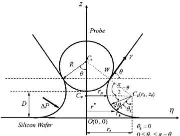
The profile of a water bridge formed between the probe tip and the silicon wafer surface is here determined by the balance of all external forces acting in the column of this water bridge. As Fig. 1 shows, the lateral surface of this wafer bridge is formed by a circular curve with its center located at point CK. This circular curve is tangential to both the circular profile of the probe tip and the flat wafer surface. If W in Fig. 1 denotes the contact point of the circular profile of the probe tip and the lateral surface of this wafer bridge, then the center of the probe tip 共Ct兲 and point W and the center of the lateral surface共CK兲 are connected to form the straight line. In Fig. 1, rK denotes the kelvin radius, R de-notes the radius of the probe tip, r0denotes the radius of the cross section of the water bridge formed on the wafer sur-face, and D denotes the minimum distance between the
probe tip and the wafer surface. If rN denotes the minimum radius formed at the neck of the water bridge, then it satisfies
rN+ rK. = r0.
In this figure, r0and rKare two unknowns which can be determined by the balances of all external forces applied to the water bridge. In the present study, the workpiece共wafer兲 is moving at a very small velocity such that the water bridge can be approximated to be geometrically symmetric with re-spect to the z axis. If the surface tension coefficient of the water bridge is ␥, the surface tension forces are formed around the circle made up of all W points and the circle on the wafer surface with point O as its origin and r0 as its radius. Since the lateral surface of the water bridge is tan-gential to the wafer surface, the surface tension forces formed on the wafer surface are thus canceled out due to their symmetry with respect to the z axis. We define to be the angle between the surface tension ␥ and the horizontal surface. The surface tension force 共F1兲 acting on the water bridge is obtained to be the integration of the␥component in the z direction around the circle made up of all these W points. Therefore, F1 is obtained as
F1= 2R␥sin2. 共1兲
The water bridge is formed to be a saddle type. The pressure difference across its lateral surface共⌬P兲 can be determined by the Young-Laplace equation.34 If the radius of the cross section of the water bridge at an arbitrary z distance from the wafer surface is r*, the pressure difference ⌬P across the lateral surface of water bridge can be expressed as
⌬P =␥
冋
1r*− 1
rk
册
. 共2兲
The force component in the z direction共F2兲 due to the exis-tence of this pressure difference can be expressed as
FIG. 1. Schematic diagram of a water bridge formed between a probe and a silicon wafer.
F2= −
冕
0 − 共2r*rkdk兲⌬P cosk = −冕
0 − 2r*rk␥冉
1 r*− 1 rk冊
coskdk = − 2rk␥冋
冉
1 − r0 rk冊
sin−1 4cos 2+ 1 4册
. 共3兲The z-directional force balance in the water bridge gives
F1+ F2= 2R␥共sin兲2− 2rk␥ ⫻
冋
冉
1 −r0 rk冊
sin−1 4cos 2+ 1 4册
= 0, 共4兲 where= sin−1关r 0/共R+rk兲兴. By the triangle ⌬CtCWCK, r02+共R + D − rk兲2=共R + rk兲2. 共5兲Equations共4兲 and 共5兲 can be coupled to solve r0and rKif the distance D is known. The surface profile of the water bridge can thus be determined.
B. Static electricity field including the effect of space charges
In the oxidational process arising in an atomic force mi-croscopy, the protons which are the hydrogen ions created in the dissolution of water under an electrical voltage are en-trapped in the oxide film as space charges. These space charges give a partial contribution to the total static electric-ity field. For the static electricelectric-ity field generated by applying a Vox voltage in the water bridge without taking the space charges into account, its value between a sphere and a flat plate is expressed as35
E共兲 =1
2
R共R + X兲共R + 2X兲
X关共R + X兲2+2兴3/2Vox, 共6兲
where X denotes the film thickness of the oxide film, Vox represents the electrical voltage formed applied between the probe and the wafer plate, and, as Fig. 1 shows, denotes the distance of a point on the wafer surface far from the origin O. In the present study, the radius of curvature at the probe tip is about 100 nm. This value is much larger than the thickness of the oxide film 共about 1 nm兲. Therefore, R+X ⬵R and R+2X⬵R. Equation 共6兲 can be further simplified as
E共兲 = R 3
2X共R2+2兲3/2Vox. 共7兲
The mechanism of the space charges entrapped in the oxide film must be known before considering the effect of space charges on the static electricity field. We define h as the volume of one space charge and V as the total volume occu-pied by the total space charges accumulated in the oxide film, then h / VⰆ1. The space charges within the oxide film will be moved by applying a high electrical voltage such that they are repelled and accumulated at the thin layer nearby the oxide film surface.
If N is the number of space charges inside of the oxide film, N0共=V/h兲 denotes the number of space charges in the oxide film with a volume of V , z is the ion valence, and q represents the electrical charge of an electron 共q=1.6 ⫻10−19C兲. The ordinary differential equation of N can be solved by applying the initial condition t = 0 and N = 0. The solution was obtained as33
N = N0ln
冉
1 + zqCoxX0
冊
, 共8兲
where0denotes the surface electrical charge density gener-ated by a single space in the oxide film 共unit: C/m2兲 and Cox= 4⫻1022/ cm2for the SiO
2film. Equation共8兲 shows the relation between N and X. In a close contour with an area of
S, the surface integration of the electrical field 共E兲 over this
area 共S兲 is equal to the total electrical charges enclosed by this close contour 共Qenclosed兲 divided by the permittivity of the medium 共兲. Therefore,36
冕
sE · dS =Qenclosed
. 共9兲
Since the top and bottom surfaces of a thin layer have almost the same area S, the integration of Eq.共9兲 can be expressed as
E · 2S =Qenclosed
=
Qox
共10兲
if the electrical field共E兲 is assumed to be uniformly distrib-uted. Therefore, the magnitude of the electrical field induced by the space charges共Qox兲 is E=Qox/ 2S. This induced elec-trical field is in the direction exactly opposite to that of the electrical field 共E兲 due to the application of an electrical voltage between the probe and the wafer surface. The com-bined electrical field共Ec兲 can thus be written as
Ec= E −共Qox/2S兲, 共11兲
where the E value can be obtained by using Eq.共7兲. Qoxcan be obtained to be the product of the electricity of one elec-trical charge 共zq兲 and the number of the electrical charges within the oxide film共N兲. Then,
Qox= zqN. 共12兲
Substituting Eqs. 共7兲, 共8兲, and 共12兲 into Eq. 共11兲 gives the combined electrical field 共Ec兲 as
Ec= R3 2X共R2+2兲3/2Vox− zq 2sln
冉
1 + zqCoxX 0冊
, 共13兲where s = S / N0. An attenuation of the electrical field due to the increase in the oxide film thickness is thus taken into account in Eq.共13兲.
C. Kinematics of oxidational reaction
The Cabrera-Mott theory32 is applied in the present study to detail the growth behavior of the oxide film. The activation energy is employed in this theory to describe the diffusion behavior of ions in the oxide film. Since interstitial defects are formed in the oxide film, the OH− ions diffuse
into the wafer surface through continuous interstitial jumps when the ion energy is sufficiently high to overtake the re-quired activation energy. The possibility of an ion perform-ing interstitial jumps in a unit of time is proportional to exp共−W/kBT兲, where W denotes the activation energy needed
in continuous interstitial jumps共W=0.15 eV兲, kBis the Bolt-zmann constant 共kB= 1.38⫻10−23J / K兲, and T denotes the absolute temperature 共K兲. When an external electrical field 共E兲 is applied, the interstitial jump is lowered by zqa
⬘
E / 2 ifthe jump of a positively charged ion is in the same direction as the electrical field. Then, the activation energy is now modified as W − zqa
⬘
E / 2kBT. Here, a⬘
denotes the average distance between two adjacent interstices 共unit: Å兲. If the jump is opposite to the direction of the electrical field, the activation energy is modified to be共W+zqa⬘
E / 2kBT兲. When the possibilities of these two directions are taken into ac-count in the evaluation of the moving velocity共u兲 of an ion at the inside of the oxide film, the ion velocity can be ex-pressed as32u =␥0a
⬘
冋
exp再
−冋
W −共zqa
⬘
E/2兲 kBT册
冎
⫻− exp再
−冋
W +共zqa⬘
E/2兲kBT
册
冎
册
, 共14兲
where␥0 denotes the average jumping frequency of an ion 共unit: 1/s兲. Since the E value in the oxidational process is considerably large共⬎1 V/nm兲, Eq. 共14兲 can be further ap-proximated as
u⬵␥0a
⬘
exp冉
− WkBT
冊
exp
冉
zqa⬘
E2kBT
冊
, 共15a兲if the ions are positively charged. If the ions are negatively charged, Eq.共15a兲 is slightly modified as
u⬵␥0a
⬘
exp冉
− WkBT
冊
exp
冉
− zqa⬘
E2kBT
冊
. 共15b兲Actually, Eqs.共15a兲 and 共15b兲 show the same magnitude. We define a⬅a
⬘
/ 2 and u0⬅2␥0a exp共−W/kBT兲, then Eq. 共15a兲 can be rewritten as32u⬵ u0exp
冉
zqa⬘
E2kBT
冊
. 共16兲A chemical reaction arising in the AFM oxidation can be divided into two types:共1兲 the reaction limit type and 共2兲 the diffusion limit type. The reaction limit type always appears at the initial stage in which the chemical reaction is predomi-nant. As the oxide film is formed on the substrate, it is rap-idly transformed to the diffusion limit type. Under the con-dition of a high electrical field, it is advantageous to lower the activation energy required for ion diffusions. The Cabrera-Mott theory was developed on the basis that the dif-fusions are predominant in the chemical reaction. In this theory, the oxide film is assumed to be formed so long as the ions can reach the reaction interface by diffusions. With this assumption, the growth rate of the film thickness共dX/dt兲 is considered to be equal to the ion velocity共u兲 in the diffusion process. Then,
u = dX/dt. 共17兲
Then, Eq.共17兲 can be rewritten as
dX
dt = u0exp
冉
zqa⬘
EkBT
冊
. 共18兲
Substitution of Eq.共13兲 into Eq. 共18兲 gives
dX dt = u exp
再
冋
R3 2X共R2+2兲3/2 zqa⬘
kBT Vox − z 2q2a⬘
2kBTsln冉
1 + zqCoxX 0冊
册
冎
. 共19兲 We define zqa⬘
kBT Vox⬅ Xa, 0 zqCox⬅ Xb, z2q2a⬘
2kBTs ⬅␦. Then Eq.共19兲 can be rewritten asdX dt = u exp
再
冋
R3 2X共R2+2兲3/2册
Xa−␦ln冉
1 + X Xb冊
冎
. 共20兲 Equation共20兲 is an ordinary differential equation developed for the film thickness X. It is applicable to solve the film thickness numerically as a function of time when a dc elec-trical voltage is applied in the AFM oxidation process. How-ever, it is valid by assuming no side effect of the electrical charges accumulated in the oxide film on the sequential growths of this oxide film.D. Effect of ac voltage on AFM oxidation
In the AFM oxidation process, the application of an ac electrical voltage is simply for the purpose of getting rid of the space charges entrapped in the oxide film as much as we possibly can. These space charges are generally harmful for the growth rate of the oxide film on the substrate surface. The period of an ac electrical voltage is made up of a posi-tive voltage pulse followed by a negaposi-tive voltage pulse.
However, there generally exists a magnitude difference between these two voltages because of their different pur-pose. The positive voltage pulse is applied to grow the oxide film as this voltage is sufficiently high. The negative voltage pulse is then applied to get rid of the space charges accumu-lated in the oxide film during the oxidational process. How-ever, these space charges are unable to be eliminated com-pletely just by applying a negative voltage, and the degree of removal is still dependent upon the magnitude of the nega-tive voltage pulse. Therefore, the residual space charges can still obstruct the growth of the oxide film formed in the fol-lowing cycles. We define the number of space charges before the removal by applying a negative voltage to be Q0, the number of the removed space charges and the number of space charges residual in the oxide film after the step of elimination to be Q. The residual proportion of space charges 共␣兲 is thus defined as
␣⬅ Q
Q0
= 1 −Q0− Q
⬘
Q0
. 共21兲
Then, Eq.共13兲 for the electrical field developed for dc elec-trical voltage is now slightly modified for ac voltage as
Ec= R3 2X共R2+2兲3/2Vox− zq 2SN0ln
冉
1 +␣ zqCoxX 0冊
. 共22兲 The growth rate of the oxide film thickness is thus expressed as dX dt = u exp再
冋
R3 2X共R2+2兲3/2Xa−␦ln冉
1 +␣ X Xb冊
册
冎
. 共23兲 In Eq.共23兲, the␣value is determined by the method shown in the next section. It is the proportional value obtained from the application of the first negative voltage in order to get rid of the space charges.The oxide film thickness as a function of time can be obtained by applying the numerical method to Eq. 共23兲. It should be mentioned that Eq.共23兲 is also valid for the system with a very small relative velocity between the probe tip and the specimen. The differential equation developed for a non-zero sliding velocity seems very difficult to solve.
E. Determination of the residual proportion of space charges
The residual proportion of the space charge共␣兲 in Eq. 共23兲 can be determined by developing an expression for the electrical charges共Q兲 created in the oxidational process as a function of the static electricity force 共Fe兲. Then, the static electricity force is obtained experimentally by using the Kelvin force microscopy of a SPM.
Coulomb’s law is applied here to evaluate the static elec-tricity force共Fe兲 formed in a sphere with its center a distance
d0from a flat surface. The electrical charges in the probe are mostly accumulated on the spherical surface of the probe tip, since the radius of the probe tip is very small compared to the dimension of a square area on the wafer surface. The static electrical force can thus be developed for a point charge above a flat surface. By Coulomb’s law, the static electricity force Fedue to the electrical charges Q accumu-lated at the probe tip is expressed as
Fe= −
冕
−L/2 L/2冕
−L/2 L/2 vd0XQ 4共x2+ y2+ d02兲3/2dxdy, 共24兲 where L denotes half of the edge length of this square area, and it is always chosen to be a sufficiently large value in the integration or Eq.共24兲,v denotes the space-charge density in the oxide film, is the permittivity of the oxide film 共 = 3.453⫻10−11C2/ J m兲, and d0 represents the distance of the sphere center of the probe tip from the wafer surface. The space-charge densityv共v= Q / XL2兲 in Eq. 共24兲 is replaced by the space charge Q, and Q is assumed to be a constant value. The integration of Eq.共24兲 can be rewritten as
Q =
冑
− L2Fe/冕
−L/2 L/2冕
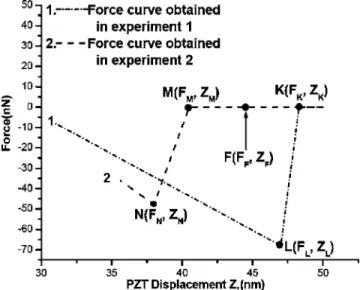
−L/2 L/2 d0 4共x2+ y2+ d02兲3/2dxdy. 共25兲 The Q value in Eq.共21兲 can be obtained from Eq. 共25兲 if the static electricity force Feis available. In order to determineFe, the KFM is then employed to measure the interaction force curve formed between the spherical tip and the wafer surface. Two kinds of force-displacement experiments have been conducted in the present study. The first kind of force-displacement curve was obtained from the wafer surface be-fore growing the oxide film. In this case, the interaction force formed between the tip and the wafer is mainly due to the van der Waals force. The second kind of force-displacement curve was then obtained after growing the oxide film. Since the space charges accumulate in the oxide film, the interac-tion force obtained from this measurement is thus enhanced by the static electricity force. Figure 2 shows the example of these two kinds of force-displacement profiles. Curve 1 indi-cates the profile for the wafer after growing the oxide film, whereas curve 2 indicates the profile before growing the ox-ide film. Theoretically, an intact profile of the Kelvin force measurement includes one force-displacement curve for the advancing motion and the other curve for the receding mo-tion of the probe. However, only the part in the advancing motion is shown in each of these two kinds of experiments in order to evaluate the static electricity force. In Fig. 2, L and
N are the jump-into-contact points of curves 1 and 2,
respec-tively. The PZT displacement corresponding to point L on curve 1 is obviously larger than that of point N on curve 2 because a static electricity force exists in the former. Points
K and M denote the incipient points of curves 1 and 2,
re-spectively, where the jump-into-contact behavior is just right. The forces of points K , L , M, and N are FK, FL, FM, and FN, respectively. We define d to be the distance between the probe tip and the sample surface, it can be determined if the sum of the PZT displacement and the deflection of the can-tilever due to the interaction 共attractive兲 force formed
be-FIG. 2. Schematic diagram of the interaction forces formed under the con-ditions of experiments 1 and 2.
tween the probe and the sample surface is available. In the case of curve 1, the distance between the probe tip and the sample surface, d1, corresponding to point K is expressed as
d1=共ZK− ZL兲 + 共FK− FL兲/kZ, 共26a兲
where共ZK− ZL兲 denotes the PZT displacement, kzdenotes the spring constant of the cantilever, and therefore 共FK− FL兲/kz denotes the cantilever deflection due to the interaction force which comprises the van der Waals force and the static elec-tricity force. In the case of curve 2, the distance between the probe tip and the sample, d2, corresponding to point M is expressed as
d2=共ZM− ZN兲 + 共FM− FN兲/kZ, 共26b兲
where 共ZM− ZN兲 denotes the PZT displacement, and 共FM − FN兲/kzdenotes the cantilever deflection due to the van der Waals force only formed between them. The following method can be done to find the static electricity force共Fe兲 in order to calculate the space charge shown in Eq. 共25兲. We define point F to be one point on the KL line such that the distance of the probe tip from the wafer surface has the same value as d2. Then d2 can be expressed as
d2=共ZF− ZL兲 + 共FF− FL兲/kZ, 共27a兲
where FF denotes the interaction force corresponding to point F. We define the slope for the KL line to be mKC, then Eq.共27a兲 can be rewritten as
d2=共ZF− ZL兲 + mKL共ZF− ZL兲/kZ
=共ZF− ZL兲共1 + mKL/kZ兲. 共27b兲
Equation 共27b兲 can be used to determine ZF because the other parameters in Eq.共27b兲 are obtained from the measure-ments. This ZF value is then substituted into Eq. 共27a兲 to obtain FF. Since FFdenotes the van der Waals force created at point F, the static electricity force Feis then obtained as
Fe=兩FF− FK兩 = 兩FF− FM兩. 共28兲
Curve 1 represents the force-displacement profile obtained from the measurement of a specimen after applying only the positive portion of an ac voltage, whereas curve 2 represents the profile obtained from the measurement of the same speci-men after the removal of the space charges by applying a negative voltage. Then, the Q value obtained from Eq.共25兲 denotes the space charges which have been removed due to the use of the negative voltage pulse.
III. EXPERIMENTAL DETAILS
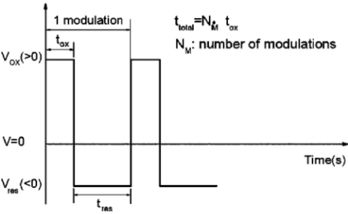
All the oxidational experiments were carried out on a scanning probe microscope共SPM, Solver SNOM model, NT-MDT兲 by using the function of electrical chemical AFM. In the ac system, the voltage applied to the system was present in a cyclic form, as shown in Fig. 3. Each cycle共one modu-lation兲 comprises of a positive voltage pulse, Vox, followed by a negative voltage pulse, Vres. The positive voltage pulse is simply employed to produce the oxide film on the speci-men surface, whereas the negative voltage pulse is applied to reduce or remove the space charges accumulated in the oxide film. The durations for the positive and negative voltages are
tox and tres, respectively. These two durations in the present study are freely given and controlled by a computer. The magnitudes of Voxand Vrescan be varied in a range of 0–10 V. In a modulation, the acting time for Voxis tox共s兲, and the acting time for Vresis tres. The time ttotalparameter is defined as the product of tox and the modulation number. The space charges accumulated in the oxide film and its surface voltage were measured on a scanning probe microscope共SPM, SPA 300HV, Seiko兲 by using its two modes. The AFM contact mode was applied to measure the force-displacement profiles which were produced before and after applying a negative voltage pulse, respectively. The KFM mode was applied to detect the variations of the surface potential of an oxide film after applying different times of negative voltage pulses to determine the residual proportion␣of space charges at each times. The probe used in the present study uses silicon as the substrate and gold as the coating film. The spring constant of the cantilever共K兲 is 3 N/m, the natural frequency 共f0兲 of the probe is 29 kHz, and the radius of curvature at the probe tip 共R兲 is 100 nm.
The substrate material of the specimen is made of the
n-type wafer with 关100兴 as the crystal orientation and the
resistivity is in a range of 1–100⍀. The wafer substrate was rinsed with de-ionized共DI兲 water, 10 wt % HF, and acetone in sequence before the application of either the electric chemical atomic force microscopy 共EC AFM mode兲 or the Kelvin force microscopy共KFM mode兲. Two kinds of experi-ments were carried out. The first kind of experiexperi-ments was carried out to produce an oxide film in a square area of 3 ⫻3m2 by applying 10 V to the system 共SPM, Solver SNOM model兲 and scanning at a sliding velocity of 1500 nm/ s. Then the specimen was moved to the KFM mode of a scanning probe microscope 共SPA 300HV, Seiko兲 to achieve the synchronous measurements of surface electri-cal potential and morphology. After this, the AFM mode was applied to remove the space charges that accumulated in the oxide film of the same area by applying a negative voltage pulse 共−4 or −6 V兲 as well as at a scanning velocity of 0.75m / s. The AFM mode was able to attain the force-displacement curves for the specimens before and after re-moving the space charges by applying a negative voltage pulse. The second kind of experiments was prepared by us-ing the AFM mode. The oxide films were produced by givus-ing either an ac or dc voltage in the system, but no scanning
velocity was applied to the specimen during the growth of the oxide film. The specimens prepared by this kind of ex-periments were simply used for the measurements of the film thickness and the morphology formed at a point. The results of these measurements were compared to the results pre-dicted by the solution of Eq.共23兲 to check the validity of the present model.
IV. RESULTS AND DISCUSSION
The theoretical solutions of rN 共the radius of the water bridge at the neck兲 and r0 共the radius of the water bridge formed on the wafer surface兲 shown in Fig. 1 are varied with the minimum distance between the probe tip and the wafer surface共D兲 and the radius of curvature of the probe tip 共R兲. They are shown in Table I for two different probes with R = 100 nm and R = 150 nm, respectively. The value of either
rNor r0was found to be strongly dependent upon the radius of curvature at the probe tip共R兲 but only slightly dependent upon the distance D. Both rNand r0present a linear relation-ship with R. In the present study, the oxide film was gener-ated by the EC AFM using the contact mode. The repulsive force that formed between the probe tip and the wafer sur-face allows an extremely small gap existing between them. This minimum gap 共D兲 is usually very difficult to obtain effectively. The commonly used value of D is 0.54 nm which is estimated to be equal to the sum of the radii of two adja-cent atoms.37According to the theoretical results shown in Table II, the effect due to the change in the minimum gap 共D兲 in a range of 1–5 nm on the r0and rkvalues is evaluated to be insignificant, irrespective of the radius of the probe tip. That is, an arbitrarily given value for D in this range does not
affect the profile of the water bridge significantly since the oxide film thickness 共X兲 can be obtained directly from the measurements of AFM and it is always varied in the range of several nanometers. The oxide film thickness 共X兲 in the present study is thus taken as the approximate value of the minimum gap共D兲 in the following evaluations of the oxide film parameters. These parameters are then compared to the experimental results in order to verify the trustworthiness of the theories developed in this study.
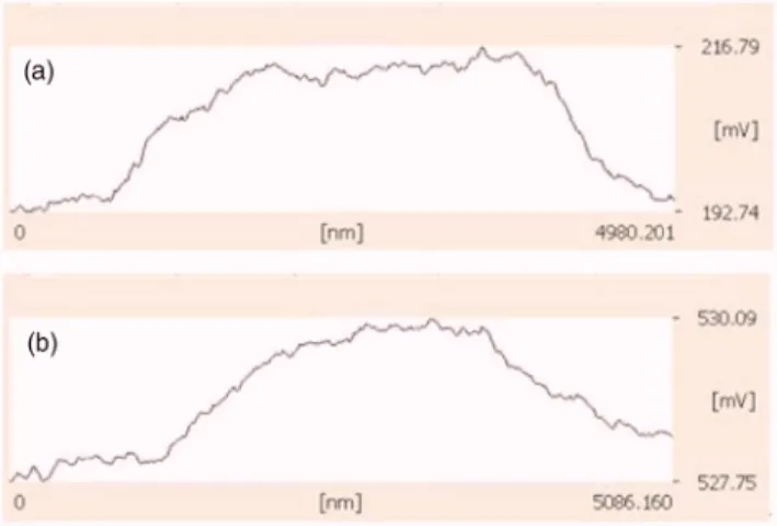
The EC AFM function of a scanning probe microscope was applied to produce an oxide film in a 3⫻3m2square area. Then the Kelvin force microscopy was employed to measure the electrical potentials of this square area. The electrical potential which was obtained for the specimen be-fore applying a negative voltage pulse to remove the space charges is shown in Fig. 4共a兲, while the potential obtained for the specimen after applying a voltage of −4 V is shown in Fig. 4共b兲. The profile of Fig. 4共a兲 shows the measure of the electrical potential in the plateau region to be about 18 mV, while the electrical potential for the specimen after applying two negative voltage pulses is lowered to 1.8 mV. This elec-trical potential was found to be barely changed if the nega-tive voltage was applied more than twice. The removal per-formance of the space charges in the oxide film is dependent upon two influential factors; one factor is the magnitude of the applied negative voltage pulse and another is the number of modulations applied to remove the space charges. The magnitude of electrical potential can be expressed in terms of the tip-specimen distance exactly at the instant of jump into
TABLE I. Theoretical results for the geometric dimensions of the water bridges formed by two radii of probe tips.
R共nm兲 D共nm兲 rn共nm兲 rk共nm兲 r0共nm兲 1 109.2 46.0 155.2 2 108.4 46.3 154.7 100 3 107.9 46.3 154.2 4 107.2 46.8 154.0 5 106.5 46.2 152.7 1 162.7 73.2 235.9 2 162.3 73.0 235.3 150 3 161.9 72.9 234.8 4 161.4 72.7 234.1 5 160.9 72.6 233.5
TABLE II. Experimental results of the static electricity force and the evaluations of the residual proportions of space charges corresponding to two negative voltages.
Parameters
Negative voltage共V兲 Number of scannings d0共nm兲 Fe共nN兲 Q0共⫻10−15C兲 Q0− Q⬘共⫻10−15C兲 ␣
4 1 8.9 44.09 4.17 2.35 0.44
2 6.8 20.75 1.82 1.82 0
6 1 7.5 47.72 4.45 3.2 0.28
2 6.9 9.86 1.25 1.25 0
FIG. 4. 共Color online兲 Electrical potentials 共a兲 before applying a negative voltage pulse and共b兲 after applying a negative voltage pulse 共Vres= −4 V兲 as well as scanning twice. The oxidational voltage共Vox兲 is 10 V.
contact. The magnitude of electrical potential is proportional to this distance. In order to investigate the removal effect of space charges by applying a negative electrical voltage pulse, the electrical potential of a native oxide film on a wafer was measured as the reference potential. The native oxide film was prepared by exposing a wafer in the atmosphere for a period of time. The space charges accumulated in this native oxide film were also measured and expressed by the specimen distance. The experimental results of the tip-sample distance for two kinds of negative voltage pulses as well as three kinds of modulation numbers are shown in Fig. 5. The measure of the distance for the native oxide film is about 7 nm. The application of the first negative voltage pulse is indeed helpful to remove the space charges in the oxide film; however, the removal rate of space charges is significantly attenuated further by increasing the number of times a negative voltage pulse is applied. As Fig. 5 shows, the difference between the first and the second times is quite small. It can also be investigated that the magnitude of the tip-sample distance after two times of scannings drops to the level almost the same as the native oxide film. This result implies that the accumulated space charges formed in the process of EC AFM can be largely removed by applying two negative voltages pulses, irrespective of the magnitude of the negative voltage applied to the system. The influence of the negative voltage magnitude on the tip-sample distance is relatively small compared to the influence of the modulation number. Nevertheless, the removal effect of the space charges is slightly enhanced by increasing the magnitude of the negative voltage pulse.
The tip-specimen distances 共d2 or d0兲 shown in Fig. 5 can be used to evaluate the residual fraction共␣兲 of the space charges after scanning the surface by a negative voltage pulse共Vres兲. The maximum scanning number for the removal of space charges is 2 in the present study. Table II shows the data of␣ obtained from the KFM and AFM experiments by differing the Vresvalue共−4 and −6 V兲 as well as the scanning number. The results show that the residual fraction 共␣兲 is lowered to a value much smaller than 1 / 2 even by one scan-ning. The ␣ value drops to be almost zero as the second
scanning is applied; its value corresponding to the first scan-ning is effectively lowered by elevating the magnitude of
Vres. The theoretical heights of the oxide film varying with the oxidational time can be predicted by the present model as a function of the positive voltage applied to the system. Fig-ure 6 shows the theoretical results of the oxide height pro-duced by applying −4 V to remove the space charges as well as five kinds of positive voltages 共Vox兲 to grow the oxide film. These curves show the behavior that the height of oxide film is grown proportionally to the oxidational time. How-ever, the growth rate which can be determined by the slope of a curve is decreased by increasing the time. For a fixed oxidational time, the height of oxide film is increased by elevating Vox if Vox is high enough to start the oxidational reaction.
The validity of the theoretical model developed in the present study can be confirmed by the experiments carried out at different combinations of Vox and Vres. Figure 7共a兲 shows both the experimental and theoretical results obtained from Vox= 10 V as well as two kinds of Vresvalues共−6 and −4 V兲, whereas Fig. 7共b兲 shows the results obtained from the
Voxvalue lowered to 8 V. The trend exhibited in the experi-mental results of the oxide height due to the change in the oxidation time is consistent with that predicted by the theo-retical results, irrespective of the Vox value applied to the system. However, the behavior exhibited in the experimental results due to the change in the Vres value is considerably different from the behavior of the theoretical results pre-dicted by the present model. As for the experimental results, the oxide height formed at a fixed oxidational time by Vres = −6 V is unexpectedly smaller than that by Vres= −4 V. This behavior is obviously contrary to the theoretical predictions. In either Fig. 7共a兲 or Fig. 7共b兲, the experimental results cor-responding to Vres= −4 V show a good fit with the theoretical results expressed by a dashed curve. However, the experi-mental results obtained by applying Vres= −6 V are lower than the theoretical results, with different errors. This un-usual behavior, also presented in the study of Pérez-Murano
et al.,17was explained to be related to the oxidation arising at
FIG. 5. The interdistance between probe tip and the sample obtained right at the jump into contact. They are evaluated at two Vresvalues as well as
different times of Vresto remove space charges. FIG. 6. The theoretical results of the oxide height varying with time and
the tip of the probe. In the case of兩Vres兩⬍−6 V, no oxidation was formed at the probe tip. Their experimental results indi-cate that the oxide height is indeed increased by increasing the magnitude of Vres 共with a negative value兲 because the removal of the space charges from the oxide film can be enhanced. As to the results in the case of 兩Vres兩⭌−6 V, the removal of space charges was somewhat impeded by the occurrence of the oxidation at the tip of the probe. This oxi-dation behavior causes the experimental results correspond-ing to Vres= −6 V to be conversely lower than that when applying Vres= −4 V. The function of Vox as to the oxide height can be evaluated on the basis of the same oxidational time. The experimental results indicate that the oxide height is generally increased by elevating Vox. However, the differ-ence in the increasing rate of oxide height resulting from the difference in Vox is gradually narrowed to a small value as the oxidational time becomes sufficiently long. We define 共t兲total to be the product of the oxidational time tox and the modulation number. For a fixed value of 共t兲total in the EC AFM, the modulation number can be altered by adjusting the time periods of the positive and negative voltage pulses in a modulation. Experimental results of the oxide height shown
in Fig. 8 were obtained by fixing the time共t兲totalto be 3 s but differing the modulation number. The results labeled as “dc oxidation” mean that no negative voltage pulses were ap-plied and the modulation number is thus equal to 1. The experimental results show that the oxide height obtained from the application of the dc voltage is the smallest of these three kinds of modulations. The increase in the modulation number in a fixed time period is helpful to increase the oxide height, irrespective of the oxidational voltage Vox. This figure also provides evidence that the removal of the space charges by applying a negative voltage pulse as well as the increase in the modulation frequency advantageous to the increase in the oxide height.
Apart from Vox, Vres, and tox, the time period of having a negative voltage pulse in a modulation共tres兲 is also an influ-ential factor to the growth of the oxide film. That is, the time period tres in a modulation becomes of importance to the quantity of the space charges removed from the oxide film. Figures 9共a兲 and 9共b兲 show the heights of the oxide films produced by two different tres values, they are obtained by applying Vox= 10 V and Vox= 8 V, respectively. In these two figures, the negative voltage was set to be −4 V and toxto be 0.1 s. The curves in these two figures represent the theoreti-cal results predicted by the present model. The good fit be-tween the theoretical and experimental results indicates that the present model is trustworthy. Both Figs. 9共a兲 and 9共b兲 show the elongation of tres to be advantageous in increasing the thickness of oxide film. The difference in the oxide film due to different applications of tresis enhanced by either the elevation of the oxidational voltage共Vox兲 or the elongation of the total oxidational time.
V. CONCLUSIONS
From the theoretical analyses for the profile of the water bridge, either the value of rnor r0is strongly dependent upon the radius of the probe tip but only slightly dependent upon the minimum distance between the probe tip and the wafer surface共D兲.
FIG. 7. The theoretical and experimental results of the oxide height gener-ated by共a兲 Vox= 10 V and共b兲 Vox= 8 V. The theoretical results evaluated by
both ac and dc oxidations are presented to compare.
FIG. 8. Oxide heights created by the dc and ac oxidations and at two different Voxvalues. The total oxidation time is 3 s.
The removal performance of the space charges accumu-lated in the oxide film is influenced by the magnitude of the negative pulses of an ac voltage and the number of negative voltage modulations applied to remove the space charges. The removal rate is significantly lowered by increasing the number of times of negative voltage pulses. The accumulated space charges can be largely removed by two negative volt-age pulses, irrespective of the magnitude of the negative voltage pulse applied to the system. The influence of the negative voltage magnitude on the removal of space charges is quite small.
The residual fraction of the space charges 共␣兲 corre-sponding to the first scanning is effectively lowered by el-evating the magnitude of Vres.
The behavior exhibited in the experimental results of oxide height due to the change in the oxidation time is con-sistent with that predicted by the theoretical results, irrespec-tive of the Voxvalue applied to the system. The experimental
results due to the change in the Vres value match well the theoretical results if Vres= −4 V is applied; however, the dif-ference between these two results becomes significant as Vres value is elevated to −6 V due to the oxidation of the probe tip.
The height of the oxide film is generally increased by elevating Voxwhich is applied to grow it. However, the dif-ference in the increasing rate of oxide height resulting from the application of different Vox is generally narrowed to a quite small value as the oxidational time becomes suffi-ciently long.
The increase in the modulation number 共or frequency兲 within a fixed time period is helpful to increase the oxide height, irrespective of the voltage value of Vox. The elonga-tion of tresis advantageous to increase the thickness of oxide film if the parameters of Vres, Vox, and tox are fixed in the oxidational process.
1J. A. Dagata, J. Scneir, H. H. Harary, C. J. Evans, M. T. Postek, and J.
Bennett, Appl. Phys. Lett. 56, 2001共1990兲.
2L. A. Nagahara, T. Thundat, and S. M. Lindsay, Appl. Phys. Lett. 57, 27
共1990兲.
3J. A. Dagata, J. Schneir, H. H. Harary, J. Bennett, and W. Tseng, J. Vac.
Sci. Technol. B 9, 1384共1991兲.
4S. T. Yau, X. Zheng, and M. H. Nayfeh, Appl. Phys. Lett. 59, 2457
共1991兲.
5N. Bamiol, F. Pérez-Murano, and X. Aymerich, Appl. Phys. Lett. 61, 462
共1992兲.
6H. Sugimura, N. Kitamura, and H. Masuhara, Jpn. J. Appl. Phys., Part 1 33, L143共1994兲.
7P. Fay, R. T. Brokenbrough, G. Abeln, P. Scott, S. Agarwala, I. Adesida,
and J. W. Lyding, J. Appl. Phys. 75, 7545共1994兲.
8H. Sugimura, T. Yamamoto, and N. Nakagiri, Appl. Phys. Lett. 65, 1569
共1994兲.
9N. Kramer, J. Jorritsma, H. Birk, and C. Schönenberger, J. Vac. Sci.
Tech-nol. B 13, 805共1995兲.
10H. C. Day and D. R. Allee, Appl. Phys. Lett. 62, 2691共1993兲. 11M. Yasutake, Y. Y. Ejiri, and T. Hattori, Jpn. J. Appl. Phys., Part 1 32,
L1021共1993兲.
12T. Hattori, Y. Ejiri, and K. Saito, J. Vac. Sci. Technol. A 12, 2586共1994兲. 13E. S. Snow and P. M. Campbell, Appl. Phys. Lett. 64, 1932共1994兲. 14T. Teuschler, K. Mahr, S. Miyazaki, M. Hundhausen, and L. Ley, Appl.
Phys. Lett. 66, 2499共1995兲.
15T. Teuschler, K. Mahr, S. Miyazaki, M. Hundhausen, and L. Ley, Appl.
Phys. Lett. 67, 3144共1995兲.
16A. E. Gordon, R. T. Fayfield, D. D. Litfin, and T. K. Higman, J. Vac. Sci.
Technol. B 13, 2805共1995兲.
17F. Pérez-Murano, G. Abadal, N. Barniol, X. Aymerich, J. Servat, P.
Gor-ostiza, and F. Sanz, J. Appl. Phys. 78, 6797共1995兲.
18J. Servat, P. Gorostiza, F. Sanz, F. Pérez-Murano, N. Barniol, G. Abadal,
and X. Aymerich, J. Vac. Sci. Technol. A 14, 1共1996兲.
19R. Garćia, M. Calleja, and F. Pérez-Murano, Appl. Phys. Lett. 72, 2295
共1998兲.
20R. Garćia, M. Calleja, and H. Rohrer, J. Appl. Phys. 86, 1898共1999兲. 21H. C. Day and D. R. Allee, Appl. Phys. Lett. 62, 2691共1993兲. 22M. Yasutake, Y. Ejiri, and T. Hattori, Jpn. J. Appl. Phys., Part 2 32, L1021
共1993兲.
23D. Stiévenard, P. A. Fontaine, and E. Dubois, Appl. Phys. Lett. 70, 3272
共1997兲.
24J. A. Dagata, T. Inoue, J. Itoh, K. Matsumoto, and H. Yokoyama, J. Appl.
Phys. 84, 6891共1998兲.
25P. Avouris, T. Hertel, and R. Martel, Appl. Phys. Lett. 71, 285共1997兲. 26L. Ley, T. Teuschler, K. Mahr, S. Miyazaki, and M. Hundhausen, J. Vac.
Sci. Technol. B 14, 2845共1996兲.
27P. A. Fontaine, E. Dubois, and D. Stievenard, J. Appl. Phys. 84, 1776
共1998兲.
28F. Pérez-Murano, K. Birkelund, G. Abadal, K. Morimoto, and J. Dagata,
Appl. Phys. Lett. 75, 199共1999兲.
29M. Calleja, J. Anguita, R. Garcia, K. Birkelund, F. Pérez-Murano, and J.
Dagata, Nanotechnology 1, 10共1999兲. FIG. 9. The theoretical and experimental results of the oxide heights
gen-erated by共a兲 Vox= 10 V and共b兲 Vox= 8 V. They are presented to investigate
30M. Calleja and R. Garćia, Appl. Phys. Lett. 76, 3427共2000兲.
31H. Sugimura, T. Uchida, N. Kitamura, and H. Masuhara, J. Chem. Soc. A
98, 4352共1994兲.
32N. Cabrera and N. F. Mott, Rep. Prog. Phys. 12, 163共1949兲. 33E. Dubois and J. L. Bubendorff, J. Appl. Phys. 87, 8148共2000兲. 34W. Adamson, Physical Chemistry of Surfaces, 5th ed.共Wiley, New York,
1990兲.
35R. Garćia, J. Montserrat, and F. Pérez-Murano, Appl. Phys. Lett. 72, 2295
共1998兲.
36D. J. Griffiths, Introduction to Electrodynamics, 3rd ed. 共Prentice-Hall,
Englewood Cliffs, NJ, 1999兲.
37J. N. Israelachvili, Intermolecular and Surface Forces, 2nd ed.共Academic