Strain effect and channel length dependence of bias temperature instability
on complementary metal-oxide-semiconductor field effect transistors
with high-k / SiO
2gate stacks
J. C. Liao,1Y. K. Fang,1,a兲 Y. T. Hou,2C. L. Hung,2P. F. Hsu,2K. C. Lin,2K. T. Huang,2 T. L. Lee,2and M. S. Liang2
1
VLSI Technology Laboratory, Institute of Microelectronics, Department of Electrical Engineering, National Cheng Kung University, Tainan 701, Taiwan
2
Taiwan Semiconductor Manufacturing Company, Hsinchu Science Park, Hsinchu 300, Taiwan
共Received 23 January 2008; accepted 14 July 2008; published online 2 September 2008兲
The strain effect and channel length dependence of bias temperature instability on dual metal gate complementary metal-oxide-semiconductor field enhanced transistors with HfSiON dielectric were studied in detail. For channel length larger than 0.1 m, both positive and negative bias temperature instabilities 共PBTI and NBTI兲 were not affected by the tensile strain obviously. As the channel scaling down to less than 0.1 m, the degradation after PBTI stress was still not influenced by the strain, however, the NBTI degradation was enhanced significantly. In addition, the dependence of BTI on channel length was extensively investigated under constant voltage and field stress. © 2008 American Institute of Physics. 关DOI:10.1063/1.2967442兴
Recently, strained silicon channel and Hf-based high-k/metal gate stack complementary metal-oxide-semiconductor field enhanced transistors共CMOSFETs兲 have been studied extensively for advanced deep-submicron tech-nology applications.1,2 However, the strain engineering is also found to remarkably affect the negative bias temperature instability 共NBTI兲 on conventional polycrystalline silicon/ SiON gate p-type metal-oxide-semiconductor field enhanced transistors共pMOSFETs兲, and this effect is even more signifi-cant for the short channel devices.1,3 On the other hand, the large quantity of bulk traps existing in Hf-based high-k di-electrics cause a critical reliability issue of positive bias tem-perature instability 共PBTI兲 on n-type metal-oxide-semiconductor field enhanced transistors共nMOSFETs兲.4,5So far, the effects of a strained Si channel and its length varia-tion on NBTI and PBTI of Hf-based high-k/metal gate device have not been investigated deeply.
In this work, the strain effects from a tensile SiN capping layer, as well as the channel length dependence, on both NBTI and PBTI of the high-k gate stack devices are studied in detail. It is found that the tensile strain does not affect PBTI or NBTI degradations obviously for channel length larger than 0.1 m. However, as the channel is scaled down to less than 0.1 m, the tensile strain enhances NBTI sig-nificantly, while it still has no influence on PBTI. The mechanism of the channel length dependence is analyzed with the carrier separation experiments.
Devices with high-k/SiO2 gate stacks used in this study were prepared with a foundry’s typical 65 nm CMOS pro-cess. High-k dielectrics 共HfSiON兲 and metal gate were de-posited by atomic layer deposition and physical vapor depo-sition techniques, respectively. Before depositing high-k film, a 9 Å chemical SiO2was used as an interfacial layer共IL兲 to
reduce the interface states. Source/drain implant was acti-vated by a rapid thermal annealing共RTA兲 under 1000 °C for 5 s. HfSiO with Hf/共Hf+Si兲 ratio of 50% was nitrated by
NH3 annealing. The physical thickness of HfSiON
deter-mined from the transmission electron microscopy images was 30 Å. For the investigation of strain effect, a tensile SiN capping layer was deposited to modulate the channel stress as reported previously.6 BTI measurements were performed under stress conditions of 125 ° C, 500 s, and +/−2.5 V gate bias for PBTI and NBTI, respectively.
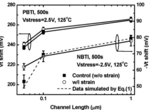
Figure 1 shows the ⌬Vt under constant voltage stress 共CVS兲 of PBTI on nMOSFET and NBTI on pMOSFET with and without the tensile strain as a function of channel length, respectively. From Fig.1, tensile strain does not affect PBTI or NBTI degradations obviously with channel length larger than 0.1 m. However, as the channel scaling down to less than 0.1m, the tensile strain magnifies the NBTI tion profoundly but still has no influence on PBTI degrada-tion. Figure2shows transconductance共Gm兲 loss after NBTI and PBTI stresses. The results of Gm loss reveal that the strain effect also enhances the Gmloss of NBTI for channel length less than 0.1 m, but it has no effect on the Gmloss of PBTI for all channel lengths. It is known that under NBTI stress, the bulk traps can catch the holes or H+ 共positive charged interstitial hydrogen ion兲 released from the broken hydrogen terminated silicon 共Si–H兲 bonds,7 and
conse-a兲Electronic mail: [email protected].
FIG. 1. Both simulated共dash lines兲 and measured 共solid circle and square兲 threshold voltage shifts of the 65 nm HfSiON/SiO2dual metal gate CMOS-FET with and without a tensile strain under NBTI and PBTI stresses as a function of channel length.
APPLIED PHYSICS LETTERS 93, 092101共2008兲
0003-6951/2008/93共9兲/092101/3/$23.00 93, 092101-1 © 2008 American Institute of Physics
quently results in a negative ⌬Vt. Besides, these broken bonds also act as the interface traps共Dit兲 to degrade the Gm. On the other hand, the positive⌬Vtinduced by PBTI stress is mainly related to the electron trapping into high-k bulk traps,5 and thus does not affect the Gmloss. Both the larger −⌬Vtand Gmloss after NBTI stress for a short channel de-vice with a mechanical strain indicate that the tensile strain can break hydrogenated trivalent silicon bonds 共Si3⬅Si − H兲 and thus leads to a larger number of Dit.
In addition, the channel length dependences are observed on both NBTI and PBTI degradations. The absolute value of ⌬Vtdecreases with decreasing channel length for both PBTI and NBTI. To investigate the channel length dependence of NBTI and PBTI, inversion oxide thickness 共Tox,inv兲 was ex-tracted from the measured C-V characteristics for various channel length devices. As shown in the inset of Fig. 3, the Tox,invincreases with decreasing channel length. It has been
reported that the IL regrowth takes place from the oxygen dissolved in the gate stack after high temperature RTA treatment8 and consequently induces higher Tox,inv in short
channel devices. The thicker IL in shorter channel devices suppresses the carriers tunneling and/or results in less elec-tric field stress under CVS to cause less generation of Ditand thus⌬Vtafter NBTI stress. On the other hand, the improved
PBTI characteristics in short channel nMOSFETs are related to the less electron tunneling induced by the thicker IL.
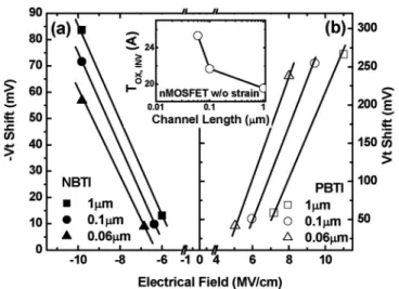
Based on the above observation, IL regrowth is found to strongly affect the channel length dependence under CVS. Hence, the channel length dependence is further investigated with constant field stress 共CFS兲 to prevent the influences of Vtand Tox,inv, as shown in Figs.3共a兲and3共b兲for NBTI and
PBTI, respectively. As can be seen, the short channel pMOS-FETs still show higher ability against NBTI stress, which is similar to that under CVS共Fig.1兲. The same trend in channel length dependence under CFS is attributed to the threshold voltage shift compensation caused by the IL regrowth.
To clarify the channel length dependence of NBTI, car-rier separation measurements are performed under constant electric field. In carrier separation measurement, the gate ter-minal is swept from 0 to −2.5 V with other terter-minals grounded. The measured gate leakage current IGconsists of the substrate current Isub and the IS/D current, respectively. Figure 4 shows the Isub/IG ratio extracted from the carrier separation measurements as a function of channel length un-der a constant electric field for pMOSFET to simulate the CFS of NBTI.The slight increase in the ratio is suspected due to the IL regrowth after high temperature RTA treatment. The thicker IL after regrowth in short channel device suppresses the tunneling of both hole and electron to reduce the IG. Besides, IS/D共hole current兲 is reduced by IL regrowth more profoundly than that of the Isub 共electron current兲 for the
higher barrier height of hole in SiO2. Consequently, the Isub/IG ratio of short channel device is higher than that of long channel devices. The higher fraction of Isub current
leads to the larger quantity of electrons injecting into the high-k dielectric and compensates the NBTI-induced hole trapping. Thus, lower threshold voltage shift in short channel device under NBTI CFS occurs. At the condition of CVS, IL regrowth also compensates the threshold voltage shift and further decrease the stress electric field.
The compensated threshold voltage shift can be modeled as ⌬Vt=⌬VtD it+⌬Vt hole−⌬Vt electronand the threshold volt-age shift due to the trapped electron can be written as ⌬Vt electron=共qNT/Cox·␣兲ln共t/t0兲,
9
where NTis the trap den-sity, t0 is the time constant, t is the stress time, and␣is the fitting parameter correlated with the transport probability of
FIG. 2. Gmlosses of pMOSFET under NBTI stress and nMOSFET under
PBTI stress with and without a tensile strain as a function of channel length.
FIG. 3. The threshold voltage shifts of the HfSiON/SiO2dual metal gate CMOSFET with different channel lengths 共square for 1 m, circle for 0.1 m, and triangle for 60 nm兲 under NBTI 共left兲 and PBTI 共right兲 stresses as a function of electric stress field. The inset represents the Tox,inv of HfSiON/SiO2gate stack as a function of channel length. Two stress voltages 共⫾1.75 and ⫾2.5 V兲 are adopted to extrapolate the relation between electric stress field and threshold voltage shifts.
FIG. 4. The ratio of substrate current density共Isub兲 to gate current density 共IG兲 as a function of channel length under constant electric field for
pMOS-FET. The inset is the schematic band diagram of high-k nMOSFETs with thick 共dash兲 and thin 共solid兲 ILs under constant field NBTI stress, respectively.
092101-2 Liao et al. Appl. Phys. Lett. 93, 092101共2008兲
carriers. The time constant is a function of the capture cross section0and the tunneling current density JG. Considering a uniform distribution of traps, t0 can be derived as t0
= q/JG0.9 Therefore, the compensated threshold voltage
shift can be expressed as ⌬Vt=⌬VtD it+ qNT Cox·␣ ln
冉
t · Jholehole q冊
− qNT Cox·␣ln冉
t · Jelectronelectron q冊
=⌬VtD it + qNT Cox·␣ ln冉
Jholehole Jelectronelectron冊
. 共1兲Here, the interface states density is assumed to be inde-pendent of channel length and ⌬Vt due to NBTI-generated interface states 共⌬VtD it兲 is thus similar for different channel lengths. For simplicity, the hole and electron capture cross sections are assumed to be approximately equal. The ⌬Vt is simulated based on Eq. 共1兲and fits the experimental results, as shown in Fig. 1. With NT= 1.2⫻1010 cm−2 and ␣= 6 ⫻10−3, the fitting is very well, thus evidences that the
thresh-old voltage shift compensation induced by the IL regrowth dominates the channel length dependence. Besides, it is also reported that the density of interface states decreases with increasing the physical thickness of IL.10The improved IL/Si interface quality after IL regrowth may be another possible reason of the better NBTI in short channel device.
For PBTI under CVS stress, the channel length depen-dence can also be explained by the IL regrowth. Short chan-nel device with thicker IL thickness suffers smaller electric field stress. The lower stress field results in less electron trapping and better PBTI. However, under CFS, it is interest-ing that the channel length dependence becomes contradic-tive with that of CVS. We attribute it to the increased trapped charge and less effective detrapping. PBTI is mainly attrib-uted to the electron trapping into pre-existing high-k bulk traps. The density of charging bulk traps Ntrap 共cm−2eV−1兲
under PBTI stress can be expressed as Ntrap
=兰0Xtrap共x,ET兲dx,11 wheretrap 共cm−3eV−1兲 is the bulk trap
volume density, x is the electron tunneling distance, and the ETis the energy depth of bulk trap from the high-k conduc-tion band. The ET at SiO2/high-k interface can be
approxi-mately obtained as ET=⌽SiO2− EOTIL·IL, where⌽SiO2is the
conduction band offset of IL, EOTILis the equivalent oxide
thickness of IL, andILis the electric field in IL. The inset of
Fig.4 shows the schematic band diagram of high-k nMOS-FETs with thick共dash兲 and thin 共solid兲 ILs, respectively. Ac-cording to the expression of ETand the band diagram, the ET at SiO2/high-k decreases with decreased IL thickness
共EOTIL兲. Hence, the short channel device with thicker IL has
larger quantities of filled traps below the Fermi level and suffers severer degradation under PBTI CFS. On the other hand, trapped electrons can be detrapped12via the back tun-neling to channel13even under positive bias. In addition, our
previous study14 found that thicker IL has less detrapping efficiency. Hence, short channel device with thicker IL shows less detrapping efficiency and consequently induces higher degradation under PBTI CFS.
In summary, both the NBTI and PBTI with the channel larger than 0.1 m are not remarkably affected by the ten-sile strain. However, the NBTI are obviously enhanced as the channel length scaling down to less than 0.1 m. On the other hand, the NBTI degradations decrease with decreasing channel length under both CVS and CFS. For the PBTI the channel length dependence is same as that of NBTI under CVS, but is reverse under CFS. Based on the measurements of Tox,invand the carrier separation experiments, the channel
length dependences are attributed to the IL regrowth after RTA treatment. The new observations are helpful to realize the reliability of advanced CMOS devices with high-k gate stack.
This work was supported by the National Science Coun-cil of Taiwan under Contract No. NSC96-2221-E-006-284-MY3, and the authors would like to thank the staff members of TSMC R&D for their helpful support.
1H. S. Rhee, H. Lee, T. Ueno, D. S. Shin, S. H. Lee, Y. Kim, A. Samoilov, P. O. Hansson, M. Kim, H. S. Kim, and N. I. Lee, Tech. Dig. - Int. Electron Devices Meet. 2005, 709.
2K. Ichinose, T. Saito, Y. Yanagida, Y. Nonaka, K. Torii, H. Sato, N. Saito, S. Wada, K. Mori, and S. Mitani, Tech. Dig. VLSI Symp. 2001, 103. 3J. R. Shih, J. J. Wang, K. Wu, Y. Peng, and J. Yue, IEEE Trans. Device
Mater. Reliab., 612共2003兲.
4D. K. Schroder and J. A. Babcock,J. Appl. Phys. 94, 1共2003兲. 5N. Sa, J. F. Kang, H. Yang, X. Y. Liu, Y. D. He, R. Q. Han, C. Ren, H. Y.
Yu, D. S. H. Chan, and D. L. Kwong,IEEE Electron Device Lett.26, 610 共2005兲.
6C. H. Chen, T. L. Lee, T. H. Hou, C. L. Chen, C. C. Chen, J. W. Hsu, K. L. Cheng, Y. H. Chiu, H. J. TaO, Y. Jin, C. H. Diaz, S. C. Chen, and M. S. Liang, Tech. Dig. VLSI Symp. 2004, 56.
7C. H. Liu, M. T. Lee, C. Y. Lin, J. Chen, Y. T. Loh, F. T. Liou, K. Schruefer, A. A. Katsetos, Z. Yang, N. Rovedo, T. B. Hook, C. Wann, and T. C. Chen,Jpn. J. Appl. Phys., Part 1 41, 2423共2002兲.
8V. Narayanan, K. Maitra, B. P. Linder, V. K. Paruchuri, E. P. Gusev, P. Jamison, M. M. Frank, M. L. Steen, D. La Tulipe, J. Arnold, R. Carruth-ers, D. L. Lacey, and E. Cartier, IEEE Electron Device Lett. 27, 591 共2006兲.
9G. Ribes, J. Mitard, M. Denais, S. Bruyere, F. Monsieur, C. Parthasarathy, E. Vincent, and G. Ghibaudo,IEEE Trans. Device Mater. Reliab. 5, 5 共2005兲.
10G. Ribe, M. Miiller, S. Bruyere, D. Roy, M. Denais, V. Huard, T. Skot-nicki, and G. Ghibaudo, Proceedings of the IEEE European Solid-State Device Research Conference, 2004共unpublished兲, p. 89.
11W. H. Wu, B. Y. Tsui, M. C. Chen, Y. T. Hou, Y. Jin, H. J. Tao, S. C. Chen, and M. S. Liang,IEEE Trans. Electron Devices 54, 1330共2007兲. 12R. Puthenkovilakam, M. Sawkar, and J. P. Chang,Appl. Phys. Lett. 86,
202902共2005兲.
13A. Kerber, E. Cartier, L. Pantisano, M. Rosmeulen, R. Degraeve, T. Kauerauf, G. Groeseneken, H. E. Maes, and U. Schwalke, IEEE Int. Re-liab. Phys. Symp. Proc., 41共2003兲.
14J. C. Liao, Y. K. Fang, Y. T. Hou, W. H. Wu, C. L. Hung, P. F. Hsu, K. C. Lin, K. T. Huang, T. L. Lee, and M. S. Liang, Thin Solid Films 516, 4222 共2008兲.
092101-3 Liao et al. Appl. Phys. Lett. 93, 092101共2008兲