Research Express@NCKU - Articles Digest
Research Express@NCKU Volume 17 Issue 3 - February 11, 2011
[ http://research.ncku.edu.tw/re/articles/e/20110211/4.html ]
Direct Metal Contact Printing Lithography for
Patterning Sapphire Substrate and Enhancing Light
Extraction Efficiency of Light-Emitting Diodes
Yung-Chun Lee
*, Yi-Ta Hsieh, and Chen-Yu Chiu
Department of Mechanical Engineering, NCKU [email protected]NCKU Landmark Project《R060》
P
atterned sapphire substrates (PSSs) are widely used in fabricating light emission diodes(LEDs) for enhancing their light extraction and power efficiencies. A typical gallium-nitride (GaN) based blue LEDs includes several epitaxial growth GaN layers and multiple quantum well layers on a sapphire substrate. For a flat and smooth sapphire substrate, a significant amount of light electrically generated is trapped inside the LED due to internal total reflection. To resolve this issue, sapphire substrates with roughened or patterned surfaces are now dominantly used in LED industries. In addition to enhancing the external
light extraction efficiency, patterned sapphire substrates also provide the possibility of manipulating the epitaxial growth conditions of GaN layers so that the number of crystal dislocations can be significantly reduced and therefore enhance the light brightness and power efficiency of LEDs.
Sapphire substrates can be patterned with several methods but the most commonly used one in LED industries is
by photolithography and plasma dry etching. Typical dimension on patterned microstructures is around 2~3μm.
Typical etching selectivity between photo-resist and sapphire is only 0.5 to 0.7, which limited the etching depth on patterned surface structures on sapphire surface. Abundant evidences [5-7] have already pointed out smaller feature size (in the sub-micrometer scale or even smaller) and higher aspect ratios are in favor to achieve better light extraction performance. However, the smallest feature size in photolithography using contact or near-contact photo-mask UV exposure is above 1 um. Sub-micrometer patterning can be achieved using a stepper with
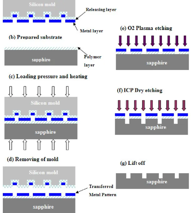
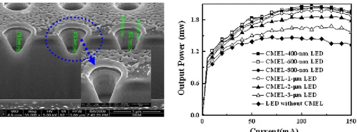
projected and de-magnified pattern exposure, but at the price of much higher equipment cost and lower throughput. In our work, we apply a novel contact-printing lithography, as schematically shown in Fig. 1, on fabricating patterned sapphire substrates (PSS) used in light-emitting-diodes (LEDs). This contact printing lithography method can directly transfer a metal film pattern from a silicon mold to a sapphire substrate, and subsequently use the transferred metal film pattern as the etching mask for inductively coupled plasma (ICP) etching on the sapphire substrate. The strength of this new approach lies on its capability of achieving sub-micrometer or nanometer-scaled patterning in a direct, easy, and large-area way as well as for obtaining deeper etching depth on sapphire because of excellent etching selectivity of metal films. Experiments have been carried out to demonstrate the feasibility of using this new approach for obtaining sub-micrometer surface structures on the complete surface area of a 2” sapphire substrate, as displayed in Fig. 2. This direct metal contact printing lithography had also been applied on red AlGaInP LEDs for opening a hole-array pattern on the top window layer of an AlGaInP LED. This patterned surface micro-structures with various sizes ranging from 400 nm to 3 um can effectively enhancing the light extraction efficiency of the LEDs. Experiments have been carried out and the results are shown in Fig. 3. An 23% increase of light-extraction efficiency was observed with a 400 nm diameter hole-array pattern.
Research Express@NCKU - Articles Digest
Fig. 1. A schematic diagram for the procedures of direct metal contact printing lithography for fabricating sub-micrometer surface structures on a sapphire substrate.
Fig. 2. A photo of a 2” sapphire wafer patterned with a 70 nm thick Cr film (left) and the SEM image of ICP patterned surface structures on the sapphire substrate (right).
Research Express@NCKU - Articles Digest
Fig. 3. Applying direct metal contact printing lithography to AlGaInP LEDs for opening a hole-array pattern on the top window layer (left) and enhanced light extraction efficiency of the LEDs (right).