Temperature effect on impact ionization characteristics in metamorphic
high electron mobility transistors
Po-Hsien Lai, Ssu-I Fu, Ching-Wen Hung, Yan-Ying Tsai, Tzu-Pin Chen, Chun-Wei Chen, and Wen-Chau Liua兲
Institute of Microelectronics, Department of Engineering, National Cheng-Kung University, 1 University Road, Tainan, Taiwan 70101, Republic of China
共Received 26 August 2006; accepted 17 November 2006; published online 26 December 2006兲 Comprehensive studies of temperature-dependent gate-metal-related impact ionization in metamorphic high electron mobility transistors共MHEMTs兲 are demonstrated. It is known that, from experimental results, the electric field and temperature dependences of impact ionization mechanisms in MHEMT’s operation are dominated by the ionization threshold energy and hot electron population. The peak impact ionization-induced gate current could be substantially decreased by the presence of specific gate contact with a higher Schottky barrier height. Therefore, the suppressions of bell-shaped behavior and related impact ionization effect are observed by using the appropriate Schottky gate contacts. © 2006 American Institute of Physics.
关DOI:10.1063/1.2410233兴
Recently, the metamorphic high electron mobility tran-sistors, MHEMTs共InP based layers on GaAs substrate兲, have attracted considerable attention for high power and low noise microwave applications.1,2 From the physical point of view, the increased gate leakage current as well as decreased breakdown voltage are mainly caused by the carrier genera-tion within the channel and carrier transport across the Schottky barrier layer.3,4Thus, the carrier generation through effective impact ionization in the channel layer is responsible for the breakdown characteristics.
Since the impact ionization is inversely proportional to the band gap value, the narrow band gap of InGaAs channel makes it susceptible to induce the impact ionization effect.3 This problem usually leads to the deteriorated device char-acteristics including the low breakdown voltage, high gate leakage current, and high output conductance. The extraction of impact ionization-induced gate current from the total mea-sured gate current becomes essential to study the impact ion-ization effect. It is noticeable that the impact ionion-ization effect strongly depends on the Schottky barrier height of gate con-tacts. The adequate determination of gate metals can sup-press the impact ionizations and then improve the device characteristics. In this work, the temperature-dependent char-acteristics of gate-metal-related impact ionizations in MHEMTs are investigated. This temperature effect on gate-metal-related impact ionization has never been found in pre-vious reports. Different metals, including Pt/ Au, Ti/ Au, and Au, as the Schottky gate contacts are fabricated simulta-neously to study the impact ionization effects. In order to consider the impact ionization-induced gate current, the con-venient excess gate hole current model established by Web-ster et al. is employed.4 Besides, two distinct mechanisms 共ionization threshold energy and hot electron population兲 for impact ionization, which separately dominate in different field ranges, are also presented to interpret the anomalous electric field and temperature dependences.
The MHEMT layer structure is similar to the previous work.5Drain-source Ohmic contacts were formed on the top
of cap layer by rapid thermal annealing of AuGe/ Ni/ Au metallurgy. Gate recess etching of cap layer was done by highly selective pH-adjusted succinic acid solution. For comparison, gate Schottky contacts were achieved by evapo-rating Pt/ Au 共20nm/130 nm兲, Ti/Au 共20nm/130 nm兲, and Au共150 nm兲, three kinds of different metals, for devices A, B, and C, respectively, on the Schottky barrier layer by using the same process sequence. Finally, the active structure un-derneath the gate feeder was completely removed by wet chemical etching to build the air-bridge gate structure which included multiple piers under the gate-feeder metal.6 The gate dimension was 1⫻100m2.
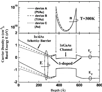
Figure1shows the schematic band diagrams and calcu-lated electron densities within channel layer regimes at ther-mal equilibrium. Experimentally, the measured Schottky bar-rier height⌽Bvalues of devices A, B, and C are 0.91共0.82兲,
0.78共0.71兲, and 0.71 共0.63兲 eV at 300 共480兲 K, respectively.
a兲Electronic mail: wcliu@mail.ncku.edu.tw
FIG. 1. Schematic band diagrams and calculated electron densities within channel layer regimes of the studied In0.46Ga0.54As/ In0.42Al0.58As MHEMTs with different Schottky gate metals.
APPLIED PHYSICS LETTERS 89, 263503共2006兲
0003-6951/2006/89共26兲/263503/3/$23.00 89, 263503-1 © 2006 American Institute of Physics Downloaded 13 Nov 2008 to 163.28.112.100. Redistribution subject to AIP license or copyright; see http://apl.aip.org/apl/copyright.jsp
Obviously, due to the increase of Schottky barrier height, the electron concentrations are decreased for devices A and B. Hence, the generation of electron-hole pairs and related im-pact ionization effect is effectively suppressed.2 The pres-ence of large conduction band discontinuity共⌬EC兲 between
InAlAs Schottky and InGaAs channel layers also substan-tially suppresses electrons injecting into the gate. This cer-tainly further improves the carrier confinement capability at higher temperature. The measured common-source I-V char-acteristics at different temperatures are illustrated in Fig. 2共a兲. The corresponding drain saturation current 共IDS兲 and transconductance共gm兲 versus gate-source voltage 共VGS兲
is shown in Fig.2共b兲. It should be noted that the kink effects or other degenerative behaviors caused by the impact ioniza-tion are not observed in the studied devices in the tempera-ture of 300– 480 K. Based on the significant suppression of leakage current, caused by the presence of wide-gap and high-resistivity undoped InAlAs Schottky and buffer layers, good pinch-off and saturation characteristics could be achieved in the studied devices. In particular, for device A, the drain current IDis not compressed significantly; even the VGSis increased up to +0.5 V. Furthermore, device A shows the relatively lower drain-source saturation current IDSS
共374 mA/mm at VGS= 0 V兲 at 300 K. This is because the
Pt/ Au gate metals共device A兲 lead to the increase of Schottky barrier height.2 This may considerably extend the depletion region beneath the gate and result in the reduced IDSS.
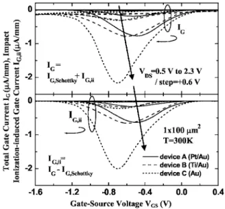
Figure 3 shows the total gate current 共IG兲 and impact
ionization-induced gate current共IG,ii兲 vs gate-source voltage 共VGS兲 under different electric field 共VDS兲 at 300 K. Also, the
evolutions of IG and IG,ii vs VGS under high electric fields 共VDS= + 2.0 V兲, at 300–480 K, are shown in Fig.4. Clearly,
the bell-shaped behavior reflects the preponderance of the impact ionization at high VDS and low temperature over the
Schottky gate leakage current. The existence of the bell-shaped behavior is caused by the impact ionization which requires both the conditions of significantly high electron concentration and high electric field.4 Since the gate deple-tion region is extended under higher 兩VGS兩 regimes 共more
negative bias兲, this reduces the electron concentration in the channel. On the contrary, even though the electron concen-tration is high at lower 兩VGS兩 regimes 共near zero bias兲, the
electric field is decreased. As a result, it is hard to find the FIG. 2.共a兲 Typical common-source I-V characteristics at different
tempera-tures.共b兲 Drain saturation current 共IDS兲 and transconductance 共gm兲 vs gate-source voltage共VGS兲 at different temperatures. The biased voltage is fixed at VDS= + 2.0 V.
FIG. 3. Total gate current共IG兲 and impact ionization-induced gate current 共IG,ii兲 vs gate-source voltage 共VGS兲 under different drain-source voltages 共VDS兲 at room temperature.
FIG. 4. Total gate current共IG兲 and impact ionization-induced gate current 共IG,ii兲 vs gate-source voltage 共VGS兲 at different temperatures. The biased voltage is fixed at VDS= + 2.0 V.
263503-2 Lai et al. Appl. Phys. Lett. 89, 263503共2006兲
impact ionization within these two regimes. However, at moderate兩VGS兩 regimes, both the electron concentration and
electric field are substantially increased. The electron-hole pairs are generated in the high electric field region between the gate and drain electrodes. Also, a portion of the holes is injected across the Schottky layer and collected by the gate terminal. Therefore, the gate hole current and related bell-shaped behavior are increased and occurred simultaneously, as indicated in Figs.3and4. The total gate current is com-posed of the hole current component, due to impact ioniza-tion occurring in the channel, and the Schottky leakage cur-rent component. According to the gate hole curcur-rent model, the IG,ii can be expressed as:4
IG,ii= IG− IG,Schottky, 共1兲
where IG,Schottkyis the Schottky gate leakage current, which is
a function of both the gate and drain voltages. Clearly, the bell-shaped behaviors, caused by the impact ionizations, of devices A and B are significantly suppressed as compared with that of device C. Even operating under higher electric field of VDS= + 2.3 V at 300 K, as shown in Fig. 3, the re-duced peaks IG,ii of −0.63 and −0.66A / mm are obtained
for devices A and B. These values are lower than that of device C共−2.01A / mm兲. This is caused by the evaporation of specific gate contacts, e.g., Pt/ Au and Ti/ Au. These higher Schottky barrier heights will lead to the substantial change of potential energy. This indeed extends the channel depletion region beneath the gate and results in the decrease of drain current in the channel. Therefore, the impact ioniza-tion effect can be effectively suppressed. Especially, it is found that the peaks IG,ii of devices A and B shift toward more positive VGSregimes over wide operating temperatures ranging from 300 to 480 K, as shown in Fig.4. Due to the increased phonon scattering with increasing the temperature, the electron mobility and drain current are decreased. Hence, because the peak IG,iiis dominated by the drain current den-sity under the identical electric field, the兩VGS兩 magnitudes of
devices A and B are needed to decrease to maintain the same drain current density.
The corresponding reverse evolutions of IG,ii between
the electric field共VDS兲 and temperature dependences are ob-served. This indicates that the electric field and temperature dependences of impact ionization mechanisms are different. Thus, it is important to understand and determine the domi-nant mechanism in different field regimes. Practically, the electric field and temperature dependences of impact ioniza-tion in device operaioniza-tion are mainly determined by the com-petition between the ionization threshold energy and hot electron population.7As shown in Fig. 3, with the decrease of the electric field共lower VDSbias兲, the impact ionization is
dominated by the high ionization threshold energy. Because electrons are distributed under relatively cool status, the hot electron population is substantially reduced at low electric
field. This leads to the absence of impact ionization in the channel as well as the reduced IG,ii. In contrast, since the
high electric field is presented in the gate-drain region at high VDS bias, electrons acquire enough energies, and it is
easy for the hot-electron-assisted impact ionization to take place in the channel layer. Subsequently, the related electron-hole pairs are generated which lead to the increase of IG,ii.
On the other hand, as shown in Fig.4, once the temperature is increased from 300 to 480 K, the ionization threshold en-ergy and related band gap are slightly decreased which tend to enhance the impact ionization effect. However, the mean free paths of channel electrons are significantly decreased due to the increased phonon scattering.8This indicates that it is hard to release lattice electrons with the insufficient en-ergy. Thus, the hot electron population and the corresponding impact ionization are substantially suppressed though the ionization threshold energy is slightly decreased. Simulta-neously, an overall decrease of IG,ii with increasing the
tem-perature is observed. This experimental result is in good agreement with the observations of Tan et al.,7 who argued that the ionization coefficient in In0.53Ga0.47As material is
decreased with increasing the temperature 共20–300 K兲 at high electric field.
In conclusion, the gate-metal-related impact ionizations in MHEMTs have been investigated. The influences of Schottky barrier height on the impact ionization effect and device performance are also studied. Further, two distinct mechanisms, which separately dominate the impact ioniza-tion in different field regimes, are proposed to interpret the anomalous electric field and temperature dependences. As a result, by using the higher Schottky barrier height of gate metals, both the bell-shaped behavior and related impact ion-ization effect are significantly suppressed. Also, the impact ionization-induced gate current is decreased with reducing the electric field and/or increasing the temperature.
Part of this work was supported by the National Science Council of the Republic of China under Contract No. NSC-95-2221-E-006-434-MY2.
1W. C. Hsu, Y. J. Chen, C. S. Lee, T. B. Wang, Y. S. Lin, and C. L. Wu, IEEE Electron Device Lett. 26, 59共2005兲.
2M. K. Hsu, H. R. Chen, S. Y. Chiou, W. T. Chen, G. H. Chen, Y. C. Chang, and W. S. Lour, Appl. Phys. Lett. 89, 033509共2006兲.
3S. M. Sze, Physics of Semiconductor Devices, 2nd ed.共Wiley, New York, 1981兲, p. 44.
4R. T. Webster, W. Shangli, and A. F. M. Anwar, IEEE Electron Device Lett. 21, 193共2000兲.
5C. W. Chen, P. H. Lai, W. S. Lour, D. F. Guo, J. H. Tsai, and W. C. Liu, Semicond. Sci. Technol. 21, 1358共2006兲.
6W. S. Lour and C. Y. Lia, Semicond. Sci. Technol. 13, 796共1998兲. 7C. H. Tan, G. J. Rees, P. A. Houston, J. S. Ng, W. K. Ng, and J. P. R.
David, Appl. Phys. Lett. 84, 2322共2004兲. 8G. A. Baraff, Phys. Rev. 128, 2507共1962兲.
263503-3 Lai et al. Appl. Phys. Lett. 89, 263503共2006兲