行政院國家科學委員會專題研究計畫 期中進度報告
應用於幹細胞移植之新型透明質酸組織膠之研發--子計畫
三:以多光子激發於透明質酸組織膠中製造小血管與分子
影像分析(2/3)
期中進度報告(完整版)
計 畫 類 別 : 整合型 計 畫 編 號 : NSC 98-3111-B-006-004- 執 行 期 間 : 98 年 12 月 01 日至 99 年 11 月 30 日 執 行 單 位 : 國立成功大學工程科學系(所) 計 畫 主 持 人 : 陳顯禎 共 同 主 持 人 : 謝式洲 報 告 附 件 : 出席國際會議研究心得報告及發表論文 處 理 方 式 : 本計畫可公開查詢中 華 民 國 100 年 01 月 07 日
行政院國家科學委員會補助專題研究計畫
□成果報告
■期中進度報告
以多光子激發於透明質酸組織膠中
製造小血管與分子影像分析
計畫類別:整合型計畫
計畫編號:
NSC 98-3111-B-006 -004
執行期間:
98 年 12 月 01 日至 99 年 11 月 31 日
執行機構及系所:
國立成功大學 工程科學系
計畫主持人:
陳顯禎
共同主持人:
謝式洲
計畫參與人員:
蘇園登、卓粳佶、連啟翔、陳盈婷、謝永達
成果報告類型(依經費核定清單規定繳交):完整報告
本計畫除繳交成果報告外,另須繳交以下出國心得報告:
出席國際學術會議心得報告
處理方式:
除列管計畫及下列情形者外,得立即公開查詢
中 華 民 國 100 年 01 月 07 日
目 錄
中文摘要……….………3
Abstract………3
1. Introduction………..………4
2. Sample preparation and microfabrication setup………..………5
2.1. Sample preparation………..………6
2.2. Femtosecond laser microfabrication system……….………...7
2.3. Designing 3D freeform structures………....………...7
3. Experimental results and discussions………..……….………..…7
3.1. Wavelength selection in femtosecond laser microfabrication.………....………8
3.2. Selective AuNR reshaping by femtosecond laser...….……….………....………9
3.3. 3D microfabrication………...……...……....……….…10
4. Conclusions…..……….………11
Reference……….………11
摘 要
本 研 究 主 要 利 用 飛 秒 雷 射 激 發 光 起 始 劑 Rose Bengal (RB) 進 行 雙 光 子 聚 合 反 應 (two-photon polymerization,TPP)並製作出具金奈米柱(gold nanorods,AuNRs)之三維微米 polyacrylamide 結構。製 作中為了使 AuNRs 於三維結構裡面並保留其近紅外光波段之光電特性,研究中量測出光起始劑 RB 的 最大雙光子吸收(TPA)並使用此雷射波長進行實驗,由此不僅提高雙光子聚合效率同時避免激發 AuNRs 的縱向電漿共振模態造成表面電漿子(surface plasmons,SPs)振動產生光熱形變(photothermal reshaping) 的發生。以 AuNRs 的縱向電漿共振波長與低能量的雙光子激發(TPE) 其 AuNRs 之三維微米結構可得 到雙光子致光(two-photon luminescence,TPL) 影像,同時也可在三維結構裡設計圖樣利用稍高於 AuNR 光熱變形之閥值能量,進行光熱變形使其紅外線 SPs 特性消失,再藉由低能量掃描得到特定圖樣之 TPL 影像。
關鍵詞:雙光子激發、三維微製作、金奈米柱、生醫材料。
Abstract
In this study, three-dimensional (3D) polyacrylamide microstructures containing gold nanorods (AuNRs) were fabricated by two-photon polymerization (TPP) using Rose Bengal (RB) as the photoinitiator. To retain AuNRs in the 3D polymer microstructures, the laser wavelength was chosen for two-photon RB absorption for improved TPP efficiency, but not for enhancing the longitudinal plasmon resonance of AuNRs which may result in photothermal damage of AuNRs. After TPP processing, the laser wavelength was tuned for the longitudinal plasmon resonance and the laser power was increased to beyond the damage threshold of the AuNRs for reshaping the AuNRs into gold nanospheres. As a result, AuNRs in designated positions of the fabricated 3D microstructures can be achieved. Two-photon luminescence from the doped AuNRs can also act as contrast agent for the visualization of 3D polymer microstructures.
1. Introduction
Photopolymerization is a process which uses a combination of light with low molecular weight photoinitiators to trigger the polymerization reaction [1-3]. To fabricate three-dimensional (3D) microstructures, multiphoton excited (MPE) photochemistry can be used. Since multiphoton absorption is confined to the focal volume, photopolymerized structures with the desired 3D submicron features can be created [4-8]. This approach not only allows the creation of structures that cannot be constructed by conventional single-photon lithography, but also provides greater spatial resolution than other 3D microfabrication techniques. Therefore, multiphoton photopolymerization has attracted widespread interest owing to its potential use in fabricating intrinsic 3D microstructures with sub-diffraction limited spatial resolution [4]. The utilization of short pulse width and tight focusing are critical for inducing sufficient extent of two-photon absorption (TPA) and for achieving high precision fabrication. For the work presented hereafter, a femtosecond titanium-sapphire (ti-sa) laser was as the excitation source. Previously, femtosecond 3D microfabrication has been demonstrated in resin- [3,4,9,10], protein- [2], silica- [11], and metal-substrates [12,13]. In additional, photonic crystals have also been demonstrated to be photopolymerizable by TPA [14-16].
Among the developed nanomaterials for biomedical applications, gold nanoparticles (AuNPs) are particularly attractive due to their biocompatibility. Since biomedical applications often involve 3D specimen manipulation, near infrared (NIR) light is preferred due to its optimal tissue transmission from reduced scattering and energy absorption. As a result, maximum irradiation penetration through tissue and minimization of the auto-fluorescence of non-target tissue can be achieved [17]. Therefore, there have been efforts aiming at shifting the surface plasmon resonance of AuNPs into the NIR region for potential biological applications [18,19]. Numerous NIR-absorbing, Au-based bionanomaterials have been developed. Specifically, Au nanorods (AuNRs) with different aspect ratios and corresponding longitudinal plasmon resonance in the 700 to 1000 nm fall within the spectral range of the femtosecond ti-sa laser. AuNRs designed with these properties have been applied in localized surface plasmon resonance light scattering [20], Rayleigh elastic scattering [21], surface-enhanced Raman inelastic scattering [22], optical coherent tomography scattering [23], two-photon luminescence (TPL) imaging [24], and photothermal therapy [17-19].
While AuNRs have found wide biomedical applications, the use of AuNRs in microfabrication has been rare. Due to the fact that metallic nanoparticles-polymer composites exhibit unique electrical, optical, and mechanical properties, in this work, we explored these properties for microfabrication. Specifically, multiphoton photopolymerization using acrylamide as a reactive monomer, Rose Bengal (RB) as a photoinitiator, triethanolamine (TEA) as co-initiator, dimethyl sulfoxide (DMSO) as surfactant, and AuNRs were used to direct the 3D assembly of polymer microstructures. We present the first example of 3D polymer microstructures containing two-photon excitable AuNRs from the minimally-damped surface plasmon resonance effects [24-26]. We improved the fabrication efficiency at a threshold laser power without damage to the AuNRs by mixing a suitable content with acrylamide, RB, TEA, DMSO, and AuNRs. Moreover, an optimal laser wavelength was chosen for RB TPA, but not for AuNR absorption. Furthermore, the selectivity of AuNRs with different aspect-ratios in different locations can be implemented by photothermal reshaping [27]. Herein, a higher laser power, greater than the threshold of the AuNR damage at the wavelength for the AuNR absorption, was adopted to reshape the AuNRs at the designated positions. The experimental results demonstrate that the developed 3D polymer microstructures containing the AuNRs not only improves efficiency by decreasing the power density of the femtosecond laser, but also provides a great diversity of
optical properties that can act as attractive contrast agents for TPL imaging in 3D fabricated microstructures. We will also demonstrate that the TPL from doped AuNRs can be used for internal diagnosis of 3D polymer microstructures.
2. Sample preparation and microfabrication setup
2.1. Sample preparation
Hydrogen tetrachloroaurate (III) hydrate (HAuCl4) was purchased from Alfa Aesar Co. (Ward Hill, MA,
USA). Cetyltrimethylammonium bromide (CTAB), ascorbic acid, sliver nitrate, sodium
Electron micrographs of the AuNRs using transmission electron microscopes (TEM) (Jeol 1200, at 80 kV; Jeol 3010, at 300 kV; and Philips CM-200, at 200 kV, Japan) were obtained by placing a drop of the sample on a copper mesh coated with an amorphous carbon film. After evaporation of the solvent was in a vacuum desiccator, the samples were placed on ITO-coated glass slides for the specimen characterization using a scanning electron microscope (SEM) (Jeol 7000). The UV/Vis absorption spectra were recorded on a spectrometer (Agilent 8453, USA), while the Fourier transform infrared (FTIR) spectra were collected using another spectrometer (PerkinElmer RX1, USA). Finally, the data of zeta potential were measured using a spectrometer (Manern Nano-ZS90, UK).
tetrahydrdoborate, acrylamide, bis-acrylamide, RB, TEA, and DMSO were purchased from Sigma-Aldrich Co. (St. Louis, MO, USA). All chemicals and reagents were of the analytical grade. AuNRs were synthesized using the seedless growth method [17-19,28,29]. The mean length and width of the AuNRs were approximately 40.2 nm and 11.2 nm, respectively, and their aspect ratio (length divided by width) was about 3.6. A resin, acrylamide/bis-acrylamide (74:1), was utilized as a reactive monomer. The fabrication solution is consisted of 2.0 mM RB solution (photoinitiator), 0.1 M TEA solution (co-initiator), and 10% (v/v) DMSO (surfactant) mixed into the monomer solution.
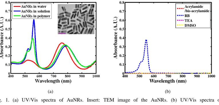
AuNRs with a CTAB surfactant coating were synthesized using the seedless growth method. Due to the presence of CTAB, the surface charge of the AuNRs revealed a zeta potential of approximately 39.2 mV. As shown in Fig. 1(a), AuNRs exhibit two plasmon resonances with a transverse plasmon (about 520 nm in water) and a longitudinal plasmon (about 760 nm in water; 780 nm in the fabrication solution and the polymer). Also shown in Fig. 1(a) is the TEM image of the AuNRs demonstrating that these materials have an aspect ratio of approximately 3.6 (length: 40.2 nm, width: 11.2 nm). On the other hand, the absorption spectrum of RB exhibited one main peak at around 550 nm (Fig. 1(b)), while a similar band appeared as the RB was added to the fabrication solution with the AuNRs (Fig. 1(a)). However, UV/Vis spectra results in Fig. 1(a) show that there were no apparent differences in the longitudinal plasmon of the AuNRs despite decrease in the RB absorption after the polymerization of acrylamide. Shown in Fig. 1(b) are the absorption spectra of acrylamide/bis-acrylamide, aqueous RB, TEA, and DMSO (concentrations of the RB in Figs. 1(a) and 1(b) are both 2.0 mM). Since the spectra in Fig. 1(a) including the transverse plasmon effect of the AuNRs, the absorbance at around 550 nm in Fig. 1(a) is higher than that in Fig. 1(b).
4000 500 600 700 800 900 1000 0.1 0.2 0.3 0.4 0.5 0.6 0.7 0.8 Wavelength (nm) Abso rba nc e ( A. U. ) Acrylamide /bis-acrylamide RB TEA DMSO (a) (b)
Fig. 1. (a) UV/Vis spectra of AuNRs. Insert: TEM image of the AuNRs. (b) UV/Vis spectra of acrylamide/bis-acrylamide, aqueous RB, pure TEA, and DMSO.
2.2. Femtosecond laser microfabrication system
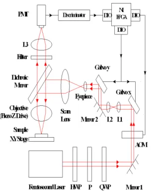
Shown in Fig. 2 is the schematic of the femtosecond laser fabrication system. Key components of our instrument include a femtosecond laser (Tsunami, Spectra-Physics, USA), an inverted optical microscope (Axiovert 200, Zeiss, Germany), galvanometer x-y scanner (6215H, Cambridge, USA), a triple-axis sample positioning stage (ProScanTM
The real-time FPGA DAQ card based on our custom LabVIEW program can synchronously control the instrument through interfaces constructed in-house. To achieve a fast and precise scan, the digital and analog I/O signal from the programming FPGA was utilized. A digital I/O via a voltage converter is connected into the AOM for fast on/off laser control, with a speed of up to 9 MHz. The voltage converter reduces the 3.3 V command signal from the FPGA digital input/output to below 1.0 V to match the requirement of the AOM driver. The SPC-based pulse counting scheme is based on the FPGA digital input/output. Specifically, the number of high to low electronic transitions signals from a discriminator-processed PMT was determined. The
II, Prior, UK), a z-axis piezoelectric nano-positioning stage (Nano-F100, Mad City Labs, USA), an acousto-optic modulator (AOM) (23080-x-1.06-LTD, Neos, USA), photomultiplier tubes (PMTs) (H5783P, Hamamatsu, Japan), and a data acquisition (DAQ) card with a field-programmable gate array (FPGA) module (PCI-7831R, National Instruments, USA). The femtosecond ti-sa laser source has a pulse width of less than 100 fs and a repetition rate of 80 MHz. The FPGA module was designed to perform a number of simultaneous tasks including control of the galvanometer scanner and the z-axis piezoelectric stage for 3D focal spot positioning; modulating the AOM for rapid on/off switching of the laser and pulse selection; and processing of the single photon counting (SPC) signals. Selected experimental parameters such as laser power, scanning rate, imaging, and sample positioning can be adjusted by the use of custom LabVIEW program and electronics interfaces. In this manner, imaging with nonlinear optical signals (two-photon fluorescence (TPF)/second harmonic generation (SHG)) and 3D microfabrication can be achieved. To overcome the group velocity dispersion of the femtosecond laser through the AOM and the objective, an SF-10 prism pair (PC-TS-KT, Newport, USA) was used for optimized laser operation in the wavelength region between 700 to 840 nm [30].
pulse counter records one count when the voltage level underwent a high to low transition. The highest operating frequency of our FPGA module is 200 MHz, which is sufficient for determining the processing signals associated with our 80 MHz femtosecond laser source.
Fig. 2. The optical setup and control scheme of the femtosecond laser imaging and microfabrication system.
2.3. Designing 3D freeform structures
In addition to nonlinear optical imaging capabilities, CAD software such as AutoCAD, Pro/E, and Solidworks can be used to design 3D structures for microfabrication. To transform 3D structures into 2D processing patterns, transformation programs such as Rhino and Materialse Magics can be adopted to convert the 3D structures into sequential 2D DXF files [31]. The 2D DXF files are then converted into bitmap files and downloaded into the FPGA module as laser processing commands. With the use of 3D structure design, we were able to create the desired structures.
3. Experimental results and discussions
With the fabrication solution consisting of acrylamide/bis-acrylamide, RB, TEA, DMSO, and AuNRs, we were able to improve the polymerization efficiency. More than 1.0 mM of the RB was required to provide adequate photoinitiation processing, while the DMSO surfactant is for the uniform dissolution of TEA. The AuNRs with sufficient CTAB can be dissolved in the fabrication solution. In order to implement the multiphoton fabrication of 3D polymer microstructures without femtosecond laser damage to the AuNRs, it is important to adopt a fabrication laser power as low as possible with a wavelength appropriate for the RB TPA, but not for the AuNR absorption. After multiphoton fabrication, the selectivity of AuNRs with different aspect-ratios in different locations can be achieved by photothermal reshaping. Moreover, a higher laser power, greater than the threshold of the AuNR damage and at the resonance wavelength of their longitudinal plasmon, was utilized to reshape the AuNRs into Au nanospheres. As a result, the existence of the AuNRs in designated positions of the fabricated microstructures can be achieved.
3.1. Wavelength selection in femtosecond laser microfabrication
In TPP processing, we can improve the polymerization efficiency of the acrylamide/bis-acrylamide monomer by adopting the laser wavelength at the maximum TPA of the photoinitiator, RB. Upon excitation, the time-averaged TPF photon count (F) of a fluorescence species is proportional to the cross section (δ) of TPA and can be given as [32]
2 2 1 8 2 p g nP F C f δη φ τ πλ ≈
,
(1)where η2 is the quantum efficiency of TPF, φ the fluorescence collection efficiency of the detection system, C the concentration of the photoinitiator, gp the dimensionless quantity for the degree of the second-order temporal coherence, f the pulse repetition rate, τ the excitation pulse width at full-width at half maximum, n the refractive index of the measurement medium, P the average incident power, and λ the excitation wavelength. The excitation pulse widths can be maintained at different excitation wavelengths after the SF-10 prism pair compensation. The TPA can be represented by δ × η2
2 F
.
δη
∝λτ
, and based on the measured TPF photon count, the measured excitation pulse width, and the excitation wavelength. Hence, the TPA (probability) can be expressed as
(2)
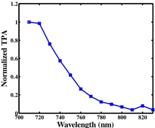
In TPA spectrum measurement experiment, the TPF photon counts were collected by the PMTs via the SPC module at the x galvanometer scanner rate of 20 kHz and the average excitation power of 10.0 mW. The excitation spectral range was selected from 710 to 830 nm and the pulse widths at different wavelengths after the objective were monitored by an in-lab constructed autocorrelator. The relative TPA spectrum of the RB (2.0 mM) in DI water as a function of the excitation wavelength is shown in Fig. 3. It was found that within the excitation wavelengths we examined, the excitation wavelength corresponding to the maximum value of the relative TPA of the RB was between 710 and 720 nm. Therefore, a fabrication laser wavelength of around 720 nm was adopted. Moreover, in order to implement the multiphoton fabrication of 3D polymer microstructures with AuNRs, the wavelengths of the two plasmon resonances of the adopted AuNRs should differ significantly from the fabrication wavelength of 720 nm. As shown in Fig. 1(a), the AuNRs with an aspect ratio of approximately 3.6 exhibits two plasmon resonances with transverse plasmon at around 520 nm and longitudinal plasmon at 780 nm in the fabrication solution. However, the AuNRs with a longitudinal plasmon wavelength longer than 780 nm are also good candidates for the 3D multiphoton fabrication process with the RB.
7000 720 740 760 780 800 820 0.2 0.4 0.6 0.8 1 1.2 Wavelength (nm) N or mal iz ed TP A
Fig. 3. TPA spectrum of RB as function of excitation wavelength.
3.2. Selective AuNR reshaping by femtosecond laser
In order to implement multiphoton fabrication of 3D polymer microstructures, the power of the 100 fs femtosecond laser at the repetition rate of 80 MHz must be sufficient to support the MPE photochemistry process. According to our experience, the use of NA 1.3 objective and the x-galvanometer scan rate of 1 kHz, the laser power at the TPA wavelength of the photoinitiator must be controlled to within at least a few mW to implement the multiphoton fabrication in our solution. Furthermore, since AuNRs can be easily reshaped by utilizing the 100 fs laser at the resonance wavelength of the longitudinal plasmon of the AuNRs, the threshold power for completely melting AuNRs within a linearly polarized (along the longitudinal axis of the AuNRs) laser pulse was about 0.96 mW [33]. However, from the simulation results based on a two-temperature model, the threshold power for the 100 fs linearly polarized laser at the resonance wavelength is 0.049 mW [34]. When the polarization of the laser is turned from linear to circular, the threshold power can be decreased half. Also, the orientation-specific damage for the long axis of AuNRs parallel to the direction of the linearly polarized laser can be avoided. From our results, the threshold power for AuNR melting using the circularly polarized, femtosecond laser at the resonance wavelength was 0.5 mW. This laser power would result in the minimal damage of AuNR for all of the orientations. Based on the AuNR absorption spectra in Fig. 1(a), the minimum AuNR damage power at the RB TPA wavelength of around 720 nm can be several times higher than 0.5 mW, the power used in processing the AuNRs at the longitudinal plasmon resonance wavelength of 780 nm.
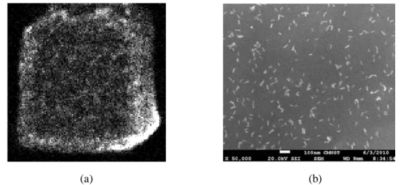
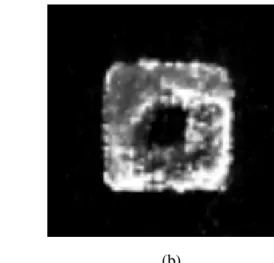
In our experiments, a quarter wave plate (QWP) was inserted after the linear polarizer (Fig. 2). The fabrication laser power of 1.0 mW at the optimal fabrication wavelength of 720 nm was used (RB concentration 2.0 mM) [35]. Due to the generation of highly efficient TPL, the AuNRs can be attractive contrast agents for imaging 3D fabricated microstructures. Therefore, we examined the tomographic profile of the AuNRs filled fabricated microstructure by TPL imaging. Fig. 4(a) shows the TPL image of a fabricated 10 x 10 μm2
square polymer microstructure filled with AuNRs. In this study, TPL images were excited by the use of 0.1 mW, 100 fs laser at 780 nm and a scan rate of 20 kHz. The SEM zoom in image shows clear and intact AuNRs inside the polyacrylamide (Fig. 4(b)). These results indicate that there was no change to the morphology of the AuNRs after the femtosecond laser fabrication process, even when 1.0 mW fabrication laser power was used. It is likely that most of the laser energy was dissipated into the RB for
photopolymerization, not for AuNR absorption.
(a) (b)
Fig. 4. A 10 x 10 μm2 square polymer microstructure with AuNRs imaged with (a) TPL and (b) SEM. The 780 nm AuNRs with different orientations in the 3D polymer microstructures can be selectively processed in designated positions via the photothermal reshaping mechanism. For this purpose, the ti-sa wavelength was tuned to 780 nm, the longitudinal plasmon resonance of the AuNRs, and circularly polarized laser was adopted to reshape the AuNRs in all of the orientations. To completely reshape the AuNRs, the laser power was increased to 5.0 mW. Fig. 5(a) shows the cross TPL image of the fabricated AuNR-doped microstructure (Fig. 4(a)) after photothermal reshaping to destroy the AuNRs outside of the cross pattern. The TPL image was acquired under the same imaging condition as in Fig. 4(a). The SEM zoom in image indicates that the AuNRs were completely reshaped into spherical AuNPs at 5.0 mW (Fig. 5(b)).
(a) (b)
Fig. 5. Cross pattern of AuNRs created by photothermal reshaping acquired with (a) TPL and (b) TEM.
3.3. 3D microfabrication
For 3D microfabrication, the sequential 2D bitmap files sliced from a 3D CAD model were downloaded into the FPGA to control the laser illumination via the AOM. Since TPP is confined to the focal volume, 3D freeform polymer solid structures can be developed. Unreacted solution was then washed out by water. Fig. 6(a) shows the TPL image of a hollow 3D microstructure by utilizing the fabrication and imaging conditions described in Sec. 3.2. The structure has a base area of 20 x 20 μm2 and a height of 5 μm. Finally, the diameter of the hole was 10 μm and the distance between two adjacent axial layers was 0.1 μm. Fig. 6(b) is the cross-sectional image of the base of the microfabricated structure of Fig. 6(a). The fabrication spatial
resolution of the 3D polyacrylamide microstructure we achieved is not as fine as ethoxylated trimethylolpropane triacrylate polymerization microstructures [31]. However, the water soluble acrylamide monomers were uniformly mixed with AuNR. Moreover, the polyacrylamide material is biocompatible, and therefore ready for bioapplications.
(a) (b)
Fig. 6. 3D TPP microstructure imaged by (a) 3D TPL (Insert: 2D bright-field image) and (b) 2D TPL image of the microstructure in (a) at the base.
4. Conclusions
The biocompatible 3D microstructure of polyacrylamide with AuNRs was fabricated via the TPP processing. To avoid AuNRs damage in the 3D microstructures, the fabrication laser wavelength (at 1.0 mW) was tuned for RB TPA, not for longitudinal plasmon resonance. Furthermore, a 5.0 mW laser power at the wavelength for the longitudinal plasmon resonance was adopted to reshape the AuNRs into AuNPs in designated positions within the 3D microstructures. Furthermore, doped AuNRs within TPL act as a contrast agent for internal visualization of the fabricated 3D microstructures. The approach described in this work can be used to create microstructures for biomedical applications.
References
1. C. R. Lambert, I. E. Kochevar, and R. W. Redmond, “Differential reactivity of upper triplet states produces wavelength-dependent two-photon photosensitization using Rose Bengal,” J. Phys. Chem. B 103,
3737-3741 (1999).
2. J. D. Pitts, P. J. Campagnola, G. A. Epling, and S. L. Goodman, “Submicron multiphoton free-form
fabrication of proteins and polymers: studies of reaction efficiencies and applications in sustained release,” Macromolecules 33, 1514-1523 (2000).
3. P. J. Campagnola, D. M. Delguidice, G. A. Epling, K. D. Hoffacker, A. R. Howell, J. D. Pitts, and S. L. Goodman, “3-dimensional submicron polymerization of acrylamide by multiphoton excitation of xanthene dyes,” Macromolecules 33, 1511-1513 (2000).
4. S. Kawata, H. B. Sun, T. Tanaka, and K. Takada, “Finer features for functional microdevices,” Nature 412, 697-698 (2001).
5. P. Galajda and P. Ormos, “Complex micromachines produced and driven by light,” Appl. Phys. Lett. 78, 249-251 (2001).
threshold material system,” Appl. Phys. Lett. 80, 312-314 (2002).
7. M. Miwa, S. Juodkazis, T. Kawakami, S. Matsuo, and H. Misawa, “Femtosecond two-photon stereo-lithography,” Appl. Phys. A: Mater. Sci. Process. 73, 561-566 (2001).
8. W. Denk, J. H. Strickler, and W. W. Webb, “Two-photon laser scanning fluorescence microscopy,” Science
248, 73-76 (1990).
9. T. Watanabe, M. Akiyama, K. Totani, S. M. Kuebler, F. Stellacci, W. Wenseleers, K. Braun, S. R. Marder, and J. W. Perry, “Photoresponsive hydrogel microstructure fabricated by two-photon initiated
Polymerization,” Adv. Funct. Mater. 12, 611-614 (2002).
10. Z. B. Sun, X. Z. Dong, W. Q. Chen, S. Nakanishi, M. Duan, and S. Kawata, “Multicolor polymer
nanocomposites: in situ synthesis and fabrication of 3D microstructures,” Adv. Mater. 20, 914-919 (2008). 11. A. Marcinkevicius, S. Juodkazis, M. Watanabe, M. Miwa, S. Matsuo, and H. Misawa, “Femtosecond
laser-assisted three-dimensional microfabrication in silica,” Opt. Lett. 26, 277-279 (2001).
12. P. W. Wu, W. C. Cheng, I. B. Martini, B. Dunn, B. J. Schwartz, and E. Yablonovitch, “Two-photon photographic production of three-dimensional metallic structures within a dielectric matrix,” Adv. Mater.
12, 1438-1441 (2000).
13. Y. Y. Cao, N. Takeyasu, T. Tanaka, X. M. Duan, and S. Kawata, “3D metallic nanostructure fabrication by surfactant-assisted multiphoton-induced reduction,” Small 5, 1144-1148 (2009).
14. N. Takeshima, Y. Narita, T. Nagata, and S. Tanaka, “Fabrication of photonic crystals in ZnS-doped glass,” Opt. Lett. 30, 537-539 (2005)
15. G. Zhou and M. Gu, “Direct optical fabrication of three-dimensional photonic crystals in a high refractive index LiNbO3
16. Z. B. Sun, X. Z. Dong, S. Nzkanishi, W. Q. Chen, X. M. Duan, and S. Kawata, “Log-pile photonic crystal of CdS-polymer nanocomposites fabricated by combination of two-photon polymerization and in situ synthesis,” Appl. Phys. A 86, 427-431 (2007).
crystal,” Opt. Lett. 31, 2783-2785 (2006).
17. W. S. Kuo, C. N. Chang, Y. T. Chang, M. H. Yang, Y. H. Chien, S. J. Chen, and C. S. Yeh, “Gold nanorods in photodynamic therapy, as hyperthermia agents and in near-infrared optical imaging,” Angew. Chem. Int. Ed. 49, 2711-2715 (2010).
18. W. S. Kuo, C. M. Wu, Z. S. Yang, S. Y. Chen, C. Y. Chen, C. C. Huang, W. M. Li, C. K. Sun, and C. S. Yeh, “Biocompatible bacteria@Au composites for application in the photothermal destruction of cancer cells,” Chem. Commun. 37, 4430-4432 (2008).
19. W. S. Kuo, C. N. Chang, Y. T. Chang, and C. S. Yeh, “Antimicrobial gold nanorods with dual-modality photodynamic inactivation and hyperthermia,” Chem. Commun. 32, 4853-4855 (2009)
20. J. Nappa, G. Revillod, J. P. Abid, I. Russier-Antoine, C. Jonin, E. Benichou, H. H. Giraultb, and P. F. Brevet, “Hyper-Rayleigh scattering of gold nanorods and their relationship with linear assemblies of gold nanospheres,” Faraday Discuss. 269, 935-939 (2004).
21. A. K. Singh, D. Senapati, S. Wang, J. Griffin, A. Neely, P. Candice, K. M. Naylor, B. Varisli, J. R. Kalluri, and P. C. Ray, “Gold nanorod based selective identification of Escherichia coli bacteria using two-photon Rayleigh scattering spectroscopy,” ACS Nano 3, 1906-1912 (2009).
22. Q. Liao, C. Mu, D. S. Xu, X. C. Ai, J. N. Yao, and J. P. Zhang, “Gold nanorod array with good reproducibility for high-performance surface-enhanced Raman scattering,“ Langmuir 25, 4708-4714 (2009).
23. L. Oldenburg, M. N. Hansen, D. A. Zweifel, A. Wei, and S. A. Boppart, “Plasmon-resonant gold nanorods as backscattering albedo contrast agents for optical coherent tomography, “ Opt. Express 14, 6724-6738 (2006).
24. N. J. Durr, T. Larson, D. K. Smith, B. A. Korgel, K. Sokolov, and A. Ben-Yakar, “Two-photon
luminescence imaging of cancer cells using molecularly targeted gold nanorods,” Nano. Lett. 7, 941-945 (2007).
25. M.B. Mohamed, V. Volkov, S. Link, and M. A. El-Sayed, “The 'lightning' gold nanorods: fluorescence enhancement of over a million compared to the gold metal,” Chem. Phys. Lett. 317, 517-523 (2000). 26. C. Sonnichsen, T. Franzl, T. Wilk, G. von Plessen, J. Feldmann, O. Wilson, and P. Mulvaney, “Drastic
reduction of plasmon damping in gold nanorods,” Phys. Rev. Lett. 88, 077402 (2002).
27. P. Zijlstra, J. W. M. Chon, and M. Gu, “Five-dimensional optical recording mediated by surface plasmons in gold nanorods,” Nature 459, 410-413 (2009).
28. N. R. Jana, L. Gearheart, and C. J. Murphy, “Evidence for seed-mediated nucleation in the chemical reduction of gold salts to gold nanoparticles,” Chem. Mater. 13, 2313-2322 (2001).
29. J. Perez-juste, I. Pastoriza-Santos, L. M. Liz-Marzan, and P. Mulvaney, “Gold nanorods: synthesis, characterization and applications,” Coordination Chem. Rev. 249, 1870-1901 (2005).
30. Z. Zhang and T. Yagi, “Observation of group delay dispersion as a function of the pulse width in as mode locked Ti:sapphire laser,” Appl. Phys. Lett. 63, 2993-2995 (1993).
31. L. P. Cunningham, M. P. Veilleux, and P. J. Campagnola, “Freeform multiphoton excited microfabrication for biological applications using a rapid prototyping CAD-based approach,” Opt. Express 14, 8613-8621 (2006).
32. C. Xu and W. W. Webb, “Measurement of two-photon excitation cross sections of molecular fluorophores with data from 690 to 1050 nm,” J. Opt. Soc. Am. B 13,481-491 (1996).
33. S. Link, C. Burda, B. Nikoobakht, and M. A. El-Sayed, “Laser-induced shape changes of colloidal gold nanorods using femtosecond and nanosecond laser pulses,” J. Phys. Chem. 104, 6152-6163 (2000). 34. O. Ekici, R. K. Harrison, N. J. Durr, D. S. Eversole, M. Lee, and A. Ben-Yakar, “Thermal analysis of gold
nanorods heated with femtosecond laser pulses,” J. Phys. D: Appl. Phys. 41, 185501 (2008).
35. C.-Y. Lin, K.-C. Chiu, C.-Y. Chang, S.-H. Chang, T.-F. Guo, and S.-J. Chen, “Surface plasmon-enhanced and quenched two-photon excited fluorescence,” Opt. Express 18, 12807-12817 (2010).
計畫成果自評
與本計畫完全相關成果:
2篇SCI論文
W.-S. Kuo, C.-H. Lien, K.-C. Cho, C.-Y. Chang, C.-Y. Lin, L. L. H. Huang, P. J. Campagnola, C. Y. Dong,* and S.-J. Chen*
C.-H. Lien, W.-S. Kuo, K.-C. Cho, Y.-D. Su, L. L. H. Huang, P. J. Campagnola, C. Y. Dong, and , “Multiphoton fabrication of freeform polymer microstructures with gold nanorods,” Optics Express, vol. 18, no. 26, pp. 27550-27559, December 2010. (Impact Factor: 3.880)
S.-J. Chen*
5 篇研討會論文
, “Gold nanorods-doped BSA microstructures via multiphoton excited photochemistry,” submitted to Optics Express (2010).
W.-S. Kuo, C.-H. Lien, K.-C. Cho, C.-Y. Chang, C.-Y. Lin, P. J. Campagnola and S.-J. Chen*
, “Three-dimensional polymer microdevices with gold nanorods,” Proc. SPIE, vol. 7757, no. 123, August 2010.
S.-J. Chen*
K.-C. Cho, C.-Y. Chang, and
, “3D plasmonic microdevices,” Optics and Photonics in Taiwan 2010, Tainan, Taiwan, December 2010. (Invited Talk)
S.-J. Chen*
C.-H. Lien, W.-S. Kuo, K.-C. Cho, and
, “Reverse-engineering femtosecond laser microprocessing for biotissues,” Optics and Photonics in Taiwan 2010, Tainan, Taiwan, December 2010.
S.-J. Chen*
, “Gold nanorods-doped BSA microstructures via
multiphoton excited photochemistry,” Optics and Photonics in Taiwan 2010, Tainan, Taiwan, December 2010.
S.-J. Chen*
與本計畫部分相關成果:
, “Fabrication of 3D plasmonic biomicrodevices,” ACP 2010, Shanghai, China, December 2010. (Invited Talk)
5篇SCI論文
R.-Y. He, C.-Y. Lin, Y.-D. Su, K.-C. Chiu, N.-S. Chang, H.-L. Wu, and S.-J. Chen*
W.-S. Kuo, C.-N. Chang, Y.-H. Chien, Y.-T. Chang,
, “Imaging live cell membranes via surface plasmon-enhanced fluorescence and phase microscopy,” Optics Express, vol. 18, no. 4, pp. 3649-3659, February 2010. (Impact Factor: 3.880)
S.-J. Chen
C.-Y. Lin
, and C.-S. Yeh, “Gold nanorods in photodynamic therapy, as hyperthermia agents, and in near-infrared optical imaging” Angewandte Chemie International Edition, vol. 49, no. 15, pp. 2711-2715, April 2010. (Impact Factor: 10.879)
, K.-C. Chiu, C.-Y. Chang, S.-H. Chang, T.-F. Guo, and S.-J. Chen*
Y.-D. Su, K.-C. Chiu, N.-S. Chang, H.-L. Wu, and
, “Surface plasmon-enhanced and quenched two-photon excited fluorescence,” Optics Express, vol. 18, no. 12, pp. 12807-12817, June 2010. (Impact Factor: 3.880)
S.-J. Chen*
V. Hovhannisyan, A. Ghazaryan, Y.-F. Chen,
, “Study of cell-biosubstrate contacts via surface plasmon polariton phase microscopy,” Optics Express, vol. 18, no. 19, pp. 20125-20135, September 2010. (Impact Factor: 3.880)
S.-J. Chen*, and C.-Y. Dong*
國際合作:
, “Photophysical mechanisms of collagen modification by 80 MHz femtosecond laser,” Optics Express, vol. 18, no. 23, pp. 24037-24047, November 2010. (Impact Factor: 3.880)
Cooperated with Prof. Paul J. Campagnola, University of Connecticut Health Center (UCHC) onto “Integrating Plasmonic methods into Multiphoton Excitation.” The PhD student, Mr. Ruei-Yu He, got the NSC grant and to study at UCHC for one year (08/2009-06/2010).
Cooperated with Prof. Peter So, MIT onto “Widefield Multiphoton Excited Fluorescence Microscopy with Adaptive Optics.” The PhD student, Mr. Keng-Chi Cho, got the NSC grant and to study at MIT for one year (08/2009-07/2010).
國科會補助專題研究計畫成果報告自評表
請就研究內容與原計畫相符程度、達成預期目標情況、研究成果之學術或應用價
值(簡要敘述成果所代表之意義、價值、影響或進一步發展之可能性)
、是否適
合在學術期刊發表或申請專利、主要發現或其他有關價值等,作一綜合評估。
1. 請就研究內容與原計畫相符程度、達成預期目標情況作一綜合評估
■ 達成目標
□ 未達成目標(請說明,以 100 字為限)
□ 實驗失敗
□ 因故實驗中斷
□ 其他原因
說明:
2. 研究成果在學術期刊發表或申請專利等情形:
論文:■已發表 □未發表之文稿 □撰寫中 □無
專利:□已獲得 □申請中 □無
技轉:□已技轉 □洽談中 □無
其他:
(以 100 字為限)
3. 請依學術成就、技術創新、社會影響等方面,評估研究成果之學術或應用價
值(簡要敘述成果所代表之意義、價值、影響或進一步發展之可能性)(以
500 字為限)
國科會補助計畫衍生研發成果推廣資料表
日期:100 年 01 月 07 日國科會補助計畫
計畫名稱:以多光子激發於透明質酸組織膠中製造小血管與分子 影像分析 計畫主持人:陳顯禎 計畫編號:NSC 98-3111-B-006 -004 學門領域::幹細胞/再生生 物研發成果名稱
(中文)無 (英文)成果歸屬機構
發明人
(創作人)
技術說明
(中文) (200-500 字) (英文)產業別
技術/產品應用範圍
技術移轉可行性及預期
效益
註:本項研發成果若尚未申請專利,請勿揭露可申請專利之主要內容。行政院國家科學委員會補助國內專家學者出席國際學術會議報告
99 年 8 月 09 日 報告人姓名 陳顯禎 服務機構 及職稱 國立成功大學工程科學系 教授 時間 會議 地點 自 99 年 07 月 31 日 迄 99 年 08 月 08 日 美國加州 San Jose City本會核定 補助文號 會議
名稱
(中文) 2010 SPIE Optics & Photonic (英文) 2010 SPIE 光電研討會 發表
論文 題目
(中文) 廣視域多光子激發螢光顯微術於活體動物之研究
(英文) Widefiled multiphoton excited florescence microcopy for animal study
in vivo
報告內容:
一、參加會議經過:2010 SPIE 光電研討會:8/01-8/05
2010 SPIE 光電研討會於 2010 年 8 月 01 日至 8 月 05 日於美國加州San Diego市盛
大舉行。參加人員來自世界各國與光電工程研發相關人員,本人主要參加電漿子領域實 證運用及理論的發展(Plasmonics: Metallic Nanostructures and Their Optical Properties VIII),以及光鑷子的操控與應用(Optical Trapping and Optical Micromanipulations VII)。 奈米電漿子近幾年的發展迅速,利用奈米電漿子晶體可突破光的繞射極限問題,達到次 波長光波導結構、超解析力之成像透鏡、超高靈敏度之感測器,因此美國重要研究經費 補助單位(如NSF或Air Force等),投下相當大的研究經費,以期奈米電漿子能於科學研究 與工程應用上,提供嶄新的進步,解決近百年來光波繞射的限制問題。會議期間本人實 驗室有四篇壁報論文發表,除上述外,另有三篇論文:“Three-dimensional polymer microdevices with gold nanorods”, “Surface plasmon-enhanced and quenched two-photon excited fluorescence”以及 “Widefield multiphoton excited fluorescence microscopy with adaptive optics”。除與參加此次會議外,尚與三位博士生同學與一位博士後一起前往美 國加州大學聖地牙哥分校(UCSD)與洛杉磯分校(UCLA)參訪,與UCSD Prof. Zhaowei Liu 討論電漿子超解析度顯微術,UCLA Prof. Eric Chiou於Micro-optics & Micro-fluidics參 訪,以及UCLA Prof. T.-C. Tsao 與 Prof. S. Gibson 於Adaptive Optics技術合作交流。 二、與會心得 此行在奈米電漿子光電專業領域上與各國的先進討論,獲得相當多的收穫。由於近 年來在電漿子光電應用領域不僅在實證方法和理論發展上已有較長足的進步。在今年會 議中發現使用奈米電漿子之超新穎材料(metamaterial)來進行奈米光波導、超級透鏡 (superlens)及生醫檢測之研究單位相當多,會議中報告此類相關的研究論文數十篇以 上。本人實驗室也正朝著生醫檢測這個方向努力,期望日後能夠在這方面能夠有重要價 值的研究成果。 附件三
三、考察參觀活動
於會議期間並參加 Optics & Photonics 之相關活動與展覽,不只針對光電之相關產品設備 加以分析與了解;圖一為會議之 Poster Session,與其他與會學者進行交流討論。並與三位博 士生同學與一位博士後一起前往 UCSD 及 UCLA 進行技術交流合作。
UCSD & UCLA 參訪:8/05~8/06
UCSD Prof. Zhaowei Liu 討論電漿子超解析度顯微術於生醫影像的可能性與實際應用(圖 二),Prof. Liu 於此方面已有初步成果,其已得到初步成果,論文發表於 Science 與 Nano Letters 上。與 UCLA 機械系 Prof. S. Gibson 與 Prof. T.-C. Tsao 技術合作交流(圖三),主要為適應性 光學的系統與理論、光學顯微技術。另外,參訪 UCLA Prof. Eric Chiou 於 Micro-optics & Micro-fluidics 的研究(圖四)。 四、建議 世界各國利用電漿子光電技術於生物感測知應用,已有大幅進展,並陸續有商品化產品 出現,為了使我國在光學工程在生化科技應用下,能與世界主流接軌,並提高台灣生醫光電 工程之研究水準,應藉由此次的交流,可以充分了解本身和國外相關領域的差距。同時,也 了解到我們所必須加強之的地方,這個會議相當重要,每年應增加參加人數,提高台灣於國 際奈米電漿子光電之能見度。
圖一 SPIE Annual Meeting at San Diego 圖二 UCSD Visiting with Prof. Liu
行政院國家科學委員會補助國內專家學者出席國際學術會議報告
99 年 8 月 25 日 報告人姓名 連啟翔 服務機構 及職稱 國立成功大學工程科學系 學生 時間 會議 地點 自 99 年 07 月 29 日 迄 99 年 08 月 15 日 美國加州 San Diego 本會核定 補助文號 會議 名稱 (中文) 2010 SPIE 國際光學暨光子研討會 (英文) 2010 SPIE Optics & Photonics 發表論文 題目
(中文) 雙光子激發螢光之表面電漿強化與消光之研究
(英文) Surface plasmon-enhanced and quenched two-photon excited fluorescence
報告內容:
一、參加會議經過:2010 SPIE 國際光學暨光子研討會: 7/29-8/15
SPIE(Society of Photographic Instrumentation Engineers),其成立於 1955 年,此學會
主要係針對 “光” 有關的科學或其應用之發展與技術推進,討論的範疇包含光學、光 子學、電子學以及工程應用等發展為主。每年SPIE都會舉辦許多國際性技術研討會與短 期課程等,並具有極高學術價值。今年八月份SPIE所舉辦的Optics and Photonics國際研 討會,包含四大主題:NanoScience and Engineering, Solar Energy and Technology, Photonic Devices and Applications, and Optical Engineering and Applications。本人投稿於此研討會 並有幸獲得Poster的機會,因此前往參加,與會中不僅能和國外學者交流之下開拓自己 在這領域上的視野,並藉此向外拓展台灣的知名度。本人於 2010 年 7 月 29 日啟程前往 聖地牙哥(San Diego) SPIE研討會的會場到達會場距離會議時間開始提早兩、三天,在這 幾天首先調整時差與適應當地氣候,雖然本次會議不需上台報告但必需對發表的內容做 萬全的準備盡可能在Poster session的時候與各先進學者做充分的討論。2010 年 8 月 1 日 一早會議開始隨即完成註冊。在本次舉辦之國際研討會中NanoScience and Engineering的 主題與本人研究領域較相近,因此本人在會議的期間(2010 年 8 月 1 至 5 日)大部分出席 此主題下所討論的議題為主。本人所參與的議題為電漿子領域實證運用及理論的發展 (Plasmonics: Metallic Nanostructures and Their Optical Properties VIII),以及光鑷子的操控 與應用(Optical Trapping and Optical Micromanipulations VII)。在會議中可看出哪幾個研 究領域開始熱門而哪些題目開始較少團隊在研究(走下坡),算是了解目前世界中哪些研 究主題在引領時尚。在奈米電漿子近幾年的發展迅速,利用奈米電漿子晶體可突破光的 繞射極限問題,達到次波長光波導結構、超解析力之成像透鏡、超高靈敏度之感測器, 因此美國重要研究經費補助單位(如NSF或Air Force等),投下相當大的研究經費,以期奈 米電漿子能於科學研究與工程應用上,提供嶄新的進步,解決近百年來光波繞射的限制 問題。在 2010 年 8 月 2 日當天本人參與Poster session其所發表的論文題目:雙光子激發 螢光之表面電漿強化與消光之研究(Surface plasmon-enhanced and quenched two-photon excited fluorescence),在這個session中向各國學者介紹我們所做的研究成果,不僅與先 進們在研究上交流外對本人也具有語言訓練之目的,在這樣討論之下本人獲益良多。圖 一為本人在會場旁所拍的照片,圖二為本人在Poster session時所拍攝的照片。
除了參加此次會議外,尚與老師還有兩位博士班同學及一位博士後一起前往美國加州大學聖 地牙哥分校(UCSD)、洛杉磯分校(UCLA)參訪,結束後趁這次到美國的機會加上機票費差不 多的前提下安排前往波士頓參訪哈佛大學(Harvard)、Harvard Medical School、Massachusetts General Hospital (MGH)生物研究中心及麻省理工學院(MIT)等知名研究中心與大學。我們到 UCSD 與 Prof. Zhaowei Liu 討論電漿子超解析度顯微術,與 UCLA Prof. Eric Chiou 參訪有關 Micro-optics & Micro-fluidics 研究,UCLA Prof. T.-C. Tsao 與 Prof. S. Gibson 探討 Adaptive Optics 之技術交流,再到 Harvard 的 Medical School 拜訪 Prof. Charles Lin 參觀其實驗室的 Confocal 與 multiphoton 顯微鏡並討論藉由 Adaptive Optics 技術應用於此顯微鏡之優劣等, 並與 MIT Prof. Peter T. C. So 實驗室討論 multiphoton 顯微鏡快速取像等技術。
二、與會心得 首先感謝國科會補助本人出席 2010 SPIE 國際研討會,此次會議係本人生平第一次參與 國際性的研討會,會議中讓我知道這一兩年做有關奈米電漿子研究的團隊其最新技術與發 展,也了解越來越多團隊以 Nanontennas 為主題進行電漿特性與其應用之研究,值得一提的 在會議中也發現不僅在結構或奈米尺寸之電漿子的熱烈討論之外也許多團隊在討論新的材 料 Graphene 在電漿子上的現象與應用,並且可即時與先進們進行討論任何問題,因此參與 會議的這些議題可提升本人在此研究領域的深度與視野。在參與 Poster session 發表雙光子激 發螢光之表面電漿強化與消光之研究(Surface plasmon-enhanced and quenched two-photon excited fluorescence),在這個 session 中不時都有向各國學者過來觀看也有針對內容並提問, 從討論中了解各先進對此研究有興趣並給我們一些建議,我覺得獲得了不少的知識,獲益匪 淺。且此行在奈米電漿子光電專業領域上與各國的先進討論,獲得相當多的收穫。在此今年 會議上在電漿子光電應用領域不僅在實證方法和理論發展上可看出已有較長足的進步。並發 現使用奈米電漿子之超新穎材料(metamaterial)來進行奈米光波導、超級透鏡(superlens)及生醫 檢測之研究單位也不少,此類相關的研究論文數十篇以上。未來本人也正朝著生醫光電方向 繼續努力,期望日後能夠在這方面能夠有重要價值的研究成果。此行在奈米電漿子光電專業 領域上與各國的先進討論,獲得相當多的收穫。 三、考察參觀活動 UCSD 參訪:8/05 在會議最後一天 2010 年 8 月 5 日抽空到附近的美國加州大學聖地牙哥分校(University of California, San Diego, UCSD) 拜訪電子與電腦工程系(Electrical and Computer Engineering)的 Prof. Zhaowei Liu。並與 UCSD Prof. Zhaowei Liu 討論有關電漿子超解析度(superresolution)顯 微術於生醫影像的可能性與實際應用,其主要技術是靠著奈米結構產生表面電漿,其近場的 光訊號(電漿子)透過這個奈米結構(透鏡)藉由表面電漿耦合將光引至遠場,因此可以突破物理 光學的繞射極限,Prof. Liu 在此技術上發表數篇 Sicence、Nature、Nano Letters 等國際知名期
刊的文章;在談吐之中學習到要做出這樣頂尖的研究成果可是不容易,光一個結構就花費 2
年的時間沒做出來且加上龐大的奈米製程費,到第三年才有成果,由此看的出研究有時真的 必須耐得住寂寞與對事情的堅持到底。同時與他討論了許多 plasmonics 目前所面臨之相關理 論上與實驗上的問題,收穫很多。圖三係與Prof. Zhaowei Liu 合照的照片。
UCLA 參訪:8/06
2010 年 8 月 6 日參訪美國加州大學洛杉磯分校(University of California, Los Angeles, UCLA) 機械與太空工程學系(Mechanical and Aerospace Engineering) 的 Prof. Eric Chiou 參訪 有關 Micro-optics & Micro-fluidics 研究,Prof. T.-C. Tsao 與 Prof. S. Gibson 探討 Adaptive Optics 之技術交流。Prof. Eric Chiou 主要從事生醫光電領域的研究,該實驗室是藉由光學技 術應用於 Lab. On Chip 上,大部分題目以Micro-optics 或 Micro-fluidics 為中心在研究,並可 達到單一細胞之特徵檢測,效率高、速度快且分離率佳。此外,Prof. Chiou 也與生化實驗室 合作,將工程上之技術應用於生物上的 drug and gene delivery、DNA and protein transfer、RNAi 與 tissue engineering 等領域。他們目前利用設計微小的結構,當雷射打在這些微小的結構上 瞬間產生高熱量而蒸發局部的水分子,進而產生氣泡,這樣的技術他們可以利用在微小的流 道中,藉由瞬間產生氣泡來增加流速的應用,另一個應用則是利用瞬間產生的氣泡來對生物 體作手術,不同以往在細胞上開個洞送東西進去,這樣利用氣泡手術的方式就像我們熟知的 外科手術,透過不同的針尖結構設計,可以設計出要手術的形狀,這樣的手術方式不需要把 整個細胞膜開個洞,只要在細胞上開個軌跡,使其形成一扇活門,藉此將物質送入細胞中, 透過細胞本身的修復功能,這扇活門很快就可以自我修復,透過這樣的技術細胞手術後的存 活率也大幅的提升。圖四係與Prof. Eric Chiou合照的照片。之後我們去拜訪該科系的另外兩 位教授,Prof. T.-C. Tsao 與 Prof. James Steve Gibson 在做適應性控制理論上具有很多年的經 驗與研究成果,近期他們的實驗室架設一套適應性光學系統(Adaptive optics),此系統由博士 班學生 Jonathan Tisch 負責,在一開始系統校正的時候,利用 SHWS 量測可調變聚焦鏡 (deformable mirror)各通道的影響函數,再利用矩陣運算將影響函數解耦合後得計算出各個特 徵多項式的分量大小之後,利用不同的控制迴圈機制計算施給可調變聚焦鏡的電壓值,得到 修正像差的效果,其主要應用於大氣或太空觀測。而適應性光學正是我們實驗室目前發展的 主力,本實驗室也想利用此適應性光學的技術應用於顯微術上來提高生物影像品質。圖五係
我們和Prof. T.-C. Tsao 與 Prof. James Steve Gibson 所合照的照片。
Harvard medical school & MGH & MIT 參訪:8/11
2010 年 8 月 11 日我們去拜訪 Prof. Charles Lin,他目前任教於 Harvard Medical School 的 Department of Dermatology 並在 Massachusetts General Hospital (MGH) Center for System Biology 進行研究工作,是一位很有名的學者。該實驗室所作的範圍也相當的廣泛,有共軛焦 (confocal)的多光子(multiphoton)以及單光子為技術、Fluorescent lifetime imaging microscopy 可
利用計算單光子數量(single photon counting)的技術去測量螢光的生命週期(lifetime)、適應性光 學(adaptive optics, AO)於共軛焦掃描式多光子顯微技術並可應用於活體生物上、另外還有生物
培養以及研究眼球內的神經細胞生長情形等生醫方面的研究。由於此為一流學府再加上師生 都對研究很高度的熱枕與興趣,週末依舊有許多研究人員、學生與教授前來工作,該實驗室 為一研究工作非常認真之實驗室。而外我們同行的同學對 AO 系統很有興趣,由此互相討論 目前所遇到的 AO 部分的困難互相分享,他們也提供一些意見,也是我們之前可能疏忽或是 沒有想到的部分,畢竟他們作這套系統從無到有到可以完善的運作也是花了相當多的心力與 時間,不過必經系統的架構跟原理不完全相同,因此他們的點掃描 AO 經驗對於我們實驗室 的 widefield with AO 可以當作個參考。圖六係我們和 Prof. Charles Lin 所合照的照片。
結束後,我們至麻省理工學院(MIT) 的 Department of Mechanical Engineering and Biological Engineering參觀 Prof. Peter T. C. So 的實驗室,因Prof. Peter So 剛好到新加坡開 會所以安排實驗室的博士班學生Jaewon Cha 與另一位博士Daekeun Kim 介紹他們實驗室,
Peter 的實驗室研究領域相當的廣泛,內包括多重聚焦多光子顯微鏡(multifoci multiphoton microscopy, MMM)、利用螢光生命週期影像顯微術(fluorescence lifetime image microscopy, FLIM)測量螢光共振能量轉換(fluorescence resonant energy transfer, FRET)、利用光纖作侵入式 的光學掃描系統、多光子點掃描系統、利用兩道不同方向的雷射光打在同一介面上使其形成 駐波,而有干涉的圖形產生,再將兩道光的位置稍微移動使干涉圖形隨之移動,分別擷取影 像訊號後經過事後的影像處理可以達到突破繞射極限的影像,這樣的技術與結構照明 (structure lighting)有點類似,都是號稱可以突破繞射極限的技術、以及廣視域多光子激發螢光 顯微術(widefield multiphoton excited fluorescence microscopy, WMEFM)。圖七與圖八是分別與 Jaewon Cha和 Dr. Daekeun Kim 的合照。
Harvard & CNS 參訪:8/14
我們到 Harvard 去拜訪林柏泰博士是台灣出生讀到高中畢業後到美國就讀於美國西北大 學,目前為 Harvard University 的SEAS 之 Prof. Federico Capasso 實驗室擔任博士後研究員。 Dr. Lin 除了詳細講解該系的歷史發展並介紹該科系的實驗室和設備與系上每各老師有興趣 研究的方向之外還帶我們去參觀 Harvard 的 Center for Nanoscale System (CNS),其中心具有 相當的規模除了最新一般微奈米製程設備外,因本人主要研究以顯微術與奈米光學為主所以
大約統計其中心之貴重儀器具有 5 台穿透式電子顯微鏡(TEM)、4 台掃描式電子顯微鏡
(SEM)、1 台環境掃描式電子顯微鏡(ESEM)、4 台掃描探針顯微鏡(SPM)、1 台多光子顯微鏡 (Multiphoton microscope)與 2 台聚焦離子束與電子束顯微鏡(FIB)等,囊括許多服務項目因此
吸引許多業界公司或甚至 MIT 的許多實驗室都到這邊來做實驗或是技術合作,在這裡所具的
最新技術儀器外令本人驚訝的是中心裡的 Zeiss NVision 40 Dual-Beam 的 FIB,此機台除了一 般 FIB 功能(離子束加工)外還整合一般 SEM 能使用的功能(二次電子影像 SEI、背向散射電子 BEI、能量散射光譜儀 EDS 與電子束顯影 EBL 等),雖然這些原理跟技術不是最新的但還是 第一次看到把全部功能整合在一起的機台,此機台能做出來必定是克服許多界面整合的問題 才能達到許多功能一機搞定,並省去許多寶貴的實驗時間。中心的環境也是規劃的非常好, 並且還設計讓一些業界或學生參觀的走廊,當然也看得出為了達到高等級產品與其高精密度 的量測,故中心對於儀器與人員的管理非常嚴格,在此很感謝 Dr. Lin 帶我們參觀。圖九係與 林柏泰博士合照的照片。 四、建議 本次參與 2010 SPIE 國際研討會,與會中不僅學習相關奈米電漿子研究團隊目前最新技 術與發展應用之外也可以看出目前世界各研究團隊大部份針對哪些熱門題目進行研究,那些 題目必定有吸引這些人去研究的特點,可在與會中從中了解。並且與會中與國外學者交流之 下開拓自己在此研究領域上的視野,因此這個會議相當重要,每年應盡可能增加參加人數, 提高台灣於國際奈米電漿子研究領域上的知名度與能見度。再者,經由參訪各知名學校與實 驗室了解到台灣生醫光電工程方面之研究水準與國外研究環境還是有所差距。由此可知一些 需要加強的地方促使台灣研究水準能與世界接軌。
圖一 SPIE Annual Meeting at San Diego 圖二 Poster session at SPIE Meeting
圖三 UCSD Visiting with Prof. Liu 圖四 UCLA Visiting with Prof. Chiou
圖七 MIT Visiting with Jaewon Cha 圖八 MIT Visiting with Dr. Daekeun Kim
國科會補助計畫衍生研發成果推廣資料表
日期:2011/01/07國科會補助計畫
計畫名稱: 子計畫三:以多光子激發於透明質酸組織膠中製造小血管與分子影像分析 (2/3) 計畫主持人: 陳顯禎 計畫編號: 98-3111-B-006-004- 學門領域: 幹細胞/再生生物醫學無研發成果推廣資料
98 年度專題研究計畫研究成果彙整表
計畫主持人:陳顯禎 計畫編號: 98-3111-B-006-004-計畫名稱:應用於幹細胞移植之新型透明質酸組織膠之研發--子計畫三:以多光子激發於透明質酸組 織膠中製造小血管與分子影像分析(2/3) 量化 成果項目 實際已達成 數(被接受 或已發表) 預期總達成 數(含實際已 達成數) 本計畫實 際貢獻百 分比 單位 備 註 ( 質 化 說 明:如 數 個 計 畫 共 同 成 果、成 果 列 為 該 期 刊 之 封 面 故 事 ... 等) 期刊論文 0 0 100% 研究報告/技術報告 0 0 100% 研討會論文 3 3 100% 篇 論文著作 專書 0 0 100% 申請中件數 0 0 100% 專利 已獲得件數 0 0 100% 件 件數 0 0 100% 件 技術移轉 權利金 0 0 100% 千元 碩士生 2 2 100% 博士生 3 3 100% 博士後研究員 0 0 100% 國內 參與計畫人力 (本國籍) 專任助理 0 0 100% 人次 期刊論文 6 3 200% 研究報告/技術報告 0 0 100% 研討會論文 2 2 100% 篇 論文著作 專書 0 0 100% 章/本 申請中件數 0 0 100% 專利 已獲得件數 0 0 100% 件 件數 0 0 100% 件 技術移轉 權利金 0 0 100% 千元 碩士生 0 0 100% 博士生 0 0 100% 博士後研究員 0 0 100% 國外 參與計畫人力 (外國籍) 專任助理 0 0 100% 人次其他成果