Effect of low-temperature-grown GaN cap layer on reduced leakage current
of GaN Schottky diodes
J. K. Sheua兲
Institute of Electro-Optical Science and Engineering, National Cheng Kung University, Tainan 70101, Taiwan, Republic of China
M. L. Lee and W. C. Lai
Institute of Microelectronics and Department of Electrical Engineering, National Cheng Kung University, Tainan 70101, Taiwan, Republic of China
共Received 30 August 2004; accepted 17 December 2004; published online 27 January 2005兲 In this study, GaN Schottky barrier diodes 共SBDs兲 were grown by organometallic vapor phase epitaxy共OMVPE兲. It was found that we could significantly reduce reverse-bias leakage current by introducing a low-temperature-grown共LTG兲 GaN layer on top of the conventional GaN SBDs. The reduction has a factor of 3–4 in a typical GaN/Ni/Au SBD having LTG GaN cap layer. Atomic force microscopy showed that surface pits of threading dislocation 共TD兲 termination did not almost observed as the LTG GaN cap layer was grown to be disposed on a typical high-temperature共HT兲 GaN layer. Therefore, this reduction in leakage current could be related to the reduction of surface pit densities of threading dislocation termination by using LTG GaN cap layers. This might be due to the suppression of surface states existing in the vicinity of TD terminations. © 2005 American
Institute of Physics. 关DOI: 10.1063/1.1861113兴
GaN-based electronic devices having ultralow leakage current are one of the challenges to their use in low-noise and low-power circuit applications.1 For metal semiconduc-tor field-effect transissemiconduc-tors共MESFETs兲, power rectifiers, and ultraviolet photodetectors共PDs兲, Schottky contacts 共SCs兲 are the key element for device operation at high power and low leakage current. To reduce the leakage current in Schottky barrier diodes, it is necessary to achieve a high Schottky barrier height at the metal/semiconductor interface. It is well known that various metals2–5and transparent conducting ox-ide films6,7 have been deposited on GaN to achieve high performance SCs. In addition to the choice of contact metals, leakage current of SCs also depends strongly on the TD den-sity of the GaN.8–12The GaN-based SCs suffer from anoma-lously high and inhomogeneously spatial distributed leakage current. The large leakage current in SCs strongly increase the power consumption of MESFETs and reduce the detec-tivity of PDs. Previously, it has been shown that TD-related leakage paths in GaN SBDs can be blocked by utilizing an oxide layer formed by conductive atomic force microscopy 共AFM兲.13
However, this approach is not practical for a large-area SBD due to the very low throughput of the AFM surface modification procedure. Therefore, an electrochemical face treatment has been performed to modify the GaN sur-face and thereby efficiently blocks the TD-related leakage paths. This will in turn reduce the reverse-bias leakage cur-rent and result in an increase of Schottky barrier height. On the other hand, it has been shown that one can significantly reduce gate leakage current in GaAs field effect transistors 共FETs兲 by utilizing a high-resistivity LTG GaAs layer.14
A similar concept has been applied to GaN-based PDs.15In this study, we deposited a high-resistivity LTG GaN layer on top of undoped GaN共i-GaN兲 layer to minimize the contribution of TDs to leakage current in GaN SBDs. At the same time, a
homogeneous spatial distribution in reverse-bias leakage cur-rent can be achieved.
Samples used in this study were all grown on c-face 共0001兲 sapphire 共Al2O3兲 substrates by organometallic vapor
phase epitaxy共OMVPE兲. After annealing the sapphire sub-strate at 1100 °C in H2 ambient to remove surface
contami-nation, a 30-nm-thick GaN nucleation layer was deposited onto the sapphire substrate at 550 °C. The temperature was then raised to 1060 °C to grow a 1-µm-thick Si-doped
n+-GaN 共n=3⫻1018cm−3兲 layer. On top of this n+-GaN
layer, we subsequently grew a 0.6-µm-thick undoped GaN 共i-GaN兲 followed by a 30-nm-thick LTG GaN as cap layer 共i.e., sample A兲. The growth temperature of the LTG GaN cap layer was 550 °C. It should be noted that this LTG GaN cap layer behaves like an insulator with a sheet resistivity larger than 1011⍀/䊐. Samples without the LTG GaN cap
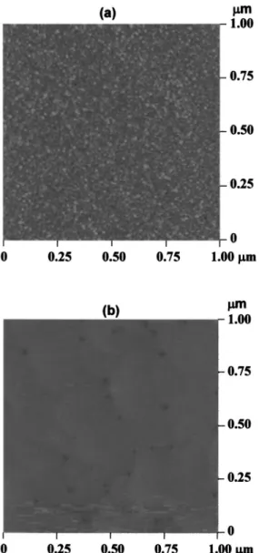
layer were also prepared for comparison 共i.e., sample B兲. One would like to note that samples used in this study were designed to have film thickness of 1.6µm which is less than the conventional SBDs having film thickness of around 4 µm. This design is purposely to manifest the effect of TDs on the electrical properties of GaN SBDs, and the LTG GaN cap layer was used to mitigate the influence resulting from TD-related surface defects. As shown in Fig. 1, one can clearly see that the TD density in the vicinity of GaN/sapphire in-terface is very high共109–1010/ cm2兲. However, the TD den-sity becomes lower as the film thickness increased. In other words, the low TD density region is far from the GaN/ sapphire interface. In addition, AFM topographic images were also used to inspect the surface morphology of the 1.6-µm-thick GaN film grown on sapphire. As shown in Fig. 2, AFM images clearly show that growth steps and dense pits can be observed in sample B without the LTG GaN cap layer 关Fig. 2共b兲兴. These pits are generally thought to be the surface termination of TDs containing electronic states near the va-lence band16and be one of the leakage sources in GaN based SBDs. In addition, the TD-induced surface pits show an in-a兲
Electronic mail: [email protected]
APPLIED PHYSICS LETTERS 86, 052103共2005兲
0003-6951/2005/86共5兲/052103/3/$22.50 86, 052103-1 © 2005 American Institute of Physics
homogeneously spatial distribution. In contrast, surface pits are almost invisible in sample A, as shown in Fig. 2共a兲. Therefore, one suggests that the LTG GaN can significantly block the surface pits and may passivate the surface defects. To understand the effect of LTG GaN layer on the reduction of leakage current, we fabricated two kinds of GaN SBDs 共i.e., sample A and sample B兲 to evaluate their current– voltage共I–V兲 characteristics. For device processing, a mesa dry etching17 was performed and then followed by a deposi-tion of Ti/Al on exposed n+-GaN as Ohmic contact, and a bilayer metal of Ni/Au 共3nm/10 nm兲 was deposited on the LTG GaN as Schottky metal.18Finally, a deposition of Ti/Au 共50 nm/1 µm兲 on the Ti/Al and the Ni/Au to serve as the bonding pad. The diameter of the fabricated circular SBDs was kept at 500µm. Room-temperature共RT兲 I–V character-istics of the fabricated SBDs were then measured by an HP4156 semiconductor parameter analyzer.
Figure 3 shows the typical RT I–V curves of the GaN SBDs共i.e., sample A and sample B兲. Under reverse bias, it was found that the leakage current was near a constant of below 1⫻10−11A for sample A. In addition, the several
dif-ferent SBD devices distributed over the wafer were measured at the same condition showing almost the same I–V curves. In contrast, leakage currents of sample B were much larger, and increased rapidly as the reverse bias increased up to a threshold voltage having an inhomogeneously spatial distri-bution. A difference in the leakage current of five orders of magnitude was obtained as reverse bias was higher than⫺5 V. This could be attributed to two possible reasons. One is that the LTG GaN layer disposed between Ni/Au and
i-GaN could result in a thicker and higher potential barrier,
as compared to conventional Schottky barrier diodes 共i.e., sample B兲. Considering the uniform distribution in leakage current of sample A, it is possible that the highly resistive LTG GaN cap layer can block most of the leakage paths caused by TD surface terminations.19 Returning to Fig. 2, one can see that the pits distributing over the GaN surface of sample B are not uniform while sample A shows a nearly featureless surface morphology. This is consistent with the
I–V characteristics in sample A having homogeneously
spa-tial distribution, as shown in Fig. 3, if the surface pits are the leakage paths of the reverse current. In general, the mecha-nisms responsible for leakage current in typical SBDs in-FIG. 1. TEM image of a typical 4-µm-thick GaN film on sapphire substrate
grown by OMVPE.
FIG. 2. Typical AFM images of sample A共a兲 and sample B 共b兲.
FIG. 3. Typical room-temperature I–V curves of sample A共a兲 and sample B
共b兲.
052103-2 Sheu, Lee, and Lai Appl. Phys. Lett. 86, 052103共2005兲
clude thermionic emission over the Schottky barrier, field-emission tunneling, and trap-assisted tunneling through the Schottky barrier. For GaN SBDs, the first one can be nearly neglected due to the large barrier height共BH兲. For the sec-ond one associated with tunneling from metal into semicon-ductor is dominant at low temperature共T⬍300 K兲. Return-ing to Fig. 3, sample B showed an abrupt increase of leakage current as the reverse biases are above the threshold values exhibiting an inhomogeneously spatial distribution. This phenomenon could be ascribed to that carrier transports are dominated by field-emission tunneling and/or trap-assisted tunneling through the Schottky barrier. Under room tempera-ture, the latter case is most likely due to electrons in the metal can be thermally activated to a trap level at the metal/ semiconductor interface and then tunnel into the semicon-ductor. As mentioned above, one expects that the trap level should be related to the TDs in the GaN film. Considering the depth of TD-related trap states, Brazel et al. suggested that there are metastable acceptor-and donor-like states coex-isting in the vicinity of dislocations and responsible for the locally high reverse leakage current in GaN SBDs.19 How-ever, Hierro et al. reported that TDs-related trap states with energy levels at 0.91 and 0.59 eV below the conduction band edge dominate the conduction mechanism of reverse leakage current in GaN SBDs.20Referring to Figs. 2 and 3, we prefer to believe that trap-assisted tunneling should be the dominant conduction mechanism for reverse leakage current in sample B. In addition, if the trap-assisted tunneling process is a rate-limiting step, the leakage current as a function of reverse biases in sample B showed an inhomogeneity in threshold voltage, as shown in Fig. 3, could be attributed to the inho-mogeneous spatial distribution of surface pits 共i.e., TD ter-minations兲, as shown in Fig. 2. For sample A, the reverse I–V curves showed a homogenous distribution and a near con-stant leakage current. Regarding to the drastic difference in spatial homogeneity of reverse I–V curves between sample A and sample B, one suggests that LTG GaN cap layer can effectively block the leakage current path caused by TD ter-minations. It should be noted that LTG GaN is very different from LTG GaAs. It is known that as-grown LTG GaAs is very conductive with carrier transport dominated by carrier hopping through deep defect bands.21,22 On the other hand, annealed LTG GaAs becomes highly resistive. Thus, an-nealed LTG GaAs is suitable to serve as the buffer layer in metal-semiconductor FETs共MESFETs兲 or as the gate insu-lator layer in metal-insuinsu-lator-semiconductor FETs 共MIS-FETs兲. In contrast, our preliminary results show that no sig-nificant difference in resistivity can be observed between the as-grown LTG GaN and the annealed LTG GaN. We would like to suggest that more detailed studies should be per-formed to inspect the annealing effects on the microscopic structures of LTG GaN.
In summary, the i-GaN/LTG–GaN/Ni/Au 共sample A兲 and the i-GaN/Ni/Au 共sample B兲 Schottky barrier SBDs were prepared by OMVPE. It was found that we could sig-nificantly reduce leakage current by introducing a LTG GaN on top of the conventional GaN SBDs. In addition, the re-verse I–V curves showed a homogeneously spatial distribu-tion and a near constant leakage current. This could be at-tributed to that the most leakage current paths, i.e., the surface termination of TDs, can be blocked by the high-resistive LTG GaN layer.
The authors would like to thank the National Science Council of the Republic of China for financially supporting this research under Contract No. NSC 93-2215-E-006-036. The authors would also like to thank Professor Y. K. Su and Professor S. J. Chang for their invaluable assistance.
1
M. E. Levinshtein, S. L. Rumyantsev, R. Gaska, J. W. Wang, and M. S. Shur, Appl. Phys. Lett. 73, 1089共1998兲.
2
X. A. Cao, S. J. Pearton, G. Dang, A. P. Zhang, F. Ren, and J. M. Van Hove, Appl. Phys. Lett. 75, 4130共1999兲.
3
Q. Z. Liu, L. S. Yu, S. S. Lau, J. M. Redwing, N. R. Perkins, and T. F. Kuech, Appl. Phys. Lett. 70, 1275共1997兲.
4
L. Wang, M. I. Nathan, T.-H. Lim, M. A. Khan, and Q. Chen, Appl. Phys. Lett. 68, 1267共1996兲.
5
C. T. Lee, Y. J. Lin, and D. S. Liu, Appl. Phys. Lett. 79, 2573共2001兲.
6
J. K. Kim, H. W. Jang, C. M. Jeon, and J.-L. Lee, Appl. Phys. Lett. 81, 4655共2002兲.
7
J. K. Sheu, Y. K. Su, G. C. Chi, M. J. Jou, and C. M. Chang, Appl. Phys. Lett. 72, 3317共1998兲.
8
P. Kozodoy, J. P. Ibbetson, H. Marchand, P. T. Fini, S. Keller, J. S. Speck, S. P. DenBaars, and U. K. Mishra, Appl. Phys. Lett. 73, 975共1998兲.
9
E. J. Miller, X. Z. Dang, and E. T. Yu, J. Appl. Phys. 88, 5951共2000兲.
10
F. Zhang, D. C. Reynolds, and D. C. Look, J. Electron. Mater. 29, 448
共2000兲. 11
D. V. Kuksenkov, H. Temkin, A. Osinsky, R. Gaska, and M. A. Khan, Appl. Phys. Lett. 72, 1365共1998兲.
12
J. C. Carrano, T. Li, P. A. Grudowski, C. J. Eiting, R. D. Dupuis, and J. C. Campbell, J. Appl. Phys. 83, 6148共1998兲.
13
E. J. Miller, D. M. Schaadt, E. T. Yu, C. Poblenz, C. Elsass, and J. S. Speck, J. Appl. Phys. 91, 9821共2002兲.
14
L. W. Yin, Y. Hwang, J. H. Lee, R. M. Kolabas, R. J. Trew, and U. K. Mishra, IEEE Electron Device Lett. 11, 561 共1990兲, and references therein.
15
J. K. Sheu, C. J. Kao, M. L. Lee, W. C. Lai, L. S. Yeh, G. C. Chi, S. J. Chang, Y. K. Su, and J. M. Tsai, J. Electron. Mater. 32, 400共2003兲.
16
P. J. Hansen, Y. E. Strausser, A. N. Erickson, E. J. Tarsa, P. Kozodoy, E. G. Brazel, J. P. Ibbetson, U. Mishra, V. Narayanamurti, S. P. DenBaars, and J. S. Speck, Appl. Phys. Lett. 72, 2247共1998兲.
17
J. K. Sheu, Y. K. Su, G. C. Chi, M. J. Jou, C. M. Chang, C. C. Liu, and W. C. Hung, J. Appl. Phys. 85, 1970共1999兲.
18
J. K. Sheu, Y. K. Su, G. C. Chi, M. J. Jou, C. M. Chang, C. C. Liu, W. C. Hung, J. S. Bow, and Y. C. Yu, J. Vac. Sci. Technol. B 18, 729共2000兲.
19
E. G. Brazel, M. A. Chin, and V. Narayanamurti, Appl. Phys. Lett. 74, 2367共1999兲
20
A. Hierro, D. Kwon, S. A. Ringela, M. Hansen, J. S. Speck, U. K. Mishra, and S. P. DenBarrs, Appl. Phys. Lett. 76, 3064共2000兲.
21
L.-W. Yin, J. P. Ibbetson, M. M. Hashemi, A. C. Gossard, U. K. Mishra, Y. Hwang, T. Zhang, and R. M. Kolbas, Appl. Phys. Lett. 60, 2005共1992兲.
22
M. Lampert and P. Mark, Current Injection in Solids共Academic, New York, 1970兲.
052103-3 Sheu, Lee, and Lai Appl. Phys. Lett. 86, 052103共2005兲