行政院國家科學委員會專題研究計畫 期中進度報告
新穎光電半導體材料,低維度微細結構及其元件構造之光學 特性研究(2/3)
計畫類別: 個別型計畫
計畫編號: NSC92-2215-E-011-001-
執行期間: 92 年 08 月 01 日至 93 年 10 月 31 日 執行單位: 國立臺灣科技大學電子工程系
計畫主持人: 黃鶯聲
計畫參與人員: 陳自雄,黃鵬仁,許宏彬,陳佳甄,陳輝勝
報告類型: 精簡報告
處理方式: 本計畫可公開查詢
中 華 民 國 93 年 6 月 8 日
I
行政院國家科學委員會補助專題研究計畫 □ 成 果 報 告
■ 期中進度報告
新穎光電半導體材料,低維度微細結構及其元件構造 之光學特性研究(2/3)
Optical Properties Study of Novel optoelectronic Semiconductor Materials, Low Dimensional Microstructures and Device Structures
計 畫 類 別 : ■ 個 別 型 計 畫 □ 整 合 型 計 畫 計 畫 編 號 : NSC 92 - 2215 - E - 011 - 001 執行期間: 92 年 8 月 1 日 至 93 年 7 月 31 日
計 畫 主 持 人 : 黃 鶯 聲
計畫參與人員:陳自雄、黃鵬仁
國立台灣科技大學電子工程所博士班研究生 許宏彬、陳輝勝、陳佳甄
國立台灣科技大學電子工程所碩士班研究生
成果報告類型(依經費核定清單規定繳交):■精簡報告 □完整報告
本成果報告包括以下應繳交之附件:
□赴國外出差或研習心得報告一份
□出席國際學術會議心得報告及發表之論文各一份
處理方式:除產學合作研究計畫、提升產業技術及人才培育研究計畫、列管計畫 及下列情形者外,得立即公開查詢
□涉及專利或其他智慧財產權,□一年□二年後可公開查詢
執行單位:國立台灣科技大學電子工程所
中 華 民 國 93 年 6 月 10 日
II
行政院國家科學委員會專題研究計畫期中精簡報告
新穎光電半導體材料,低維度微細結構及其元件構造之光學特性研究(2/3)
Optical Properties Study of Novel optoelectronic Semiconductor Materials, Low Dimensional Microstructures and Device Structures
計劃編號:NSC92-2115-E-011-001 執行期限:92 年 8 月 1 日至 93 年 7 月 31 日 主持人:黃鶯聲 國立台灣科技大學電子工程系
計畫參與人員:陳自雄、黃鵬仁、許宏彬、
陳輝勝、陳佳甄
一、中文摘要
本計畫目的主要利用非接觸式電場調 制(Contactless Electroreflectance, CER)及壓 電調制(Pizeoreflectance, PzR)反射光譜來研 究 II-VI 族 寬 能 隙 半 導 體 化 合 物 材 料 ZnCd BeS e 及 III-V 族含氮四 元化合 物 半 導 體 GaInNP 。在 ZnCdBeSe 方面,
CER 及 PzR 光譜可得到因晶格常數不匹配 所造成價電帶分裂之輕電洞(light-hole, lh) 及重電洞(heavy-hole, hh)躍遷訊號, 藉 由 PzR 光 譜 可 將 lh 分 辨 出 來 。 另 外 在 Ga In NP 部份 ,主要 使用 PzR 光譜配 合 極化 量 測 技巧 來 判 定 材料 之 非 對稱 性。
並探 討 上 述化 合 物 半 導體 不 同 訊號 隨溫 度變化之情形。
關鍵詞:非接觸式電場調制、壓電調制、
II-V I 族寬能隙半導體、氮、III-V 族四 元化合物。
Abstract
Using contactless electroreflectance and piezo-reflectance spectroscopy to characterize II-V I wide band gap material ZnCdNeSe and III-V N-rel ated quat ernar y GaIn NP films . Fro m CER an d PzR spect ra, we get bot h th e l h and h h t ransiti on en erg y, and th e PzR sp ect ra can identif y th e lh si gn al. We also obs erved th e ani so trop ic prop erties utilize po lariz ed pi ezorefl ect ance in Ga In NP films . Th e di fferent transitions energy with temperature
Variation are also evaluated and discussed.
Keywords : Contactless electroreflectance,
Piezoreflectance, II-V I wide band gap material, Nitrogen, III-V N-rel at ed q uat ern ar y compound semiconductor,二、計畫緣由與目的
近幾年來, II-VI 寬 能 隙 半 導 體 材 料 逐漸在光電產業上受到注意,因其發光波 長為較短波長屬藍光到紫外波段,可應用 於照明光源系統、大型全彩看板。因其實 用性所以目前有極多數的機構均在研究寬 能隙系列的材料。在含氮化合物半導體方 面,只要在化合物半導體中加入少量之氮 (N) 即 可 使 能 隙 大 幅 的 降 低 , 再 加 上 成 本 較低和其它優點使得含氮化合物材料在這 幾 年 來 受 到 相 當 大 的 注 目 , 如 氮 化 鎵 (GaN) 、 氮 砷 化 銦 鎵 (Ga InNAs) 等 材 料 皆 是。如 GaInNAs 材料被開發為應用於長 波長之光纖傳輸系統之光源,亦可作為雙 異質接面電晶體之基極材料,可有效的降 低 電 晶 體 之 導 通 電 壓 (turn on voltage) 。 在 GaInP 中 加 入 少 量 之 氮 而 形 成 之 Ga In NP 薄膜 可使 GaIn NP 與 GaAs 晶格 較為匹配,並且用來作為異質接面電晶體 合適之射極與集極材料。因此研究上述之 新穎光電半導體材料之特性實屬重要。
III
三、研究方法及計畫成果
研究方法
1.利用非接觸式電場調制(CER)及壓電調制 (PzR)反射光譜來得到 ZnCd BeS e 材 料 之 lh 和 hh 躍遷訊號。
2.比較 CER 與 PzR 光譜來分辨出 lh 訊號。
3.藉由溫度變化量測來得到 lh 和 hh 訊號位 置及展寬參數隨溫度變化的情形。
4.利用非接觸式電場調制(CER)及壓電調制 (PzR)反射光譜來得到 Ga In NP 薄 膜 因 非 對 稱 性 所 產 生 之 訊 號 Eg, Eg+∆12 和 Eg+∆13。
5.利用不同方向偏極光的非接觸式電場調制 (CER)及壓電調制(PzR)反射光譜來觀察 GaInNP 薄膜的非對稱性。
6. 藉由溫度變化的極化壓電調制光譜來得 到 Eg, Eg+∆12 和 Eg+∆13三訊號隨溫度變 化的情形。
計畫成果:
1. C. H. Hsieh, Y. S. Huang, C. H. Ho, K. K.
Tiong, M. Munoz, O. Maksimov and M. C.
Tamargo, “Temperature Dependence of the Band-Edge Transitions of ZnCdBeSe”, J.
Jpn. Appl. Phys., Vol. 43, pp. 459-466
(2004).2. H. P. Hsu, Y. S. Huang, C. W. Wu, Y. K.
Su, F. S. Juang, Y. G. Hong and C. W. Tu,
“The Structural and Optical Characterization of a New Class of Dilute Nitride Compound Semiconductors:
GaInNP”, J. Phys. Condens. Matter, be published in July (2004)
3. Y. K. Su, C. W. Wu, S. H. Hsu, S. J. Chang, W. C. Chen, Y. S. Huang, and H. P. Hsu,
“Observation of Spontaneous ordering in the optoelectronic material GaInNP”, Appl.
Phys. Lett. Vol. 84, pp. 1299-1301 (2004).
4. Y. K. Su, C. H. Wu, Y. S. Huang, H. P. Hsu, W. C. Chen, S. H. Hsu and S. J. Chang,
“Piezoreflectance and Contactless Electroreflectance Spectra of an Optoelectronic Material: GaInNP Grown on GaAs substrates”, J. Crystal. Growth, Vol.
264, pp. 357-362 (2004).
四、結果與討論
利用 CER 和 PzR 技巧量測不同 Be 含量之 ZnCdBeSe 薄膜可正確地得到 lh 和 hh 的訊 號,在溫度變化(15K-450K)的量測中,發現加 入 Be 後使能隙隨溫度變化的程度趨緩,並且 求出 lh 和 hh 躍遷訊號的能隙位置和展寬參 數,和其它相類似之材料比較。另一方面,利 用極化的 PzR 光譜可觀察出一系列氮含量不同 的 GaInNP 薄膜的非對稱性質,證明在 GaInP 中加入 N 仍有著非對稱性質,並正確地得到 價帶分裂的 Eg, Eg+∆12 和 Eg+∆13訊號。再藉由 溫度變化求出價帶分裂之三訊號之溫度參數,
並與其它含氮化合物材料作一比較,發現在低 溫區域(15K-300K)中,其溫度參數並無因加入 氮後有太大的變化。從以上結果中,皆能有效 且深入地加以探討新穎光電半導體材料之特 性。。
五、參考文獻
1. L. Malikova, W. Krystek, F. H. Pollak, N.
Dai, A. Cavus and M. C. Tamargo, Phys..
Rev. B, 54 (1996) 1819.
2. F. Fisher, G. Landwehr, Th. Litz, H. J.
Lugauer, U. Zehnder, Th. Gerhard, W. Ossau and A. Wang, J. Crystal Growth, 175/176 (1997) 552.
3. Y. G. Hong, R. Andre and C. W. Tu, J. Vac.
Sci. Technol. B, 19 (2001) 1413.
4. H. P. Xin, R. J. Welty, Y. G. Yong, and C.
W. Tu, J. Crystal Growth, 227/228 (2001) 558.
5. Y. G. Hong, F. S. Juang, M. H. Kim and C.
W. Tu, J. Crystal Growth, 251 (2003) 437.
IV Figure 1. CER and PzR spectra for three different compositions of ZnCdBeSe samples in spectral range between 1.9 and 2.4 eV at (a) 15 K and (b) 300 K.
Figure 2. The temperature variations of light-hole (lh) and heavy-hole (hh) transition energies of (a) Zn0.38Cd0.62Se (Sample A), (b) (Zn0.38Cd0.62)0.93Be0.07Se (Sample B), and (c) (Zn0.38Cd0.62)0.89Be0.11Se (Sample C) with representative error bars. The solid curves are least-squares fits to the Varshni-type semiempirical relationship and the dashed lines are fitted to the Bose-Einstein-type expression.
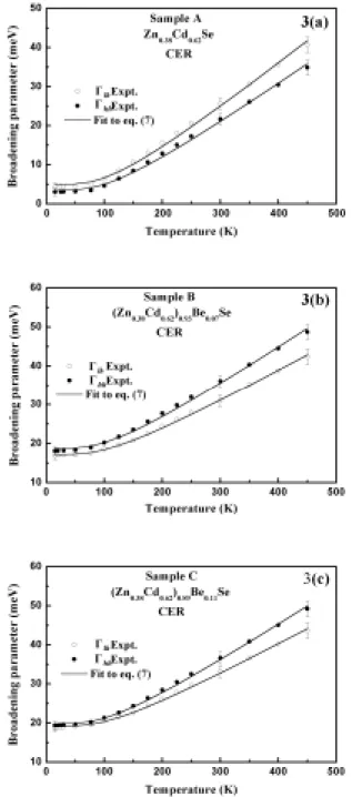
Figure 3. Experimental variation of the broadening parameter (HWHM) for the direct excitonic transitions of (a) Zn0.38Cd0.62Se (Sample A), (b) (Zn0.38Cd0.62)0.93Be0.07Se (Sample B), and (c) (Zn0.38Cd0.62)0.89Be0.11Se (Sample C) with representative error bars. The open and solid circles are respectively the experimental values of lh and hh transitions, respectively, and the solid lines are least-square fits to eq. (7).
V Figure 4. Room temperature polarized CER and PzR spectra of Ga0.46In0.54NxP1-x epilayers with nitrogen content x = 0, 0.5% and 1% in the vicinity of band edge. The energies of near band edge critical points transitions Eg, Eg+∆12 and Eg+∆13 obtained from the fits are indicated by arrows.
Figure 5. PzR spectra for E || [110] of Ga0.46In0.54N0.01P0.99 (Sample C) at several temperatures between 15 and 300 K. The dashed lines are the experimental curves and the solid lines are least- squares fits to Lorentzian line shape.
Figure 6. PzR spectra for E ||
[ 1 1 0 ]
of Ga0.46In0.54N0.01P0.99 (Sample C) at several temperatures between 15 and 300 K.The dashed lines are the experimental curves and the solid lines are least-squares fits to Lorentzian line shape.
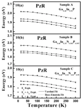
Fig 7. The temperature variations of Eg, Eg+∆12 and Eg+∆13
for (a) Ga0.46In0.54P (Sample A), (b) Ga0.46In0.54N0.005P0.995 (Sample B), and (c) Ga0.46In0.54N0.01P0.99 (Sample C) with representative error bars. The solid curves are least-squares fits to the Varshni-type semiempirical relationship and the dotted lines are fitted to the Bose-Einstein-type expression.