行政院國家科學委員會專題研究計畫 成果報告
電感在毫微米金氧半電晶體上三維構造的元件與電路應用 性的研究
研究成果報告(精簡版)
計 畫 類 別 : 個別型
計 畫 編 號 : NSC 95-2221-E-011-173-
執 行 期 間 : 95 年 08 月 01 日至 96 年 07 月 31 日 執 行 單 位 : 國立臺灣科技大學電子工程系
計 畫 主 持 人 : 張勝良
計畫參與人員: 博士班研究生-兼任助理:李少華、李建鋒、莊昀學、劉政辰
報 告 附 件 : 出席國際會議研究心得報告及發表論文
處 理 方 式 : 本計畫可公開查詢
中 華 民 國 96 年 07 月 13 日
行政院國家科學委員會補助專題研究計畫 行政院國家科學委員會補助專題研究計畫 行政院國家科學委員會補助專題研究計畫
行政院國家科學委員會補助專題研究計畫 ████ 成 果 報 告成 果 報 告成 果 報 告成 果 報 告
□
□
□
□期中進度報告期中進度報告期中進度報告期中進度報告
電感在毫微米金氧半電晶體上三維構造的元件與電路應用性的研究
計畫類別:
█
個別型計畫 □ 整合型計畫 計畫編號:NSC 95-2221-E-011-173-
執行期間:
95
年08
月01
日 至96 年 07 月 31 日
計畫主持人:張勝良
共同主持人:
計畫參與人員:
李少華、李建鋒、莊昀學、劉政辰
成果報告類型(依經費核定清單規定繳交):
█
精簡報告 □完整報告本成果報告包括以下應繳交之附件:
□赴國外出差或研習心得報告一份
□赴大陸地區出差或研習心得報告一份
█出席國際學術會議心得報告及發表之論文各一份
□國際合作研究計畫國外研究報告書一份
處理方式:除產學合作研究計畫、提升產業技術及人才培育研究計畫、列管計 畫及下列情形者外,得立即公開查詢
□涉及專利或其他智慧財產權,█一年□二年後可公開查詢
執行單位:
國立台灣科技大學電子工程系
中 華 民 國 96 年 07 月 06 日
電感在毫微米金氧半電晶體上三維構造的元件與電路應用性的研究
“STUDY ON THE DEVICE AND CIRCUIT APPLICATION OF THE INDUCTOR OVER NANOMETER MOSFET 3-DIMENSIONAL STRUCTURE”
計畫編號:
NSC 95-2221-E-011 -173 -
執行期間:96 年 08 月 01 日 至 96 年 07 月 31 日 主持人:張勝良 國立台灣科技大學電子工程系教授
一、 中文摘要
本報告使用 0.18-um 1P6M CMOS 製程,設 計製作一個三維(3-D)電感除頻器。本除頻器組 合兩個單端互補式考畢茲振盪器,並且使用電 容耦合產生差動輸出信號。使用三維電感的目 的在減少晶片的面積。本除 2 的 LC 共振腔注 入鎖定除頻器的完成,需要加入注入 nMOS 在除頻器輸出的兩端。
量測結果驗證了在供應電壓 1.6 V 時,除頻 器的自然振盪頻率可調範圍為 3.05 GHz 到 3.52 GHz,以及當注入信號功率為 0 dBm,注 入信號頻率為 5.3 GHz~8.2 GHz 時,鎖定範圍 為 2.9 GHz (43%)。
核心電路的功率消耗為7.14 mW,晶片面積 為0.625 x 0.672 mm2 。
關鍵詞: CMOS,考畢茲振盪器,注入鎖定除 頻器,鎖定範圍,三維(3-D)電感。
英文摘要
The design of a frequency divider (FD) employing 3-dimensional (3-D) inductors fabricated in the 0.18-um 1P6M CMOS technology is reported. The FD consists of two single-ended complementary Colpitts oscillators coupled with capacitors to generate differential output signals. The aim of using 3D inductor is to reduce chip size. The divide-by-2 LC-tank injection-locked frequency divider is performed
by adding an injection nMOS between the differential outputs of the divider. The measurement results show that at the supply voltage of 1.6V, the divider free-running frequency is tunable from 3.05 GHz to 3.52 GHz, and at the incident power of 0 dBm the locking range is about 2.9 GHz (43%), from the incident frequency 5.3 GHz to 8.2 GHz. The core power consumption is 7.14mW. The die area is 0.625 x 0.672 mm2.
Keywords: CMOS, Colpitts oscillator, inject- tion-locked frequency divider, locking range, 3-dimensional inductor.
I. INTRODUCTION
Frequency divider (FD) is widely used in h i g h - s p e e d s ys t e m s s u c h a s f r e q u e n cy synthesizers and used for quadrature signal generation. The main concern for the frequency divider design is lower power consumption, wide locking range, high frequency capability, and low cost. High frequency dividers can be realized using common-mode logic (CML), dynamic logic, and Miller divider, or through the injection locked oscillators (ILO). Injection locked oscillators consume generally less power than CML or Miller dividers due to the tuned nature of the circuit, they are widely used to divide down high oscillation frequency [1,2,3,4]. The
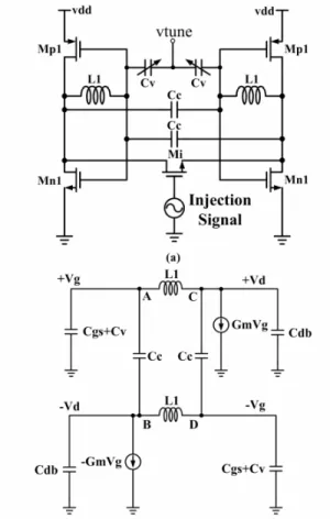
Fig. 1. (a) Schematic of the proposed VCO with two Colpitts VCO cores. (b) Small-signal equivalent circuit without injection nMOS.
conventional injection locked oscillator has two injection methods, one is based on the current source injection and the other is based on the direct injection. The former is not a good choice for high frequency operation due to the existence of large parasitic capacitance at the drain node of the tail. The popular LC tank based injection l o c k e d f r e q u e n c y d i v i d e r ( ILF D ) u s e s cross-coupled MOS switching pairs with easy implementation. Other LC tank based ILFDs are rarely studied.
In this paper, we propose a new differential ILFD, which is composed of two single-ended complementary Colpitts oscillators [5] embedded with an injection MOSFET. The two Colpitts oscillators are coupled with capacitors in order to
Fig. 2. The simulated relationship between ac input voltage and ac output voltages of the differential ILFD. Solid line: injection signal.
Circled and cross lines: two drain outputs.
generate balanced outputs. Because of the coupling capacitors, the operation principle of this ILFD is based on the series tuned LC resonator rather than the parallel tuned LC resonator. The latter is the most popular LC resonator due to easy understanding and implementation. The oscillator based on parallel tuned LC tank can be Colpitts oscillator [6], Hartley oscillator [7], or cross-coupled oscillator.
The series tuned oscillator is often referred to as Clapp oscillator [8]. Therefore the proposed CMOS circuit becomes a Clapp oscillator based ILFD. In order to reduce the chip area, two symmetric 3 dimensional inductors in the chip implementation are adopted. MOS varactors are used to extend the locking range of the proposed ILFD.
II. CIRCUIT DESIGN
There are many ways to make a differential VCO uses the single-ended Colpitts VCO[5].
Fig. 1(a) shows the proposed differential ILFD circuit. There are two single-ended Colpitts oscillators (composed of Mp1, Mn1 and L1) combined into one differential circuit. The two single-ended complementary Colpitts oscillators
are coupled by two capacitors Cc, which force the two oscillators operate in a differential form.
Fig. 1(b) shows the small-signal equivalent circuit without injection nMOS. In Fig. 1(b), gm
(=gmp+ gmn) is the net transconductance due to the transistors Mn1 and Mp1. Cgs(=Cgsn+Cgsp) is the net gate-source capacitance due to the transistors Mn1 and Mp1. Cdb (=Cdsp +Cdsn) is the net capacitance seen at the drain node of the transistors Mn1 and Mp1. Cv is the varactor capacitance. Mi is omitted in Fig. 1(b).
Neglecting the current sources, applying Kirchhoff’s current law at nodes A and B in Fig.
1(b) yields:
1
] [
]
[ sL
V V V
V sC V C C
s gs v g c g d d g
−
= + +
+ (1)
1
]
[ sL
V V V
V sC V
sCdb d c g d g d
+
−
= +
−
− (2)
Using Eqs. (1) and (2) yields the radian oscillation frequency
])]
([
]) ([
[
4 )
(
1 db gs v db c c gs v
c db v gs
C C C C C C C C L
C C C C
+ +
+ +
+ + + ω=
(3)
The above equation indicates that we can change the capacitance value of the varactor by applying a tuning voltage to set the free-running oscillation frequency. The circuit shown in Fig.
1(b) can be decomposed into two series tuned LC tanks connected in parallel with back to front by bi-setting the whole circuit into two half circuits along the nodes A and D. The differential VCO is composed of two single-ended Colpitts oscillators with two independent dc current paths. However, the operation principle is different from differential Colpitts oscillator, the LC resonator is a series-tuned rather than parallel-tuned. In the small-signal circuit model shown in Fig. 1(b), we
Fig. 3. 3D view of the used inductor.
intentionally neglect the presence of dissipation parasitic resistor for simplicity, the loss due to the parasitic resistors is compensated by the voltage controlled current sources. When the coupling capacitance Cc is too small, the two Colpitts oscillators operate independently. As the Cc increases and is small, its role is to force the two single-ended Colpitts oscillators to operate in differential mode. When the effective coupling capacitance Cc is very large, the ac function of the circuit approximates that of a complementary cross-coupled LC tank oscillator, however the dc current paths of the proposed VCO and cross-coupled VCO are different.
In Fig. 1(a), the drain and source of the injector MOS Mi are connected to the output nodes of the divider. The dc bias of injection MOS and its parasitic components can affect the frequency tuning curve. The injection mechanism is basically a direct injection technique proposed in [1]. The relationship between the ac injection signal and the ac outputs of ILFD is shown in Fig. 2. Under injection locked condition, the voltages at the two outputs are equalized at the maximum injection signal strength. Between the two peak injection signal voltages, there is one peak output voltage at the drain outputs, which thus oscillate by half of the injection cycles. Since the drain outputs of the transistor are forced to operate differentially by the coupling capacitor Cc, the
Fig. 4. Micro-photo of the fabricated ILFD.
divider’s drain outputs are differential.
Fig. 3 shows a 3-D view of the designed in du cto r usi n g 5 top metal layers. The multi-layer inductor structure consists of planar spiral inductors laid out on different metal layers-one overlapping the other. The spirals in the fully symmetric 3D inductor [9] wind in and down alternately after every half run. The location of the two ports on the same side of the spiral can be an advantage in circuit layout.
The inductor design was carried out using the Agilent ADS Momentum EM simulator. A large inductance value can be achieved in small area by using more metal layers in the 3D inductors.
However, this is at the cost of reduced Q due to thinner metal layers used and the higher number of poor conducting vias. Q-factor optimization of passive inductor and capacitor is important in the ILFD design. Lower Q results in more power consumption in ILFD and larger locking range.
III. MEASUREMENT AND DISCUSSION
The proposed circuit has been implemented in a standard triple-well 0.18-um 1p6M CMOS technology. Fig. 4 shows the photo of the fabricated chip. The chip area is 0.625 x0.672 mm2 including pads. Two 3-D inductors are shown. The measured tuning range of the free running ILFD is shown in Fig. 5. The tuning range of FD is from 3.05 GHz to 3.52 GHz at
Fig. 5. Measured output frequency versus control voltage. Vdd= 1.6V
Fig. 6. Measured input sensitivity of the ILFD with 2 division ratio.
Fig. 7. Measured phase noises of the reference injection source and the divider output in
2
÷ mode.
Vdd=1.6 V. The varactors are accumulation mode nMOS varactors, as the gate voltage of the varactors (i.e., Vtune) increases, the varactor’s capacitance decreases, therefore the oscillation frequency increases. Fig. 6 shows the measured relationship between input sensitivity and operating frequency of the frequency divider with 2 division ratio under the condition of Vtune
Fig. 8. Measured output spectra of the divider before and after locking.
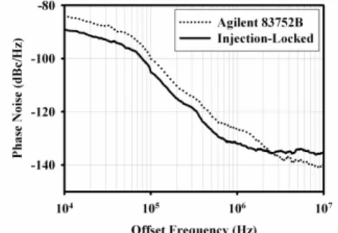
= 0.0, 0.8 and 1.6 V and Vdd = 1.6 V, with a total locking range from 5.3 to 8.2 GHz. The dc bias Vinj of injector’s gate is 1.1V. The current and power consumption of the core are 4.49 mA and 7.14 mW respectively. Fig. 7 shows the measured phase noises of the injection signal and the injection-locked oscillator output in the ÷2
mode. The phase noise of the injection-reference is -125 dBc/Hz at 1-MHz offset. After applying an external power injection at -3 dBm, the output ILFD phase noise is about -134 dBc/Hz in the
2
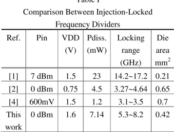
÷ mode. The phase noise of free-running ILFD at 1MHz offset from the output oscillation frequency of 3.2 GHz is about -100 dBc/Hz. The phase noise of ÷2 ILFD is lower than that of the free-running oscillator by 34 dB. Fig. 8 shows the measured output spectra of the divider before and after the locked conditions in the ÷2 mode. The locked output spectrum is sharper and shows a lower phase noise. Table I shows the comparison between the proposed injection- locked divider and previously published reports.
IV. CONCLUSION
A new divide-by-2 frequency divider circuit has been proposed and implemented in the 0.18-um CMOS technology. The differential Clapp injection locked frequency divider uses
Table I
Comparison Between Injection-Locked Frequency Dividers
Ref. Pin VDD (V)
Pdiss.
(mW)
Locking range (GHz)
Die area mm2 [1] 7 dBm 1.5 23 14.2~17.2 0.21 [2] 0 dBm 0.75 4.5 3.27~4.64 0.65 [4] 600mV 1.5 1.2 3.1~3.5 0.7 This
work
0 dBm 1.6 7.14 5.3~8.2 0.42
symmetric 3D inductors to save die area. The die area is 0.625 x0.672 mm2. The implemented FD core consumes power of 7.14 mW at 1.6 V supply voltage, and the measured locked phase noise is -134 dBc/Hz at 1-MHz offset from the output oscillation frequency of 3.2 GHz. At the incident power of 0 dBm the locking range is from 5.3 GHz to 8.2 GHz.
REFERENCES
[1] M. Tiebout, “A CMOS direct injection- locked oscillator topology as high-frequency low-power frequency divider,” IEEE J.
Solid-State Circuits, vol. 39, pp. 1170 – 1174, July 2004.
[2] Y.-H. Chuang, S.-H. Lee, R.-H. Yen, S.-L.
Jang, J.-F. Lee and M.-H. Juang,” A wide locking range and low voltage CMOS direct injection-locked frequency divider,” IEEE Microw. Wireless Compon. Lett., vol. 16, no.
5, pp. 299-301, May 2006.
[3] J. Lee and B. Razavi, “A 40GHz frequency divider in 0.18-um CMOS technology,” in VLSI Circuits Tech. Dig., pp.259-262, June 2003.
[4] H. R. Rategh and T. H. Lee, “Superharmonic injection-locked frequency dividers,” IEEE J.
Solid-State Circuits, vol. 34, pp. 813–821, June 1999.
[5] C.- Y. Cha and S.-G. Lee,"A complementary Colpitts oscillator based on 0.35 um CMOS technology," IEEE ESSCIRC, pp. 691-694, Sep. 2003.
[6] R. Aparicio and A. Hajimiri, "A noise- shifting differential Colpitts VCO," IEEE J Solid-State Circuits, vol. 37, pp. 1728-1736, Dec. (v) 2002.
[7] S.-H. Lee, Y.-H. Chuang, S.-L. Jang and C.-C. Chen, ” Low-phase noise Hartley differential CMOS voltage controlled oscillator,” IEEE Microw. Wireless Compon. Lett., pp. 145-147, Feb. 2007.
[8] S. Shekhar, S. Aniruddhan, and D. J.
Allstot,” A fully-differential CMOS Clapp VCO for IEEE 802.1la applications,” IEEE Intl. Symposium on Circuits and Systems, pp.3241-3244, 2006.
[9] W.-Z. Chen and W.-H. Chen、”Symmetric 3D passive components for RF ICs application,” IEEE MTT-S Int. Microw.
Symp. Dig., pp. A85- A88, 2003.
計畫成果自評部份
本計畫對於學術研究、配合國家通訊科技發展及其他應用方面預期之貢獻包括了:
1. 本計畫在研究毫微米互補式金氧半場效電晶體電路的特性,並且使用三維整合電感和主動金氧 半場效電晶體來設計達到節省晶片面積,同時保有良好的電路與元件性能。
2. 最終完成 Injection Locked Frequency Divider (ILFD)整體的 IC layout、IC 下線生產程序以及晶 片量測工作,因此應可培養研究生及老師 RF CMOS 系統電路設計及實作的能力,讓學校的研 究工作與無線通訊產業界所需的發展方向一致,藉以達成國家通訊科技發展的目標。
可供推廣之研發成果資料表
█ 可申請專利 █ 可技術移轉 日期:96 年 07 月 06 日
國科會補助計畫 國科會補助計畫 國科會補助計畫 國科會補助計畫
計畫名稱:電感在毫微米金氧半電晶體上三維構造的元件與電路應 用性的研究
計畫主持人:張勝良
計畫編號:
NSC 95-2221-E-011-173-
學門領域:固態電子技術 技術 技術
技術/ // /創作名稱 創作名稱 創作名稱 創作名稱
電感在毫微米金氧半電晶體上三維構造的元件與電路應用性的研 究/
電感在毫微米金氧半電晶體上三維構造的元件與電路應用性的研 究
發明人 發明人 發明人
發明人/ // /創作人 創作人 創作人 創作人
張勝良/張勝良中文:
本報告使用 0.18-um 1P6M CMOS 製程,設計製作一個三維(3-D) 電感除頻器。本除頻器組合兩個單端互補式考畢茲振盪器,並且使 用電容耦合產生差動輸出信號。使用三維電感的目的在減少晶片的 面積。本除 2 的 LC 共振腔注入鎖定除頻器的完成,需要加入注入 nMOS 在除頻器輸出的兩端,
量測結果驗證了在供應電壓 1.6 V 時,除頻器的自然振盪頻率可 調範圍為 3.05 GHz 到 3.52 GHz,以及當注入信號功率為 0 dBm,
注入信號頻率為 5.3 GHz~8.2 GHz 時,鎖定範圍為 2.9 GHz (43%)。
核心電路的功率消耗為7.14 mW,晶片面積為0.625 x 0.672 mm2 。
技術說明 技術說明 技術說明 技術說明
英文:
The design of a frequency divider (FD) employing 3-dimensional (3-D) inductors fabricated in the 0.18-um 1P6M CMOS technology is reported. The FD consists of two single-ended complementary Colpitts oscillators coupled with capacitors to generate differential output signals. The aim of using 3D inductor is to reduce chip size. The divide-by-2 LC-tank injection-locked frequency divider is performed by adding an injection nMOS between the differential outputs of the divider.
The measurement results show that at the supply voltage of 1.6V, the divider free-running frequency is tunable from 3.05 GHz to 3.52 GHz, and at the incident power of 0 dBm the locking range is about 2.9 GHz (43%), from the incident frequency 5.3 GHz to 8.2 GHz. The core power consumption is 7.14mW. The die area is 0.625 x 0.672 mm2.
可利用之產業 可利用之產業 可利用之產業 可利用之產業
及 及 及 及 可開發之產品 可開發之產品 可開發之產品 可開發之產品
1. For Wireless Systems 2. For High Speed Data Links
技術特點 技術特點 技術特點 技術特點
1. Low Phase Noise ( -134 dBc/Hz @ 1MHz ) 2. Wider Locking range ( 5.3 GHz ~ 8.2 GHz ) 3. Small Chip Area ( 0.625 * 0.672 mm2 )
推廣及運用的價 推廣及運用的價 推廣及運用的價 推廣及運用的價
值 值 值 值
1. Low Phase Noise ( -134 dBc/Hz @ 1MHz ) 2. Wider Locking range ( 5.3 GHz ~ 8.2 GHz ) 3. Small Chip Area ( 0.625 * 0.672 mm2 )
※ 1.每項研發成果請填寫一式二份,一份隨成果報告送繳本會,一份送 貴單位研發成果 推廣單位(如技術移轉中心)。
※ 2.2.2.本2.本本本項研發成果若尚未申請專利項研發成果若尚未申請專利項研發成果若尚未申請專利項研發成果若尚未申請專利,,,,請勿揭露可申請專利之主要內容請勿揭露可申請專利之主要內容請勿揭露可申請專利之主要內容請勿揭露可申請專利之主要內容。。。。
※ 3.本表若不敷使用,請自行影印使用。
出席國際學術會議心得報告 出席國際學術會議心得報告 出席國際學術會議心得報告 出席國際學術會議心得報告
計畫編號 NSC 95-2221-E-011-173
計畫名稱 電感在毫微米金氧半電晶體上三維構造的元件與電路應用性的研究
出國人員姓名 服務機關及職稱
(中文)李建鋒 (英文)Chien-Feng Lee
國立台灣科技大學電子工程研究所博士班四年級
會議時間地點 自 2006 年 12 月 4 日至 2006 年 12 月 7 日止於新加坡舉行
會議名稱 (中文) 2006 亞洲太平洋電路與系統研討會議
(英文) APCCAS2006
發表論文題目 (中文) 低電壓 2.4 GHz 壓控振盪器使用 3D 螺旋電感
(英文) A Low-Voltage 2.4GHz VCO with 3D Helical Inductors 一、參加會議經過
第八屆 IEEE 2006 亞洲太平洋電路與系統研討會議(IEEE APCCAS 2006, the 8th of the biennial Asia Pacific Conference on Circuits and Systems)於 2006 年 12 月 4 日至 12 月 7 日於新加坡舉行。本研討會為 世界各國投入相關研究學者所必定參加的重要會議之一,今年大會審核後約五百篇於大會發表。此研討 會涵括通訊基礎研究到電路應用發展等領域,範圍相當廣泛。
本人於此次會議中發表的論文為“A Low-Voltage 2.4GHz VCO with 3D Helical Inductors”,於12月6日 上午9點,於Session:voltage-control oscillator中做口頭報告。
會中主持人及與會人士提出許多問題討論,並於會後與參加研討會學者等作意見交換,獲益匪淺。
二、與會心得
本人非常榮幸能夠在這一次的會議上台作口頭報告,這是我第一次到新加坡,當然十分緊張。最後 總算雨過天晴,雖然我只給自己的表現打 70 分,不過我想有了這次寶貴的經驗,下一次我一定能表現 的更好。而且我的報告也引起了許多與會學者們的興趣,也提出他們的問題和看法。我想這對我的研究 工作有很大的幫助,能夠出席國際會議,除了可以讓自己的研究成果公諸於世之外,也可以觀摩其它國 家學者在相關領域上的研究,當然也可以利用這樣的機會與其他學者交換研究的心得。而藉由這一次參 加國際會議的機會,讓我認識了一些大師級的人物,他們並非像我以前想像的那麼遙遠。也讓我體會到 學術是沒有國界的,唯有時常與國際交流,才不會形成「閉門造車」的現象。
以下為本次會議最主要的四個收穫:
1. 與會人員可以瞭解個人無線通訊系統相關研究、發展最新進展。
2. 與會人員可以交換經驗心得。
3. 學術界與國內外工業界可以進行交流、洽談研究工作。
4. 我國相關研究成果及建設可以讓國際人士瞭解。
A Low-Voltage 2.4GHz VCO with 3D Helical Inductors
S.-H. Lee, Y.-H. Chuang, L.-R. Chi, S.-L. Jang, and J.-F. Lee
Department of Electronic Engineering National Taiwan University of Science and Technology 43, Keelung Road, Section 4,Taipei,Taiwan 106,R.O.C.
E-mail:[email protected] Abstract—The design of a low-voltage 2.4GHz
voltage controlled oscillator (VCO) employing 3D helical inductors fabricated in the 0.18-um 1P6M CMOS technology is reported. The LC resonators consist of two 3D helical inductors and varactors.
The aim of using 3D inductor is to reduce chip size, the inductance of inductor is designed to be 2nH, and the size of the inductor is 155x155 um2. At the supply voltage of 1.0V, the VCO core consumes power of 2.6 mW and the measured phase noise is –116.8dBc/Hz at 1MHz offset from the oscillation frequency of 2.46GHz. The output frequency can be tuned from to 2.06GHz to 2.5GHz.
Index Terms
CMOS, voltage-controlled oscillator (VCO), 3D helical inductor, tuning range.
I. INTRODUCTION
Fully integrated voltage controlled oscillator (VCO) is one of the most challenging parts of radio transceiver to integrate in standard CMOS technologies, because many demanding design parameters of VCO are required, these parameters are large frequency tuning range, low power consumption, low cost and low phase noise. A wide tuning range is often important because it can accommodate more process and temperature variations. In this paper, we propose a low voltage and small chip area CMOS VCO circuit topology intended for increasing the performance of VCO. A helical inductor [2] is used because the area occupation of helical inductor is much smaller. In addition, smaller area occupation gives smaller
substrate loss, so little performance degradation of the helical inductor over the planar spiral is expected.
As the supply voltage decreases, the tuning range decreases because of smaller applied tuning voltage.
To reduce VCO power consumption and phase noise, the tank inductance should be maximized [1], and a large varactor with high Cmax/Cmin ratio for a wider frequency tuning range is required, because the frequency of oscillation
ω
0 of an LC tank VCO is determined by) (
1
0
V
FIX C
C
L +
ω = (1) where CV is the varactor capacitance and CFIX is the fixed parasitic capacitance due to the inductor layout and transistors necessary for the compensation of the loss in the resonator. As
ω
0 is specified, this forces a minimization of the total tank capacitance.In the proposed VCO circuit, we use a concept of tapped LC tank [3] for reducing the effect of the parasitic capacitances of active transistors to increase the tuning range of VCO. The following text addresses the design concept and the details of the implemented VCO.
II. DESIGN OF LOW-VOLTAGE WIDE-BAND VCO Firstly, the operation principle of a conventional singly cross-coupled LC VCO shown in Fig. 1 is reviewed. An ideal LC oscillator is composed of an inductor and a capacitor. Ideally if the tank is lossless, the oscillator has no phase noise since the tank quality is infinite. Since practical LC tanks are lossy, a means providing negative resistance is required to
sustain the oscillation. The differential pair shown in Fig. 1 gives a small signal negative differential conductance across the tuned circuit. If this overcomes the positive loss conductance of the tuned circuit, then the natural response of the circuit is a growing oscillation, eventually limited in amplitude by circuit nonlinearity. The LC tank of the VCO is made of two inductors, the parasitic capacitances of transistors (MN1 and MN2), and two varactors (CV1 and CV2). Within the VCO, the inductors and varactors, which lie at the core, set the oscillation frequency and their losses largely determine the performance of the VCO itself. This cross-coupled architecture provides accurate differential outputs. Its output frequency can be controlled by varying the control voltage Vtune between the varactors CV1 and CV2. The oscillation amplitude of the topology of Fig. 1 is well above the supply voltage (in principle, it can be twice as much). This means that the supply voltage has to be kept lower than the maximum value allowed by the technology and the oscillation amplitude must be limited to guarantee process reliability [4].
V d d
V G
M N 1 M N 2
M N 3
L L
V t u n e
C V 1 C V 2
Fig. 1. Current-biased differential LC oscillator. VG the tail bias and Vdd the supply voltage. MN3 the tail biased transistor.
Vdd
L L
Vtune
CV1 CV2
o
To differential pair
Vdd
Vtune
CV1 CV2
o
To differential pair L/2
L/2
L/2 L/2
(a) (b)
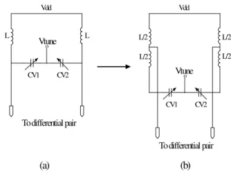
Fig. 2. (a) LC resonator (b) a tapped inductor capacitor resonator [3].
Fig. 1 shows a conventional current-biased differential LC oscillator, in which the drains and gates of cross-coupled differential pair are connected to the two terminals of the varactors in the resonator.
In this way there is no freedom to independently set the maximum gate and drain voltages. Fig. 2 shows the LC resonator transformed into a tapped resonator, an inductor L in (a) splitted into two inductors with inductance L/2 in (b) in series. The same inductor and capacitor are used in both resonators. Fig. 3 employs the tapped inductor in Fig. 2(b) to form an LC resonator. Using the tapped resonator, we can set the drain and gate voltages at different maximum value. On the one hand, the source-to-drain breakdown voltage and gate-oxide breakdown voltage are different; on the other hand, the MOS is turned on as long as the gate-source voltage Vgs is larger than the threshold voltage VT, however there is no minimum voltage limitation for the drain-to-source voltage Vds. In the proposed VCO circuit the maximum amplitude of Vgs is larger than the maximum amplitude of Vds.
o o
Vdd
Vtune
Vbias Vbias
VG
MN1 MN2
MN3 C3
L1
L2
L3
L4
C1 C2
MN4 MN5
Out +
Out
L5 L6 -
R1 R2
. .
. . .
. .
.
. .
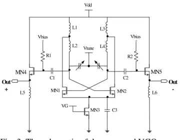
Fig. 3. The schematic of the proposed VCO.
In the VCO circuit shown in Fig. 3, the transistors MN1 and MN2 are the cross-coupled pair and provide negative resistances for the VCO core to cancel the resistive loss in the LC tank circuit. The LC tanks include varactors, and tapped inductors (L1, L2, L3, and L4), and a tail transistor (MN3). The tail MOS transistor MN3 is used to optimize the power dissipation and phase noise. The capacitor C3 is used to reduce second-harmonics and reduce tail source noise up-conversion. In order to operate the oscillator at low supply voltage and to reduce the phase noise, a large output swing of the resonant tank is needed.
The large output swing is applied to the gates of the cross-coupled transistors, so that the circuit can operate at low voltage. The large voltage swing must be limited so that no degradation in gate oxide is induced. One common drain stage is used as buffer. This buffer can directly drive the off-chip 50ohm load. The only requirement for the buffer is that it should not load the oscillator excessively.
Referring to Fig. 1, at low frequencies, the flicker noise in the switching drain currents sees a low impedance at its drain terminal [2], this impedance can be seen as a short, this will reduce the AM-PM phase noise. In the circuit shown in Fig. 3, a similar conclusion is applicable. Besides, the high frequency noise that comes from drain currents will see an inductor, which blocks the pass of the noise to
modulate the varactor, therefore the conversion of low-frequency and high-frequency drain current noise to the phase noise can be minimized.
To increase the VCO tuning range we must minimize the drain-source capacitance Cdb of switching pair by layout optimization. In addition, we can shift Cdb away from the paralleling with the varactors in LC resonator, this can be achieved using the tapped LC resonator as shown in Fig. 3, where the gates of nMOS cross-coupled transistors are connected to the terminals of the varactors, while the drain terminals of the switching MOS pairs are connected to the taps of the inductors. Simulation results indicate the tuning range increases using the tapped LC tanks.
III. HELICAL INDUCTOR DESIGN
Figure 4 shows a 3D view of a helical inductor using 4 top metal layers. The turn of the helical inductor is expanded vertically. Therefore, the 3D helical inductors have smaller occupation area compared with planar inductors. Port 1 is placed at the top metal (M6) while Port 3 is located in the bottom metal (M3) and Port 2 is designed with a tap points in the middle metal (M5) using the Agilent ADS Momentum EM simulator. The size of the inductor is 155x155 um2 and the inductance is designed to be 2nH. The tapped point is designed to
Fig. 4. 3D view of the proposed helical inductor.
have a voltage divide ratio around 1:l which is optimized for phase noise and layout. The choice of the 1:1 tapping ratio is a compromise[3].
High-Q inductors can be formed using the top metal layer of 2.34 um thickness. In the case of the used monolithic inductors, helical inductor occupies less silicon area than that of planar spiral since the turn is expanded vertically as depicted in Fig. 5.
Usually, top metal is thicker than the lower metal layers, and thus Q-factor of helical inductor would be lower than that of planar spiral inductor. However, the area of helical inductor is much smaller.
Furthermore, smaller area gives smaller substrate loss, so only little performance degradation of the helical inductor over the planar spiral inductor in circuit is expected. For example, a 2 nH of helical inductor can achieve peak quality factor of 8 at 5 GHz and self-resonance frequency of 16 GHz[5]. With the benefits of helical inductors, the chip size can be reduced.
IV. MEASUREMENT RESULTS
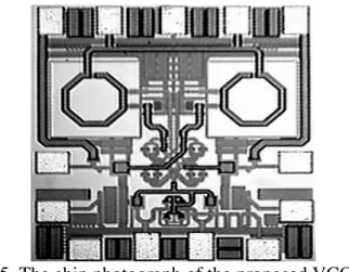
The VCO’s were fabricated by the TSMC 0.18um 1P6M CMOS technologies and the chip photo of the VCO is shown in Fig. 5. The two helical inductors are on the top side, the other circuits are on the bottom side. The circuit simulation was carried out by the simulation tool SpectreRF. The total chip area is 0.665 x 0.732 mm2 and the VCO core power consumption is approximate to 2.6 mW at 1V supply voltage. Since the helical inductor technique is also suitable for low voltage operation, different supply voltages are used to test the circuit.
Fig. 6 shows the measured output power spectrum of the 2.5-GHz oscillation signal with the output power of -14.3dBm. The phase noise at 1M offset is –116.8dBc/Hz, and the supply voltage is 1.0V. The measured tuning range is shown in Fig. 7. The tuning range is about 0.43-GHz (18%) tuning range at Vdd=1.0V. The tuning range is about 0.5-GHz (20%) tuning range at Vdd=1.5V. The varactors are accumulation mode nMOS varactors, as the gate
Fig. 5. The chip photograph of the proposed VCO.
voltage of the varactors (i.e., Vtune) increases, the varactor’s capacitance increases, therefore the oscillation frequency decreases. The inductance of the resonator is determined by the tapped inductor while the capacitance is
determined by the MOS varactors, and parasitic capacitance of the inductors, the capacitance between drain and ground of the transistors and the gate capacitance. The inductors are simulated by using the simulation tool- ADS Momentum and Spectre RF to get its related model parameters.
Fig. 8 shows the measured phase noise of the VCO.
The phase noise (A) is –116.8dBc/Hz at 1MHz offset from the oscillation frequency of 2.46GHz at Vdd=1.0V. The phase noise (B) is –116.9dBc/Hz at 1MHz offset from the oscillation frequency of 2.53GHz at Vdd=1.5V. And the measured phase noise is mainly consisted of a 1/f 3 portion. Table 1 compares these oscillators with the other oscillator published in literature. The figure of merit defined as (2)
] )
log[(
10 }
{ 2 DC
osc
f P f f
L
FOM ∆ ⋅
+
∆
= (2)
where L{∆f} is the SSB phase noise measured at ∆f offset from fosc carrier frequency and PDC is the DC power consumption in mW. As shown in Table I, the figure of merit (FOM) of the VCO is –180.25 dBc and tuning range is 18%. The data indicates that the proposed VCO circuit has a better FOM than that in [3].
Fig. 6 The output spectrum of proposed VCO.
2 2.1 2.2 2.3 2.4 2.5 2.6
0 0.2 0.4 0.6 0.8 1 1.2 1.4 1.6
Fig. 7 The tuning range of the VCO.
Fig. 8 Measured phase noise at 1MHz offset.
V. CONCLUSION
A low voltage and wide tuning range 2.4GHz VCO employing the 3D helical inductors fabricated in the 0.18-um CMOS technology has been demonstrated, the VCO circuit uses the concept of inductor tapping to shift the parasitic drain-to-bulk junction capacitances of active switching MOSFET’s away from paralleling with the varactors. The fixed capacitance that affects the tuning range is reduced, therefore the tuning range is increased. A 3D inductor reduces the chip occupied area and lowers chip cost. The implemented VCO core consumes power of 2.6mW at 1.0V supply voltage, and the measured phase noise is -116.8dBc/Hz at 1MHz offset from the oscillation frequency of 2.46GHz.
And core consumes power of 5.85mW at 1.5V supply voltage, and the measured phase noise is -116.9dBc/Hz at 1MHz offset from the oscillation frequency of 2.53GHz. The present technique applies to a corresponding p-type cross-coupled VCO to achieve a lower phase noise VCO.
Table. 1. The performance of the circuit.
This work
This work
[3]
Supply voltage
1.0 V 1.5 V 1.5 V Current 2.6mA 3.9mA 5.5mA Tuning
Range
18% 20% 16%
FOM 180.25 dBc
177.3 dBc
179.4 dBc Center
Frequency
2.4 GHz 2.53 GHz 2.4 GHz
ACKNOWLEDGMENT
The authors would like to thank CIC of National Science Council, R.O.C. for the chip implementation.
REFERENCES
[1] N. Fong, J. Kim, J.-O. Plouchart, N. Zamdmer, D. Liu, L. Wagner, C. Plett and G. Tarr, "A low-voltage 40-GHz complementary VCO with 15% frequency tuning range in SOI CMOS technology," IEEE J. Solid State Circuit, vol 39, No. 5, pp. 841-846, May 2004.
[2] J. Gil, S.-S. Song, H. Lee and H. Shin, “A -119.2 dBc/Hz at 1 MHz, 1.5 mW, fully integrated, 2.5-GHz, CMOS VCO using helical inductors,”
IEEE Microwave Wireless Compon. Lett., vol. 13, no. 11, pp. 457–459, Nov. 2003.
[3] P. W. Lai, L. Dobos, S. Long, "A 2.4GHz SiGe low phase-noise VCO using on chip tapped inductor", IEEE, ESSIRC 2003, pp. 505-508.
[4] A. Jerng, and C. G. Sodini,”The impact of device type and sizing on phase noise mechanisms”, IEEE J. Solid-State Circuits, vol. 40, pp. 360–369, 2005.
[5] M. D. Tsai, Design of 5-GHz Low-voltage and Gain-Controllable CMOS Low Noise Amplifer, M.S. Thesis, National Taiwan University, June 2003.