行政院國家科學委員會專題研究計畫 成果報告
以準分子雷射製造大晶粒低溫多晶矽膜設備研發--子計畫 二:大晶粒低溫多晶矽膜之製程設計暨膜質分析與系統評
估
研究成果報告(精簡版)
計 畫 類 別 : 整合型
計 畫 編 號 : NSC 95-2218-E-011-012-
執 行 期 間 : 95 年 08 月 01 日至 96 年 07 月 31 日 執 行 單 位 : 國立臺灣科技大學電子工程系
計 畫 主 持 人 : 葉文昌
計畫參與人員: 碩士班研究生-兼任助理:陳建州、陳秉群、金大為
報 告 附 件 : 出席國際會議研究心得報告及發表論文 出席國際會議研究心得報告及發表論文
處 理 方 式 : 本計畫可公開查詢
中 華 民 國 96 年 08 月 25 日
行政院國家科學委員會補助專題研究計畫成果報告
※※※※※※※※※※※※※※※※※※※※※※※※※※
※ 以準分子雷射製造大晶粒低溫多晶矽膜設備研發— ※
※ 子計畫二:大晶粒低溫多晶矽膜之製程設計暨膜質 ※
※ 分析與系統評估 ※
※※※※※※※※※※※※※※※※※※※※※※※※※※
計畫類別:□個別型計畫 V 整合型計畫 計畫編號:
NSC 95-2218-E-011-012執行期間: 2006 年 8 月 1 日至 2007 年 7 月 1 日
計畫主持人:葉文昌 共同主持人:
計畫參與人員:黃祥恩, 陳秉群, 戴漢昇, 金大為
執行單位:台灣科技大學
中 華 民 國 96 年 8 月 25 日
矽膜準分子雷射退火過程之橫向長晶過程量測
“Growth Rate Measurement of Lateral Grains in Silicon Film During Excimer Laser Annealing”
計畫編號:NSC 95-2218-E-011-012
執行期間:2006 年 8 月 1 日 至 2007 年 7 月 31 日 主持人:葉文昌 台灣科技大學 電子工程系教授
一、中文摘要
本研究首次即時觀測矽膜雷射退火結晶 化過程之橫向長晶, 而求出長晶速率. 本研 究使雷射退火過程中之矽膜橫向長晶週期性 發生. 當 HeNe 雷射照射到矽膜時, 此矽膜使 HeNe 雷射束產生繞射干涉現像, 而藉由以光 偵測器量測 0 次繞射強度,推算出此繞射格子 之開口率變化, 進而推算出長晶速率. 求得 之長晶速率為 5 m/s, 且得知此值不隨矽融液 過冷卻溫度而改變.
英文摘要
Direct measurement of the liquid/solid interface position history of super-lateral growth (SLG) on a silicon thin film during excimer laser crystallization was carried out for the first time.
Unidirectional lateral grains were grown periodically, and by measuring the intensity of zero-order diffraction laser light, we obtained the position history of the moving solid/melt interface. The result showed that SLG growth rate was constant at 5 m/s, regardless of the supercooling degree of the Si melt
二、計畫的緣由與目的
Excimer laser crystallization (ELC) of amorphous silicon (a-Si) thin films has been widely applied to the production of low-temperature polycrystalline silicon (poly-Si) for thin-film transistors (TFTs) on glass substrates.1,2) Scientifically, rapid melt-mediated phase transformation processes, through which ELC occurs, is of fundamental importance to the materials science community. In situ melt/solid interface probing techniques such as time-resolved electrical conductance,3) optical reflectance and transmittance, 4-9) and thermal emission10) methods have been proven to be effective for investigating the mechanisms underlying the transformation of Si films under uniform laser light distributed ELC. Recently, the study of ELC has been focused on super-lateral growth (SLG),8, 11-15)in which large grains grow laterally exhibiting a better electrical performance. There are several studies in which the mechanism underlying SLG was investigated on the bases of thermodynamic numerical simulation.16-20). However, compared with the vertical solidification in conventional ELC, there are few in situ experimental studies of SLG. This is due primarily to the insufficient spatial resolutions of the above probing techniques for studying SLG, which generally occurs within 10 μm. In this study, we propose and developed a method for direct measurement of the position history of the liquid/solid interface of SLG, and measured the growth rate of SLG.
三、研究方法及成果
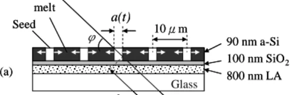
Figure 1(a) shows the schematic of the proposed method. Unidirectional lateral grains were grown periodically from preformed poly-Si seeds. Because crystalline Si is transmittable for red light and liquid Si is not transmittable, the periodical solid and liquid regions function as a multislit diffraction grating for the incident probe laser light beam. The width of the solid Si film, therefore, corresponds to the aperture a(t) of the grating. By recording the time-dependent intensity of the zero-order diffracted spectral line during excimer laser crystallization, the a(t) function can be estimated. In the experiment, the
He-Ne laser beam (LASOS,λ= 633 nm, 10 mW) with a reduced beam diameter of 0.3 mm was used as the probe laser beam. The probe laser beam was incident through the Si film at an angle φ of 40o to the film plane, and then incident into a 1-mm-diameter fast Si pin photodiode (PD) (Thorlabs, DET210, rise time = 1 ns, diameter = 1 mm), which was 280 mm away from the Si film.
The diffraction light intensity I(θ
) from a
tilted slit as a function of the diffraction angle θ can be modified from the diffraction from a perpendicular slit21), and can be calculated asfollows:
where N is the total number of slits included in the laser beam, d is the period of the slits (10 μm),and λis the wavelength (= 633 nm). For a zero-order diffraction, since θis 0, eq. (1) can be simplified to
The response of PD R(t), which can be considered to be proportional to I(t), therefore, can be shown as
where A is a constant and R0 is a bias due to noises and background. A and R0can be obtained from experiments.
, ) / 2) 2cos(
sin ( sin
) / 2) 2cos(
sin ( sin /
2)) 2cos(
sin ) ( 2 (
) / 2) 2cos(
sin ) ( 2 ( sin ) ( )
, ( ) , (
2 2
2 2 2
2 2 2
d Nd t
a t a t
a C t t
I
) 2 ( .
) ( ) (t a t 2 I
) 3 ( ,
) ( )
(t Aat 2 R0
R
XeF excimer laser Photodiode Glass 800 nm LA
100 nm SiO2
90 nm a-Si
φ 10μm
a(t)
280mm Seed
melt
a-Si film MLA
poly-Si seed Excimer laser
substrate (a)
(b)
10μm
XeF excimer laser Photodiode Glass 800 nm LA
100 nm SiO2
90 nm a-Si
φ 10μm
a(t)
280mm Seed
melt
a-Si film MLA
poly-Si seed Excimer laser
substrate (a)
(b)
10μm
Fig. 1 Schematic diagram of measurement apparatus for time-resolved optical measurement and sample structure for lateral growth (a), schematic diagram of preseeding method (b).
The sample structure is shown in Fig. 1(a).
First, an 800-nm-thick SiOxNy film with an absorption coefficient of 12000 cm-1 as the light absorptive (LA) underlayer and 100-nm-thick SiO2 film as the buffer layer were deposited successively at 250oC on a glass substrate by plasma enhanced chemical vapor deposition (PECVD) using Si(CH3)4 as the raw material22). A 90-nm-thick amorphous Si (a-Si) film was then deposited at 200oC by Ar DC sputtering.
The LA underlayer was used for increasing SLG grain size.23) SLG grains were grown periodically by the micro melt seeding method15). This method involves the preseeding process and postgrowth process. In the preseeding process [Fig. 1(b)], a 50 mJ/cm2 intense excimer laser light was irradiated onto an a-Si film through a cylindrical microlens array (MLA) with an interval between MLA and the Si film with a
focal length of 60 μm. Then a limited region of the a-Si film on which laser light was focused can be transformed into poly-Si. A scanning electron microscopy (SEM) image of the poly-Si region is shown in Fig. 2 (a). The width of the poly-Si region was 2 μm. This poly-Si region works as the seed in the successive postgrowth process. In the subsequent postgrowth process [Fig. 1(a)], a single pulse of 351nm XeF excimer laser light (pulse duration = 25 ns) was irradiated from underneath the substrate to completely melt the a-Si film, then lateral grains grew from the seed region toward the Si melt.
This SLG process was simulated numerically on the bases of a simulation model described in ref. 18. The sample structure was the same as that used in this experiments [Fig.
1(a)]. The width of the poly-Si seed was 2 μm.
Spacially uniformly distributed excimer laser light was irradiated on to the Si film from underneath the substrate. Note that Jackson’s model of grain growth was applied in this simulation, i.e., the growth rate as a function of the temperature
T, v
g(T),
was written as follows24):where NSand NLare the numbers of atoms at the interface in the solid and liquid states respectively, V0 the atomic volume in the solid,
A
M and AF the accommodation coefficient for melting and freezing, respectively, GM and GFthe geometric factor for atoms leaving the solid state and atoms leaving the liquid state, respectively, and υthe Debye frequency. Note that on vg
(T), the driving force of grain growth is
the supercooling temperatureT, and thus the
greater the supercooling temperatureT, the
larger vg(T).
Figure 3 shows simulated temperature profiles of the Si film in lateral direction for
) 4 ( ) / exp(
) / exp(
)
(T NV0A G Q kT NV0AG Q kT
vg S M F c L F F m Seed region
Seed region
Grain growth Grain growth
10 μm
Grain growth Grain growth
2 μm
30 μm
Lateral grains Seed regions
Round grains
~0.8 μm
(a)
(b)
(c)
Seed region Seed region
Grain growth Grain growth
10 μm
Grain growth Grain growth
2 μm
30 μm
Lateral grains Seed regions
Round grains
~0.8 μm
(a)
(b)
(c)
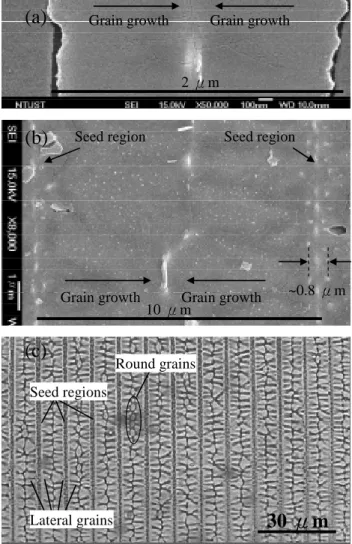
Fig. 2 (a) SEM image of seed region after preseeding process.
(b) SEM image of lateral grains after postgrowth process.
(c) Optical microphotograph of lateral grains after postgrowth process.
1500 1600 1700 1800 1900 2000 2100 2200
-5 -4 -3 -2 -1 0 1 2 3 4 5
Position (μm)
Temperature(K)
25ns
200ns 400ns 600ns 800ns 1000ns
Fig. 3 Temperature profiles of Si film in lateral
several t values. The poly-Si seed region is distributed among -1 to +1 m. The positions of the solid/melt interface are indicated by dotted arrows. After laser light irradiation, i.e., at 25 ns, the seed region (position of -1 ~ 1 m) was under a partially melting condition, whereas the rest of the region was under a completely melting condition at a temperature as high as 2200 K. This situation is due to the difference in the critical laser intensity Ic for complete melting between the a-Si film and poly-Si film. Ic of the a-Si film is about one-half that of the poly-Si film10). Because the temperature of Si melt is higher than the melting point of poly-Si, the seed region continues melting laterally from its sides even after laser irradiation. The width of the seed region decreased with increasing time and reached the minimum of 0.8 μm at 400 ns. The width of the seed region increased after t = 400 ns, owing to the formation of supercooling melts in contact with the seed. The growth rate increased with
t,
and solidification was completed at ~ 1100 ns. Note that the increasing growth rate is due to increasing supercooling temperature, because the growth rate functionv
g(T) in eq. (4) is temperature-dependent.
Figures 2(b) and 2(c) show the SEM and optical microscopy images of lateral grains after postgrowth process, respectively. Lateral grains grow from the seed regions and impinge with other lateral grains that grow from the adjoining seed regions. The position fluctuation of impingement point among all lateral grains was almost within ± 0.5 m away from the midpoint of adjoining seed regions. Because the average length of lateral grains was ~ 5 μm, the tolerance of vg
(t) is less than ± 10%. As can be noted from
Fig. 2(b) the width of a remaining seed region is about 0.8 μm (the lateral grains grew from the side of the seed), which is smaller than that shown in Fig. 2(a). This suggests the occurrence of lateral melting of the seed region during the postgrowth process. However, a few round grains [see Fig. 2(c)] exist at the midpoint of adjoining seed regions. These round grains likely originated from spontaneous nucleation.Nevertheless, we think that the effect on diffraction is limited because 1. the spontaneous nucleation take place only at the final stage of lateral growth, and the amount of lateral grains
whose lateral growth was disturbed is smaller than 12%.
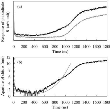
Figure 4(a) shows the response of the PD
R(t), of the Si film with (black line) and without
(gray line) preseeding. For the sample without preseeding, R(t) increased at around 1000 ns.This is because spontaneous nucleation takes place in the Si melt; therefore, grains started to grow from these spontaneously formed nuclei.
R(t) decreased its gradient at 1300 ns. This is due
to the completion of solidification. In the Si film with preseeding, R(t) increased from 440 ns onward. Because the seeds were present in the Si film, once the supercooling melt in contact with seeds was formed, the seeds started to grow.Therefore, the R(t) increase from 440 ns onward means that the supercooling condition had occurred in the Si melt. The gradient dR(t)/dt decreased after 1300 ns owing to the completion of solidification.
The aperture
a(t)
of the slit, which corresponds to the width of the solidified region, can be derived from R(t) using eq. (3). A and R0were obtained by substituting the minimum and maximum R(t) values into eq. (3). The minimum
R(t) corresponds to the minimum a(t), i.e., 0.8
μm, whereas the maximum R(t) corresponds to the maximum a(t), i.e., 10 μm. On the basis of this, the function of a(t) was obtained and is0 200 400 600 800 1000 1200 1400 1600 1800 Time (ns)
Responseofphotodiode R(arb.unit)
0 2 4 6 8 10 12
0 200 400 600 800 1000 1200 1400 1600 1800 Time (ns)
Apartureofslitsa(um)
(a)
(b)
,
0 200 400 600 800 1000 1200 1400 1600 1800 Time (ns)
Responseofphotodiode R(arb.unit)
0 2 4 6 8 10 12
0 200 400 600 800 1000 1200 1400 1600 1800 Time (ns)
Apartureofslitsa(um)
(a)
(b)
,
Fig. 4 (a) Response of PD R(t) as a function of time with ( solid line) and without (gray line) preseeding.
(b) Aperture a(t) as a function of time for experimental results (solid line) and simulation results (gray line).
plotted in Fig. 3(b) indicated by a black line. The simulation result is also shown as a gray line for comparison.
The aperture a(t) decreased gradually from 2 to 0.8 μm from 50 to 360 ns, which is consistent with the simulation results. This also suggests the lateral melting of seed regions. At t
> 440 ns, the lateral grains started growing with
da(t)/dt remaining almost constant at 10 m/s
from 440 to 1100 ns. da(t)/dt corresponds to twofold of the lateral growth rate vg(t); therefore, v
g(t) was constant at 5 m/s among this term.
da(t)/dt increased at t > 1100 ns, which is
probably due to grain growth originating from spontaneous nucleation and resulted in the formation of round grains as shown in Fig. 2(c).This result suggests that the Si melt at 1100 ns is under a strong supercooling condition for spontaneous nucleation to occur. The temperature for spontaneous nucleation to occur is estimated to be about 500 K below the melting point25). The above-mentioned results show that either the Si melt was under a mild supercooling condition at 440 ns or under a strong supercooling condition at 1100 ns; vg
(t) was
constant. This finding disagrees with simulation results, in which vg(t) increased with increasing t.
This is due to the fact that the growth rate function vg
(T) in eq. (4) is a function of
supercooling temperature. Our experimental results, however, suggest thatv
g(T)
is independent of supercooling temperature. We have not clarified this phenomenan so far and further investigations are necessary.In conclusion, direct measurement of the liquid/solid interface position history of SLG on a silicon thin film during excimer laser crystallization was carried out for the first time.
Unidirectional lateral grains were grown periodically, and by measuring the intensity of zero-order diffraction laser light, we obtained the position history of the moving solid/melt interface. The result showed that SLG growth rate was constant at 5 m/s, and the rate was independent of the supercooling degree of the Si melt. This method is effective for studying the mechanism underlying the rapid lateral grain growth of Si thin films.
五、參考文獻
1. R. Z. Bachrach, K. Winer, J. B. Boyce, S. E. Ready, R.
I. Johnson, and G. B. Anderson: J. Electron. Mater. 19 (1990) 241.
2. T. Sameshima and S. Usui: Appl. Phys. Lett. 59 (1991) 2724.
3. M. O. Thompson, G. J. Galvin, J. W. Mayer, P. S.
Peercy, and R. B. Hammond: Appl. Phys. Lett. 42 (1983) 445.
4. K. Murakami, O. Eryu, K. Takita, and K. Masuda:
Phys. Rev. Lett. 59 (1987) 2203.
5. S. R. Stiffler and M. O. Thompson: Phys. Rev. Lett.
60 (1988) 2519.
6. G. E. Jellison, D. H. Lowndes, D. N. Mashbum, and R.
F. Wood: Phys. Rev. B 34 (1986) 2407.
7. J. Boneberg, J. Nedelcu, H. Bender, and P. Leiderer:
Mater. Sci. Eng. A 173 (1993) 347.
8. J. S. Im, H. J. Kim, and M. O. Thompson: Appl. Phys.
Lett. 63 (1993) 1969.
9. F. C. Voogt, R. Ishihara, and F. D. Tichelaar: J. Appl.
Phys. 95 (2004) 2874.
10. M. Hatano, Seungjae Moon, and Minghong Lee, Kenkichi Suzuki, and Costas P. Grigoropoulos: J.
Appl. Phys. 87 (2000) 36.
11. J. S. Im and H. J. Kim: Appl. Phys. Lett. 64 (1994) 2303.
12. M. Nakata, K. Inoue and M. Matsumura: Jpn. J. Appl.
Phys. 40 (2001) 3049.
13. P. C. van der Wilt, B. D. van Dijk, G. J. Bertens, R.
Ishihara and C. I. M. Beenakker: Appl. Phys. Lett. 72 (2001) 1819.
14. H. Kumomi: Appl. Phys. Lett. 83 (2003) 434.
15. W. Yeh and D. Ke: Jpn. J. Appl. Phys. 45 (2006) L970.
16. Vikas V. Gupta, H. Jin Song, and James S. Im: Appl.
Phys. Lett. 71 (1997) 99.
17. G. Aichmayr, D. Toet, M. Mulato, P.V. Santos, A.
Spangenberg, S. Christiansen, M. Albrecht, and H. P.
Strunk: J. Appl. Phys. 85 (1999) 4010.
18. W. Yeh and M. Matsumura: Jpn. J. Appl. Phys. 40 (2001) 492.
19. Hidayat Kisdarjono, Apostolos T. Voutsas, and Raj Solanki: J. Appl. Phys. 94 (2003) 4374.
20. C. J. Shih, C. H. Fang, C. C. Lu, M. H. Wang, M. H.
Lee, and C. W. Lan: J. Appl. Phys. 100 (2006) 053504.
21. G. R. Fowles: Introduction to Modern Optics (Holt, Rinehart and Winston, Inc., New york, USA, 1975) p.116.
22. M. Ozawa, C.H. Oh and M. Matsumura: Jpn. J. Appl.
Phys. 38 (1999) 5700.
23. W. Yeh, H. Huang, I. Niu, C. Chen: Jpn. J. Appl. Phys.
46 (2007) 1466.
24. K. Jackson and B. Chalmers: Can. J. of Phys. 34 (1956) 473.
25. S. Stiffler, M. Thompson, and P. Peercy: Phys. Rev.
43 (1991) 9851.
行政院國家科學委員會補助專題研究計畫成果報告
※※※※※※※※※※※※※※※※※※※※※※※※※※
※ 以準分子雷射製造大晶粒低溫多晶矽膜設備研發— ※
※ 子計畫二:大晶粒低溫多晶矽膜之製程設計暨膜質 ※
※ 分析與系統評估 ※
※※※※※※※※※※※※※※※※※※※※※※※※※※
計畫類別:□個別型計畫 V 整合型計畫 計畫編號:
NSC 95-2218-E-011-012執行期間: 2006 年 8 月 1 日至 2007 年 7 月 1 日
計畫主持人:葉文昌 共同主持人:
計畫參與人員:黃祥恩, 陳秉群, 戴漢昇, 金大為
執行單位:台灣科技大學
中 華 民 國 96 年 8 月 25 日
矽膜準分子雷射退火過程之橫向長晶過程量測
“Growth Rate Measurement of Lateral Grains in Silicon Film During Excimer Laser Annealing”
計畫編號:NSC 95-2218-E-011-012
執行期間:2006 年 8 月 1 日 至 2007 年 7 月 31 日 主持人:葉文昌 台灣科技大學 電子工程系教授
一、中文摘要
本研究首次即時觀測矽膜雷射退火結晶 化過程之橫向長晶, 而求出長晶速率. 本研 究使雷射退火過程中之矽膜橫向長晶週期性 發生. 當 HeNe 雷射照射到矽膜時, 此矽膜使 HeNe 雷射束產生繞射干涉現像, 而藉由以光 偵測器量測 0 次繞射強度,推算出此繞射格子 之開口率變化, 進而推算出長晶速率. 求得 之長晶速率為 5 m/s, 且得知此值不隨矽融液 過冷卻溫度而改變.
英文摘要
Direct measurement of the liquid/solid interface position history of super-lateral growth (SLG) on a silicon thin film during excimer laser crystallization was carried out for the first time.
Unidirectional lateral grains were grown periodically, and by measuring the intensity of zero-order diffraction laser light, we obtained the position history of the moving solid/melt interface. The result showed that SLG growth rate was constant at 5 m/s, regardless of the supercooling degree of the Si melt
二、計畫的緣由與目的
Excimer laser crystallization (ELC) of amorphous silicon (a-Si) thin films has been widely applied to the production of low-temperature polycrystalline silicon (poly-Si) for thin-film transistors (TFTs) on glass substrates.1,2) Scientifically, rapid melt-mediated phase transformation processes, through which ELC occurs, is of fundamental importance to the materials science community. In situ melt/solid interface probing techniques such as time-resolved electrical conductance,3) optical reflectance and transmittance, 4-9) and thermal emission10) methods have been proven to be effective for investigating the mechanisms underlying the transformation of Si films under uniform laser light distributed ELC. Recently, the study of ELC has been focused on super-lateral growth (SLG),8, 11-15)in which large grains grow laterally exhibiting a better electrical performance. There are several studies in which the mechanism underlying SLG was investigated on the bases of thermodynamic numerical simulation.16-20). However, compared with the vertical solidification in conventional ELC, there are few in situ experimental studies of SLG. This is due primarily to the insufficient spatial resolutions of the above probing techniques for studying SLG, which generally occurs within 10 μm. In this study, we propose and developed a method for direct measurement of the position history of the liquid/solid interface of SLG, and measured the growth rate of SLG.
三、研究方法及成果
Figure 1(a) shows the schematic of the proposed method. Unidirectional lateral grains were grown periodically from preformed poly-Si seeds. Because crystalline Si is transmittable for red light and liquid Si is not transmittable, the periodical solid and liquid regions function as a multislit diffraction grating for the incident probe laser light beam. The width of the solid Si film, therefore, corresponds to the aperture a(t) of the grating. By recording the time-dependent intensity of the zero-order diffracted spectral line during excimer laser crystallization, the a(t) function can be estimated. In the experiment, the
He-Ne laser beam (LASOS,λ= 633 nm, 10 mW) with a reduced beam diameter of 0.3 mm was used as the probe laser beam. The probe laser beam was incident through the Si film at an angle φ of 40o to the film plane, and then incident into a 1-mm-diameter fast Si pin photodiode (PD) (Thorlabs, DET210, rise time = 1 ns, diameter = 1 mm), which was 280 mm away from the Si film.
The diffraction light intensity I(θ
) from a
tilted slit as a function of the diffraction angle θ can be modified from the diffraction from a perpendicular slit21), and can be calculated asfollows:
where N is the total number of slits included in the laser beam, d is the period of the slits (10 μm),and λis the wavelength (= 633 nm). For a zero-order diffraction, since θis 0, eq. (1) can be simplified to
The response of PD R(t), which can be considered to be proportional to I(t), therefore, can be shown as
where A is a constant and R0 is a bias due to noises and background. A and R0can be obtained from experiments.
, ) / 2) 2cos(
sin ( sin
) / 2) 2cos(
sin ( sin /
2)) 2cos(
sin ) ( 2 (
) / 2) 2cos(
sin ) ( 2 ( sin ) ( )
, ( ) , (
2 2
2 2 2
2 2 2
d Nd t
a t a t
a C t t
I
) 2 ( .
) ( ) (t a t 2 I
) 3 ( ,
) ( )
(t Aat 2 R0
R
XeF excimer laser Photodiode Glass 800 nm LA
100 nm SiO2
90 nm a-Si
φ 10μm
a(t)
280mm Seed
melt
a-Si film MLA
poly-Si seed Excimer laser
substrate (a)
(b)
10μm
XeF excimer laser Photodiode Glass 800 nm LA
100 nm SiO2
90 nm a-Si
φ 10μm
a(t)
280mm Seed
melt
a-Si film MLA
poly-Si seed Excimer laser
substrate (a)
(b)
10μm
Fig. 1 Schematic diagram of measurement apparatus for time-resolved optical measurement and sample structure for lateral growth (a), schematic diagram of preseeding method (b).
The sample structure is shown in Fig. 1(a).
First, an 800-nm-thick SiOxNy film with an absorption coefficient of 12000 cm-1 as the light absorptive (LA) underlayer and 100-nm-thick SiO2 film as the buffer layer were deposited successively at 250oC on a glass substrate by plasma enhanced chemical vapor deposition (PECVD) using Si(CH3)4 as the raw material22). A 90-nm-thick amorphous Si (a-Si) film was then deposited at 200oC by Ar DC sputtering.
The LA underlayer was used for increasing SLG grain size.23) SLG grains were grown periodically by the micro melt seeding method15). This method involves the preseeding process and postgrowth process. In the preseeding process [Fig. 1(b)], a 50 mJ/cm2 intense excimer laser light was irradiated onto an a-Si film through a cylindrical microlens array (MLA) with an interval between MLA and the Si film with a
focal length of 60 μm. Then a limited region of the a-Si film on which laser light was focused can be transformed into poly-Si. A scanning electron microscopy (SEM) image of the poly-Si region is shown in Fig. 2 (a). The width of the poly-Si region was 2 μm. This poly-Si region works as the seed in the successive postgrowth process. In the subsequent postgrowth process [Fig. 1(a)], a single pulse of 351nm XeF excimer laser light (pulse duration = 25 ns) was irradiated from underneath the substrate to completely melt the a-Si film, then lateral grains grew from the seed region toward the Si melt.
This SLG process was simulated numerically on the bases of a simulation model described in ref. 18. The sample structure was the same as that used in this experiments [Fig.
1(a)]. The width of the poly-Si seed was 2 μm.
Spacially uniformly distributed excimer laser light was irradiated on to the Si film from underneath the substrate. Note that Jackson’s model of grain growth was applied in this simulation, i.e., the growth rate as a function of the temperature
T, v
g(T),
was written as follows24):where NSand NLare the numbers of atoms at the interface in the solid and liquid states respectively, V0 the atomic volume in the solid,
A
M and AF the accommodation coefficient for melting and freezing, respectively, GM and GFthe geometric factor for atoms leaving the solid state and atoms leaving the liquid state, respectively, and υthe Debye frequency. Note that on vg
(T), the driving force of grain growth is
the supercooling temperatureT, and thus the
greater the supercooling temperatureT, the
larger vg(T).
Figure 3 shows simulated temperature profiles of the Si film in lateral direction for
) 4 ( ) / exp(
) / exp(
)
(T NV0A G Q kT NV0AG Q kT
vg S M F c L F F m Seed region
Seed region
Grain growth Grain growth
10 μm
Grain growth Grain growth
2 μm
30 μm
Lateral grains Seed regions
Round grains
~0.8 μm
(a)
(b)
(c)
Seed region Seed region
Grain growth Grain growth
10 μm
Grain growth Grain growth
2 μm
30 μm
Lateral grains Seed regions
Round grains
~0.8 μm
(a)
(b)
(c)
Fig. 2 (a) SEM image of seed region after preseeding process.
(b) SEM image of lateral grains after postgrowth process.
(c) Optical microphotograph of lateral grains after postgrowth process.
1500 1600 1700 1800 1900 2000 2100 2200
-5 -4 -3 -2 -1 0 1 2 3 4 5
Position (μm)
Temperature(K)
25ns
200ns 400ns 600ns 800ns 1000ns
Fig. 3 Temperature profiles of Si film in lateral
several t values. The poly-Si seed region is distributed among -1 to +1 m. The positions of the solid/melt interface are indicated by dotted arrows. After laser light irradiation, i.e., at 25 ns, the seed region (position of -1 ~ 1 m) was under a partially melting condition, whereas the rest of the region was under a completely melting condition at a temperature as high as 2200 K. This situation is due to the difference in the critical laser intensity Ic for complete melting between the a-Si film and poly-Si film. Ic of the a-Si film is about one-half that of the poly-Si film10). Because the temperature of Si melt is higher than the melting point of poly-Si, the seed region continues melting laterally from its sides even after laser irradiation. The width of the seed region decreased with increasing time and reached the minimum of 0.8 μm at 400 ns. The width of the seed region increased after t = 400 ns, owing to the formation of supercooling melts in contact with the seed. The growth rate increased with
t,
and solidification was completed at ~ 1100 ns. Note that the increasing growth rate is due to increasing supercooling temperature, because the growth rate functionv
g(T) in eq. (4) is temperature-dependent.
Figures 2(b) and 2(c) show the SEM and optical microscopy images of lateral grains after postgrowth process, respectively. Lateral grains grow from the seed regions and impinge with other lateral grains that grow from the adjoining seed regions. The position fluctuation of impingement point among all lateral grains was almost within ± 0.5 m away from the midpoint of adjoining seed regions. Because the average length of lateral grains was ~ 5 μm, the tolerance of vg
(t) is less than ± 10%. As can be noted from
Fig. 2(b) the width of a remaining seed region is about 0.8 μm (the lateral grains grew from the side of the seed), which is smaller than that shown in Fig. 2(a). This suggests the occurrence of lateral melting of the seed region during the postgrowth process. However, a few round grains [see Fig. 2(c)] exist at the midpoint of adjoining seed regions. These round grains likely originated from spontaneous nucleation.Nevertheless, we think that the effect on diffraction is limited because 1. the spontaneous nucleation take place only at the final stage of lateral growth, and the amount of lateral grains
whose lateral growth was disturbed is smaller than 12%.
Figure 4(a) shows the response of the PD
R(t), of the Si film with (black line) and without
(gray line) preseeding. For the sample without preseeding, R(t) increased at around 1000 ns.This is because spontaneous nucleation takes place in the Si melt; therefore, grains started to grow from these spontaneously formed nuclei.
R(t) decreased its gradient at 1300 ns. This is due
to the completion of solidification. In the Si film with preseeding, R(t) increased from 440 ns onward. Because the seeds were present in the Si film, once the supercooling melt in contact with seeds was formed, the seeds started to grow.Therefore, the R(t) increase from 440 ns onward means that the supercooling condition had occurred in the Si melt. The gradient dR(t)/dt decreased after 1300 ns owing to the completion of solidification.
The aperture
a(t)
of the slit, which corresponds to the width of the solidified region, can be derived from R(t) using eq. (3). A and R0were obtained by substituting the minimum and maximum R(t) values into eq. (3). The minimum
R(t) corresponds to the minimum a(t), i.e., 0.8
μm, whereas the maximum R(t) corresponds to the maximum a(t), i.e., 10 μm. On the basis of this, the function of a(t) was obtained and is0 200 400 600 800 1000 1200 1400 1600 1800 Time (ns)
Responseofphotodiode R(arb.unit)
0 2 4 6 8 10 12
0 200 400 600 800 1000 1200 1400 1600 1800 Time (ns)
Apartureofslitsa(um)
(a)
(b)
,
0 200 400 600 800 1000 1200 1400 1600 1800 Time (ns)
Responseofphotodiode R(arb.unit)
0 2 4 6 8 10 12
0 200 400 600 800 1000 1200 1400 1600 1800 Time (ns)
Apartureofslitsa(um)
(a)
(b)
,
Fig. 4 (a) Response of PD R(t) as a function of time with ( solid line) and without (gray line) preseeding.
(b) Aperture a(t) as a function of time for experimental results (solid line) and simulation results (gray line).
plotted in Fig. 3(b) indicated by a black line. The simulation result is also shown as a gray line for comparison.
The aperture a(t) decreased gradually from 2 to 0.8 μm from 50 to 360 ns, which is consistent with the simulation results. This also suggests the lateral melting of seed regions. At t
> 440 ns, the lateral grains started growing with
da(t)/dt remaining almost constant at 10 m/s
from 440 to 1100 ns. da(t)/dt corresponds to twofold of the lateral growth rate vg(t); therefore, v
g(t) was constant at 5 m/s among this term.
da(t)/dt increased at t > 1100 ns, which is
probably due to grain growth originating from spontaneous nucleation and resulted in the formation of round grains as shown in Fig. 2(c).This result suggests that the Si melt at 1100 ns is under a strong supercooling condition for spontaneous nucleation to occur. The temperature for spontaneous nucleation to occur is estimated to be about 500 K below the melting point25). The above-mentioned results show that either the Si melt was under a mild supercooling condition at 440 ns or under a strong supercooling condition at 1100 ns; vg
(t) was
constant. This finding disagrees with simulation results, in which vg(t) increased with increasing t.
This is due to the fact that the growth rate function vg
(T) in eq. (4) is a function of
supercooling temperature. Our experimental results, however, suggest thatv
g(T)
is independent of supercooling temperature. We have not clarified this phenomenan so far and further investigations are necessary.In conclusion, direct measurement of the liquid/solid interface position history of SLG on a silicon thin film during excimer laser crystallization was carried out for the first time.
Unidirectional lateral grains were grown periodically, and by measuring the intensity of zero-order diffraction laser light, we obtained the position history of the moving solid/melt interface. The result showed that SLG growth rate was constant at 5 m/s, and the rate was independent of the supercooling degree of the Si melt. This method is effective for studying the mechanism underlying the rapid lateral grain growth of Si thin films.
五、參考文獻
1. R. Z. Bachrach, K. Winer, J. B. Boyce, S. E. Ready, R.
I. Johnson, and G. B. Anderson: J. Electron. Mater. 19 (1990) 241.
2. T. Sameshima and S. Usui: Appl. Phys. Lett. 59 (1991) 2724.
3. M. O. Thompson, G. J. Galvin, J. W. Mayer, P. S.
Peercy, and R. B. Hammond: Appl. Phys. Lett. 42 (1983) 445.
4. K. Murakami, O. Eryu, K. Takita, and K. Masuda:
Phys. Rev. Lett. 59 (1987) 2203.
5. S. R. Stiffler and M. O. Thompson: Phys. Rev. Lett.
60 (1988) 2519.
6. G. E. Jellison, D. H. Lowndes, D. N. Mashbum, and R.
F. Wood: Phys. Rev. B 34 (1986) 2407.
7. J. Boneberg, J. Nedelcu, H. Bender, and P. Leiderer:
Mater. Sci. Eng. A 173 (1993) 347.
8. J. S. Im, H. J. Kim, and M. O. Thompson: Appl. Phys.
Lett. 63 (1993) 1969.
9. F. C. Voogt, R. Ishihara, and F. D. Tichelaar: J. Appl.
Phys. 95 (2004) 2874.
10. M. Hatano, Seungjae Moon, and Minghong Lee, Kenkichi Suzuki, and Costas P. Grigoropoulos: J.
Appl. Phys. 87 (2000) 36.
11. J. S. Im and H. J. Kim: Appl. Phys. Lett. 64 (1994) 2303.
12. M. Nakata, K. Inoue and M. Matsumura: Jpn. J. Appl.
Phys. 40 (2001) 3049.
13. P. C. van der Wilt, B. D. van Dijk, G. J. Bertens, R.
Ishihara and C. I. M. Beenakker: Appl. Phys. Lett. 72 (2001) 1819.
14. H. Kumomi: Appl. Phys. Lett. 83 (2003) 434.
15. W. Yeh and D. Ke: Jpn. J. Appl. Phys. 45 (2006) L970.
16. Vikas V. Gupta, H. Jin Song, and James S. Im: Appl.
Phys. Lett. 71 (1997) 99.
17. G. Aichmayr, D. Toet, M. Mulato, P.V. Santos, A.
Spangenberg, S. Christiansen, M. Albrecht, and H. P.
Strunk: J. Appl. Phys. 85 (1999) 4010.
18. W. Yeh and M. Matsumura: Jpn. J. Appl. Phys. 40 (2001) 492.
19. Hidayat Kisdarjono, Apostolos T. Voutsas, and Raj Solanki: J. Appl. Phys. 94 (2003) 4374.
20. C. J. Shih, C. H. Fang, C. C. Lu, M. H. Wang, M. H.
Lee, and C. W. Lan: J. Appl. Phys. 100 (2006) 053504.
21. G. R. Fowles: Introduction to Modern Optics (Holt, Rinehart and Winston, Inc., New york, USA, 1975) p.116.
22. M. Ozawa, C.H. Oh and M. Matsumura: Jpn. J. Appl.
Phys. 38 (1999) 5700.
23. W. Yeh, H. Huang, I. Niu, C. Chen: Jpn. J. Appl. Phys.
46 (2007) 1466.
24. K. Jackson and B. Chalmers: Can. J. of Phys. 34 (1956) 473.
25. S. Stiffler, M. Thompson, and P. Peercy: Phys. Rev.
43 (1991) 9851.
出席國際會議研究心得報告及發表論文
台灣科技大學 葉文昌
主持人在 95 年參加 International TFT conference(ITC, 歐洲羅馬, 1 月), 日期為 1 月 25~26 日. 此次並以 Oral presentation 發表研究成果.
ITC 為 2003 年由韓國及日本產學界共同催生之國際研討會, 主要領域為薄膜電晶體之相 關研究. 第一年 2003 年在韓國舉辦, 第二年 2004 年在日本九州, 第三年, 亦即此次在義大利羅 馬舉辦. 相較於往年主要由東北亞人士參加及發表, 今年由於在歐洲舉辦而多了許多歐洲人, 參加單位則有日韓 Canon, Hitachi, samsung 等大廠研發人員及學術界人員, 總發表篇數約七十 幾篇, 為歷年來最大規模之一次. 國內則除敝人以外, 交通大學亦有約 2 篇文章之發表.
研討會內容分為 poly-Si TFT, a-TFT, Oxide-TFT, Organic TFT, Flexible electronics 等. 其中 poly-Si TFT 相關論文雖然較多, 但近來似乎少些技術突破, 而相較於 poly-Si, ZnO 等
Oxide-TFT 似有突然增加之趨勢. Oxide-TFT 方面日本 Canon 團隊發表以 amorphous InZnGaO 所製作之 TFT, 移動率可達 10 cm2/vs 上下, 且由於材料為 amorphous, 因此特性均一. 此方式 還有其他優點為, 濺鍍製程, 因此可實現以塑膠為基板之可撓面板. 此外 Flexible electronics 方 面 poly-Si 有兩個發展方向, 一個是不鏽鋼片上之 LTPS-TFT 製作, 另一個是塑膠基板上之 LTPS-TFT 直接形成.
敝人此次發表雷射退火矽膜之橫向長晶過程即時量測. 這是首次利用繞射原理觀察橫向 長晶過程, 並求得橫向長晶速度為 5 m/s. 所得質疑有, 長晶速率之膜厚依存性為何? 何以速 度為定值? 等等. 此將做為進一步實驗之參考.
Location control of super lateral growth grains in excimer laser crystallization of silicon thin films by micro-light beam seeding
Wenchang Yeh, Dunyuan Ke, Mingci Zhou, Chun-Jun Zhuang, Department of Electronics Engineering
Nat’lTaiwan Univ. of Sci. &Tech., No.43, Sec. 4, Keelung, Rd, Taipei106, Taiwan E-mail: [email protected]
In this study, a novel method for location control of super lateral grains in polycrystalline Si thin films in excimer-laser crystallization was proposed and realized. No additional photolithography process is necessary in this method. Micro-melt of Si film was formed by micro-light beam. The micro-light beam was formed by focusing excimer laser by micro-lens array (MLA). One comparatively large grain or one protrusion can be formed by micro-beam irradiation with the source laser energy density of 21 and 24mJ/cm2respectively at the center of crystallized spot. Using this spot as a seed, the film was re-melted by uniform excimer laser light and super lateral growth (SLG) grains were originated from these seeds. As a result, two dimensional (2D) SLG grain location control was achieved by this method.
1. Introduction
Rapid melting and recrystallization by excimer laser laser annealing (ELA) of amorphous silicon (a-Si) thin films has been applied to the production of low-temperature polycrystalline silicon (poly-Si) for the thin-film transistors (TFTs) over glass substrates. These TFTs constitute not only the pixel switches, but also the peripheral driver circuits for active-matrix flat-panel displays. Their future evolution aims at enlargement of the matrix/circuit scale and further system integration into the panel, which demand both the enhancement of the TFT performance and the device-to-device uniformity.
However, since the carrier transport in the TFT channel is limited by an electrical potential barrier localized at the grain boundaries (GBs), poly-Si TFT has troubled with its mobility and uniformity due to the randomness of the GB location or the spatial fluctuation of the GB density within the channel. Such a trouble can be solved by single grain TFT where the channel of a TFT is fabricated within a single grain. In order to realize single grain TFT, 2 dimension (2D) location control of SLG grain in ELA should be realized. A few methods for 2D SLG grain control have been proposed in ELA of Si thin-films, μ-Cz1, phase modulated ELA (PMELA) 2 , 2D sequential lateral solidification (2D-SLS) 3 , artificial site induced crystallization4. However, complicated photolithographic processes is necessary in μ-Cz and artificial site induced crystallization, while precision excimer laser optical systems are necessary in PMELA , and 2D-SLS. In this study, a novel method for 2D location control of SLG grain was proposed and realized.
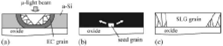
2. Experimental method
This proposed method contains pre-seeding process and post-growth process, as shown in Fig.1. In the pre seeding process(Fig1a), a μ-light beam was irradiated to the Si film to melt it in a local area. Then one grain can be formed at the center of crystallized spot. This grain work as a seed in following post-growth process. In the post-growth process, the film was molten again by uniform intensity ELA in the SLG condition. Since the larger grain is difficult to be molten compared to the small grain, part of the large grain will remain during ELA and then re-grow to become larger grain.
As for the sample preparation, 800nm-thick SiOxNyas light absorptive underlayer with the absorption coefficient of 9000cm-1 and 100nm-thick SiO2 as buffer layer were deposited successively at 250oC on glass substrate by plasma enhanced chemical vapor deposition (PECVD; hand built) using Si(CH3)4 as the raw materials. Then 90nm-thick Si was deposited at 200oC by DC Ar sputtering (hand built).
Note that the light absorptive underlayer enhanced crystallization was applied here to enlarge the grain size of SLG grain5,6,7,8.
As for the formation of μ-light beam, laser light was passed through MLA to form μ-light beam at the focal point of lens. The MLA was fabricated by reflow of photoresist (PR) and post anisotropical reactive ion etching (RIE). Hand built 3 inch RIE system was used here. Fig.2 shows the SEM image of MLA. The period of MLA was 10μm with the lens
Fig. 1 concept of proposed method
(a) Pre-seeding process. A comparatively large grain can be formed in μ-melt (b) Post-growth process. The film was re-melted by ELA except for the large grain (c) Post-growth process. SLG grain can be formed at where the μ-melt was Fig. 1 concept of proposed method
(a) Pre-seeding process. A comparatively large grain can be formed in μ-melt (b) Post-growth process. The film was re-melted by ELA except for the large grain (c) Post-growth process. SLG grain can be formed at where the μ-melt was
diameter of 8μm. The focus of this MLA was obtained experimentally and is around 50μm.
In the pre-seeding process, the MLA was put onto the surfaceofSifilm with thespaceof50μm and asingle pulse of 14~30mJ/cm2XeF excimer laser was irradiated to Si film through MLA. In the successive post-growth process, the Si film was molten by the single pulse XeF ELA in the SLG condition.
3. Experimental results
Fig.4(a) shows the SEM image of crystallized spot with laser energy density of 21mJ/cm2in pre-seeding process. We think this is in partially melting condition. This result was the same as shown grain growth mechanism in Fig. 1a.
Fig.4(b) shows the SEM image of crystallized spot with laser energy density of 24mJ/cm2in pre-seeding process. We think this is in completely melting condition, and lateral grain grow from the side of spot and impinge at the center of spot.
In the successive post-growth process, the Si film was molten by single pulse XeF excimer laser with the SLG condition. Figure 4(c) shows the SEM image of the 2D location controlled SLG after post-growth process using a seed of (a). The insert figure is a zoom of the center of grain.
There are only small defects visible and it can be concluded that the SLG grain is monocrystalline. Some protrusions can be seen at a place where the seed was, however, these protrusions seem have no influence on SLG. Figure 4(d) shows the SEM image of the 2D location controlled SLG after post-growth process using a seed under partially melting condition in pre-seeding process. The SLG grain is also monocrystalline. In this condition, the originating mechanism of SLG grain seems is different to that in using a seed under partially melting condition. The originating mechanism seems is due to the protrusion at the center of seed spot.
4. Conclusions
In conclusion, this letter presents a method of
controlling the location of crystal grains in ELA of Si thin-films. Local area of Si film was molten by micro-light beam, and one comparatively large grain was formed in the melt when the film is under the partially melt condition. In the successive process, Si was molten again, and the comparatively large grain originated the SLG grain. As a result, location controlled SLG grains with the diameter of 6μm were formed. Such a gain-location control method provides a basis for single grain TFTs, which is essential to the device–to–device uniformity of high-performance TFTs.
1 P. Ch. van der Wilt, B.D. van Dijk, G. J. Bertens, R.Ishihara and C.I.M. Beenakker: Appl. Phys. Lett. 72, 1819 (2001).
2 Mitsuru Nakata, Kouki Inoue, and Masakiyo Matsumura Jpn. J. Appl. Phys., 40, 3049 (2001).
3 James S. Im, Robert S. Sposili, and M. A. Crowder, Appl. Phys.
Lett. 70, 3434 (1997).
4. H. Kumomi, Apl. Phys. Lett. 83, 434(2003)
5 W.C. Yeh, Proceedings of the Active Matrix Liquid Crystal Display 02, 153(2002).
6. W.C. Yeh, Y. Liu, G. Chen, J. Lin, C. Chen, Y. Chen, P. Tsai, Proceedings of the Active Matrix Liquid Crystal Display 04, 247(2004).
7. W.C. Yeh, Proc. of the 1st int’l. TFT conf. 2005, 85(2005).
8. W.C. Yeh, Chun-Jun Zhuang, Guozhao Chen, Chil-Chyuan Kuo, Jeng-Ywan Jeng, Proc. of the 2nd int’l. TFT conference, (2006).
Fig.2 Fabricated micro-lens-array
10μm
Fig.2 Fabricated micro-lens-array
10μm
0.6μm6μm
50μm
Fig. 4
(a) SEM image of crystallized spot after ~21mJ/cm2μlight beam irradiation (b) SEM image of crystallized spot under ~24mJ/cm2μlight beam irradiation (c) SEM image of location controlled SLG after post -growth process of (a) seed (d) SEM image of location controlled SLG after post -growth process of (b) seed (e) OM image of location controlled SLG after post -growth process of (b) seed
0.6μm
6μm
(a) (b)
(c) (d)
(e) 0.6μm
6μm
50μm 50μm
Fig. 4
(a) SEM image of crystallized spot after ~21mJ/cm2μlight beam irradiation (b) SEM image of crystallized spot under ~24mJ/cm2μlight beam irradiation (c) SEM image of location controlled SLG after post -growth process of (a) seed (d) SEM image of location controlled SLG after post -growth process of (b) seed (e) OM image of location controlled SLG after post -growth process of (b) seed
0.6μm
6μm
(a) (b)
(c) (d)
(e)
出席國際會議研究心得報告及發表論文
台灣科技大學 葉文昌
主持人在 95 年參加 International TFT conference(ITC, 歐洲羅馬, 1 月), 日期為 1 月 25~26 日. 此次並以 Oral presentation 發表研究成果.
ITC 為 2003 年由韓國及日本產學界共同催生之國際研討會, 主要領域為薄膜電晶體之相 關研究. 第一年 2003 年在韓國舉辦, 第二年 2004 年在日本九州, 第三年, 亦即此次在義大利羅 馬舉辦. 相較於往年主要由東北亞人士參加及發表, 今年由於在歐洲舉辦而多了許多歐洲人, 參加單位則有日韓 Canon, Hitachi, samsung 等大廠研發人員及學術界人員, 總發表篇數約七十 幾篇, 為歷年來最大規模之一次. 國內則除敝人以外, 交通大學亦有約 2 篇文章之發表.
研討會內容分為 poly-Si TFT, a-TFT, Oxide-TFT, Organic TFT, Flexible electronics 等. 其中 poly-Si TFT 相關論文雖然較多, 但近來似乎少些技術突破, 而相較於 poly-Si, ZnO 等
Oxide-TFT 似有突然增加之趨勢. Oxide-TFT 方面日本 Canon 團隊發表以 amorphous InZnGaO 所製作之 TFT, 移動率可達 10 cm2/vs 上下, 且由於材料為 amorphous, 因此特性均一. 此方式 還有其他優點為, 濺鍍製程, 因此可實現以塑膠為基板之可撓面板. 此外 Flexible electronics 方 面 poly-Si 有兩個發展方向, 一個是不鏽鋼片上之 LTPS-TFT 製作, 另一個是塑膠基板上之 LTPS-TFT 直接形成.
敝人此次發表雷射退火矽膜之橫向長晶過程即時量測. 這是首次利用繞射原理觀察橫向 長晶過程, 並求得橫向長晶速度為 5 m/s. 所得質疑有, 長晶速率之膜厚依存性為何? 何以速 度為定值? 等等. 此將做為進一步實驗之參考.
Location control of super lateral growth grains in excimer laser crystallization of silicon thin films by micro-light beam seeding
Wenchang Yeh, Dunyuan Ke, Mingci Zhou, Chun-Jun Zhuang, Department of Electronics Engineering
Nat’lTaiwan Univ. of Sci. &Tech., No.43, Sec. 4, Keelung, Rd, Taipei106, Taiwan E-mail: [email protected]
In this study, a novel method for location control of super lateral grains in polycrystalline Si thin films in excimer-laser crystallization was proposed and realized. No additional photolithography process is necessary in this method. Micro-melt of Si film was formed by micro-light beam. The micro-light beam was formed by focusing excimer laser by micro-lens array (MLA). One comparatively large grain or one protrusion can be formed by micro-beam irradiation with the source laser energy density of 21 and 24mJ/cm2respectively at the center of crystallized spot. Using this spot as a seed, the film was re-melted by uniform excimer laser light and super lateral growth (SLG) grains were originated from these seeds. As a result, two dimensional (2D) SLG grain location control was achieved by this method.
1. Introduction
Rapid melting and recrystallization by excimer laser laser annealing (ELA) of amorphous silicon (a-Si) thin films has been applied to the production of low-temperature polycrystalline silicon (poly-Si) for the thin-film transistors (TFTs) over glass substrates. These TFTs constitute not only the pixel switches, but also the peripheral driver circuits for active-matrix flat-panel displays. Their future evolution aims at enlargement of the matrix/circuit scale and further system integration into the panel, which demand both the enhancement of the TFT performance and the device-to-device uniformity.
However, since the carrier transport in the TFT channel is limited by an electrical potential barrier localized at the grain boundaries (GBs), poly-Si TFT has troubled with its mobility and uniformity due to the randomness of the GB location or the spatial fluctuation of the GB density within the channel. Such a trouble can be solved by single grain TFT where the channel of a TFT is fabricated within a single grain. In order to realize single grain TFT, 2 dimension (2D) location control of SLG grain in ELA should be realized. A few methods for 2D SLG grain control have been proposed in ELA of Si thin-films, μ-Cz1, phase modulated ELA (PMELA) 2 , 2D sequential lateral solidification (2D-SLS) 3 , artificial site induced crystallization4. However, complicated photolithographic processes is necessary in μ-Cz and artificial site induced crystallization, while precision excimer laser optical systems are necessary in PMELA , and 2D-SLS. In this study, a novel method for 2D location control of SLG grain was proposed and realized.
2. Experimental method
This proposed method contains pre-seeding process and post-growth process, as shown in Fig.1. In the pre seeding process(Fig1a), a μ-light beam was irradiated to the Si film to melt it in a local area. Then one grain can be formed at the center of crystallized spot. This grain work as a seed in following post-growth process. In the post-growth process, the film was molten again by uniform intensity ELA in the SLG condition. Since the larger grain is difficult to be molten compared to the small grain, part of the large grain will remain during ELA and then re-grow to become larger grain.
As for the sample preparation, 800nm-thick SiOxNyas light absorptive underlayer with the absorption coefficient of 9000cm-1 and 100nm-thick SiO2 as buffer layer were deposited successively at 250oC on glass substrate by plasma enhanced chemical vapor deposition (PECVD; hand built) using Si(CH3)4 as the raw materials. Then 90nm-thick Si was deposited at 200oC by DC Ar sputtering (hand built).
Note that the light absorptive underlayer enhanced crystallization was applied here to enlarge the grain size of SLG grain5,6,7,8.
As for the formation of μ-light beam, laser light was passed through MLA to form μ-light beam at the focal point of lens. The MLA was fabricated by reflow of photoresist (PR) and post anisotropical reactive ion etching (RIE). Hand built 3 inch RIE system was used here. Fig.2 shows the SEM image of MLA. The period of MLA was 10μm with the lens
Fig. 1 concept of proposed method
(a) Pre-seeding process. A comparatively large grain can be formed in μ-melt (b) Post-growth process. The film was re-melted by ELA except for the large grain (c) Post-growth process. SLG grain can be formed at where the μ-melt was Fig. 1 concept of proposed method
(a) Pre-seeding process. A comparatively large grain can be formed in μ-melt (b) Post-growth process. The film was re-melted by ELA except for the large grain (c) Post-growth process. SLG grain can be formed at where the μ-melt was
diameter of 8μm. The focus of this MLA was obtained experimentally and is around 50μm.
In the pre-seeding process, the MLA was put onto the surfaceofSifilm with thespaceof50μm and asingle pulse of 14~30mJ/cm2XeF excimer laser was irradiated to Si film through MLA. In the successive post-growth process, the Si film was molten by the single pulse XeF ELA in the SLG condition.
3. Experimental results
Fig.4(a) shows the SEM image of crystallized spot with laser energy density of 21mJ/cm2in pre-seeding process. We think this is in partially melting condition. This result was the same as shown grain growth mechanism in Fig. 1a.
Fig.4(b) shows the SEM image of crystallized spot with laser energy density of 24mJ/cm2in pre-seeding process. We think this is in completely melting condition, and lateral grain grow from the side of spot and impinge at the center of spot.
In the successive post-growth process, the Si film was molten by single pulse XeF excimer laser with the SLG condition. Figure 4(c) shows the SEM image of the 2D location controlled SLG after post-growth process using a seed of (a). The insert figure is a zoom of the center of grain.
There are only small defects visible and it can be concluded that the SLG grain is monocrystalline. Some protrusions can be seen at a place where the seed was, however, these protrusions seem have no influence on SLG. Figure 4(d) shows the SEM image of the 2D location controlled SLG after post-growth process using a seed under partially melting condition in pre-seeding process. The SLG grain is also monocrystalline. In this condition, the originating mechanism of SLG grain seems is different to that in using a seed under partially melting condition. The originating mechanism seems is due to the protrusion at the center of seed spot.
4. Conclusions
In conclusion, this letter presents a method of
controlling the location of crystal grains in ELA of Si thin-films. Local area of Si film was molten by micro-light beam, and one comparatively large grain was formed in the melt when the film is under the partially melt condition. In the successive process, Si was molten again, and the comparatively large grain originated the SLG grain. As a result, location controlled SLG grains with the diameter of 6μm were formed. Such a gain-location control method provides a basis for single grain TFTs, which is essential to the device–to–device uniformity of high-performance TFTs.
1 P. Ch. van der Wilt, B.D. van Dijk, G. J. Bertens, R.Ishihara and C.I.M. Beenakker: Appl. Phys. Lett. 72, 1819 (2001).
2 Mitsuru Nakata, Kouki Inoue, and Masakiyo Matsumura Jpn. J. Appl. Phys., 40, 3049 (2001).
3 James S. Im, Robert S. Sposili, and M. A. Crowder, Appl. Phys.
Lett. 70, 3434 (1997).
4. H. Kumomi, Apl. Phys. Lett. 83, 434(2003)
5 W.C. Yeh, Proceedings of the Active Matrix Liquid Crystal Display 02, 153(2002).
6. W.C. Yeh, Y. Liu, G. Chen, J. Lin, C. Chen, Y. Chen, P. Tsai, Proceedings of the Active Matrix Liquid Crystal Display 04, 247(2004).
7. W.C. Yeh, Proc. of the 1st int’l. TFT conf. 2005, 85(2005).
8. W.C. Yeh, Chun-Jun Zhuang, Guozhao Chen, Chil-Chyuan Kuo, Jeng-Ywan Jeng, Proc. of the 2nd int’l. TFT conference, (2006).
Fig.2 Fabricated micro-lens-array
10μm
Fig.2 Fabricated micro-lens-array
10μm
0.6μm6μm
50μm
Fig. 4
(a) SEM image of crystallized spot after ~21mJ/cm2μlight beam irradiation (b) SEM image of crystallized spot under ~24mJ/cm2μlight beam irradiation (c) SEM image of location controlled SLG after post -growth process of (a) seed (d) SEM image of location controlled SLG after post -growth process of (b) seed (e) OM image of location controlled SLG after post -growth process of (b) seed
0.6μm
6μm
(a) (b)
(c) (d)
(e) 0.6μm
6μm
50μm 50μm
Fig. 4
(a) SEM image of crystallized spot after ~21mJ/cm2μlight beam irradiation (b) SEM image of crystallized spot under ~24mJ/cm2μlight beam irradiation (c) SEM image of location controlled SLG after post -growth process of (a) seed (d) SEM image of location controlled SLG after post -growth process of (b) seed (e) OM image of location controlled SLG after post -growth process of (b) seed
0.6μm
6μm
(a) (b)
(c) (d)
(e)