國立臺灣大學工學院應用力學研究所 博士論文
Institute of Applied Mechanics College of Engineering National Taiwan University
Doctoral Dissertation
研製分佈式感應子及壓電致動器應用之光壓電材料 Developing Optopiezoelectric Materials for Distributed
Sensors and Piezoelectric Actuators
張雯琪 Wen-Chi Chang
指導教授: 李世光 博士 王安邦 博士 Advisor: Chih-Kung Lee, Ph.D.
An-Bang Wang, Ph.D.
中華民國 104 年 7 月
July, 2015
i
謝誌
過去六年來,每次讀著學長姊、同學與學弟妹的畢業論文謝誌,不斷想像輪 到自己寫致謝時的心情!首先我由衷地感謝我的指導教授李世光老師與王安邦老 師。每當我面對實驗或研究生涯規畫的煩惱,不知該如何解決,李老師總會提供 許多寶貴意見使我覺得豁然開朗,讓我逐漸成為一位對光機電系統有更深體驗的 學生。另外,感謝王老師時常關心我的研究生活,而老師身體力行的學者精神,
更讓我學習做研究的態度。接著,我要感謝團隊中的林致廷老師、吳文中老師與 許聿翔老師,謝謝您們時常幫助我解決實驗問題,才使我逐步完成本篇論文。而 我也要感謝口試委員謝宗霖教授、饒達仁教授與謝志文博士,感謝您們對本篇論 文給予良好建議。
接著,我要感謝文清學長、育諺學長與順區學長,學長們總是 open-minded 告訴我如何規畫實驗與研究生活,畢業後仍時常關心我的狀況,讓我備感溫馨。
我也要謝謝實驗室一同奮鬥的 Bio 組伙伴宜靜、佩紋、柏翰、齡雅、信互、佳縉、
存勗等,大家一起為實驗努力、討論的經驗,將是我永遠美好的回憶。此外,也 感謝在 433 大家庭的好朋友仁傑、承羲、建君、富程、泓緯、則翔、冠宇、君恬、
淳惠與佩漪學姊等,以及工科 109 的立仁、欣潔、育正與俊良學長等,因為有你 們大家的陪伴,我的研究生生活也增添許多快樂的氣氛。
最後要感謝我的家人與甫諭,感謝你們一路支持,本論文也才得以完成,謹 以此文獻給每位曾經幫助我的人!
民國 104 年 7 月
ii
中文摘要
微操控技術於近年來蓬勃發展於微機電設備、生物晶片以及微流體系統。
自十九世紀末,原子力學顯微鏡、光鉗與磁鉗被實現於操控單一細胞或原子;熱 泳、介電泳與介電濕潤等非接觸式操控技術也相繼被提出,來提高控制待測物的 力量與效率,並且降低傷害樣品的風險。近年來,許多感光複合材料相繼被開發 並應用於操控技術中,使用快速變換的光照圖樣,改變晶片中局部電場或熱場,
進而達成操控微物體的效果。然而,傳統的光調變技術,僅提供或感測奈米牛頓 等級的力學場,故本論文提出光壓電複合材料,將光敏材料與壓電材料結合,藉 由照光圖樣局部調變壓電的電場與力學場,並將驅動或感測的力學場數量級提升
106數量級 。本論文於第三章,以直流偏壓 175 伏特驅動微流道系統中的壓電片,
有效侷限蠕蟲運動範圍。於第四章,使用感光染料(spiropyran)/液晶複合壓電片
(PZT),研製光壓電懸臂樑致動器,探討其位移與頻率隨紫外光(365 nm, 0.7 mW/cm2 )
照射而上升及偏移數十赫茲之機制。此外,發展光壓電感測器 P(VDF-TrFE)/
TiOPc,提出摻入 TiOPc 濃度為 10%重量百分濃度,可使材料具有最佳光調變壓電 的表現。並且於第五章,複合壓電 PZT 與 40% w.t. TiOPc/ 樹脂,研製量測誤差 小於 10%的光壓電彎曲感測器,並驗證此感測器具有快速動態調變、反應效率佳、
不影響待測物振動行為等優點,因此更能夠改善傳統力學感測器因佈點位置差異 造成的誤差。本論文透過探討壓電片於流體中的效率、研製並了解光壓電致動器 與感測器的表現,所取得的模擬、實驗及分析結果,將能作為未來創新光壓電或 光壓電流體應用之參考。
iii
關鍵字:蠕蟲侷限微流道、光壓電、光敏材料。
iv
Abstract
The micro-/ nano mechanical manipulation has been recently progressively developed for micromechanical equipment, biochips, and microfluidic devices. Since the end of the 19th century, the atomic force microscopy, optical tweezers, and magnetic tweezers have been proposed to control single cell or atom. Some indirect control methods, such as optothermal mechanism, opto-electrowetting (OEW) and optical dielectrophoresis (ODEP) techniques, provide us with larger force, better efficiency, and less damage on the objects. In these years, many optical sensitive composite materials are integrated into control systems; the electrical or thermal field can be modulated by light pattern for manipulating particles or droplets. However, these conventional optical control techniques deliver actuating or sensing force only in the nN range. In this dissertation, the optopiezoelectric actuator or sensor can modulate mN force by varying the distribution of the illuminated light pattern. In Chapter 3, a PZT actuator is triggered with 175 DC voltage in microfluidic device to efficiently trap living C.
elegans. In Chapter 4, the optopiezoelectric cantilever beam actuator of spiropyran/
liquid crystal- PZT performs UV (365 nm, 0.7 mW/cm2) modulated amplitude with few tens (Hz) frequency shift. And the P(VDF-TrFE)/ TiOPc optopiezoelectric sensors are fabricated and developed with an optimal 10 % w.t. TiOPc concentration. In traditional point bending sensor, the signal error is closely related to its position. Thus in Chapter 5, a full field optopiezoelectric bending sensor, PZT- 40% w.t. TiOPc/ resin, performs less than 10% error with numerical analysis. Without effects on the host structure, it has fast and easy modulation capability by using spatially distributed light illumination patterns. Overall, this thesis discusses the piezoelectric effect in
v
microfluidics, developing and understanding the optopiezoelectric performance. We expect the simulation, experimental and analytical results can provide some evidences and references for future innovative optopiezoelectric or optopiezoelectric fluidics application.
Keywords: Worm immobilization microfluidics, Optopiezoelectric, Photosensitive material.
Contents
口試委員會審定書 #
誌謝 i
中文摘要 ii
Abstract iv
Contents vi
List of figures ix
List of tables xvi
Chapter 1 Introduction ... 1
1.1 Micro-/ nano mechanical manipulation ………... 1
1.2 Optical manipulation for small objects ……… 3
1.3 Piezoelectric manipulation and control system ………..………. 11
1.4 Optopiezoelectric control system ………..….. 15
1.5 Motivation and purpose ………... 17
Chapter 2 Material ………... 19
2.1 Piezoelectric material ……….. 19
2.1.1 Lead Zirconium Titanate (PZT) ………. 19
2.1.2 Piezoelectric polymer ………. 20
2.2 Photoconductive material ……… 24
2.2.1 Spiropyran ……….. 24
2.2.2 Titanyl Phthalocyanine (TiOPc) ..………... 26
Chapter 3 A living worm trapper by PZT actuator ………. 28
3.1 Introduction ………. 28
3.2 Theory ……….. 31
3.2.1 A linear piezoelectric thin plate actuator ………..……….. 31
3.2.2 Laplace pressure ………. 39
3.3 Simulation ……… 40
3.4 Device fabrication ………... 50
3.5 Experimental results ……… 51
3.6 Discussion and future work ………. 54
Chapter 4 Optopiezoelectric material ……… 55
4.1 Optopiezoelectric actuator ………... 56
4.1.1 Experimental setup ………. 56
4.1.2 Results ……… 60
4.1.3 Discussion ………... 63
4.2 Optopiezoelectric sensor ………. 65
4.2.1 Material and film preparation ………. 66
4.2.2 Characterization methods ………... 67
4.2.3 Physical properties ……….. 68
4.2.4 Sensing performance ……….. 79
4.2.5 Discussion ………... 82
Chapter 5 Optopiezoelectric bending sensor ……… 83
5.1 Device fabrication and experimental setup ………. 83
5.2 Experimental results ……… 86
5.2.1 Material characteristics ………... 86
5.2.2 Bending sensor ………... 87
5.3 Numerical calculation and curve fitting ……….. 90
5.4 Discussion ……… 93
Chapter 6 Conclusion and future work ……….... 95
6.1 Conclusion ……….. 95
6.2 Future work ………. 96
Reference ………. 98
List of publications ………. 107
List of figures
Figure 1-1. Thermocapillary mechanism of to push the droplet. ………... 4 Figure 1-2. (a) The 1.53 mm radius bubble migration with temperature gradient
G=2.77 K/ mm [19]. (b) The bubbles aggregation experiment by
Hiroki Kasumi et al. [21]. ………... 4 Figure 1-3. (a) Schematic processes of laser excited bubble cavitation [22]. (b)
Schematic of the cell sorter within few microseconds response [23].
(c) The localized cell concentrator by acoustically activating the
optothermally bubbles [24]. ……… 5
Figure 1-4. The scheme of (a) a typical OEW device [29], (b) open optoelectrowetting (o-OEW) device [34], and (c) Single-sided continuous optoelectrowetting (SCOEW) working principle with its equivalent circuit model [35]. ………... 7 Figure 1-5. (a) The ODEP device for massive and parallel particles manipulation
[28]. (b) The scheme of ODEP mechanism [38]. ……… 9 Figure 1-6. The frequency response figure (not to scale) of OEW and ODEP
[41]. ………... 10
Figure 1-7. Piezoelectric effect in microfluidic device for (a) pumping [46],(b)
sorting [47], (c) mixing [49], and (d) pressure monitoring[54]. ….…. 11 Figure 1-8. Distributed piezoelectric actuators or sensors for vibration controlling
systems. ……….…….. 14
Figure 1-9. Light modulated optopiezoelectric controlling system. ………….….… 16 Figure 1-10. Overview of optical actuators and sensors for mechanical system. ….... 18
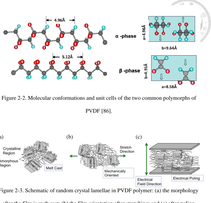
Figure 2-1. The working function of positive and converse piezoelectric effect. …. 20 Figure 2-2. Molecular conformations and unit cells of the two common
polymorphs of PVDF [86]. ………..…... 22 Figure 2-3. Schematic of random crystal lamellae in PVDF polymer. ……….. 22 Figure 2-4. Schematic structure of the molecule chain of P(VDF-TrFE) copolymer
in all-trans conformation with a ratio of VDF and TrFE of 75 : 25……. 23 Figure 2-5. The spiropyran chemical structure and some related applications. …... 24 Figure 2-6. The physical properties of titanyl phthalocyanine (TiOPc). …………... 26 Figure 2-7. Operation principle of the light-induced electric field for small
particles manipulation by Shih-Mo Yang et al. [107]. ………...…. 27 Figure 3-1. The worm image [113]. ………... 28 Figure 3-2. Methods for worm immobilization. ……… 30 Figure 3-3. The scheme of the living worm trapper with PZT actuator. …………... 31 Figure 3-4. The relationship between stress, strain, electric field, and electric
displacement. ……….. 33
Figure 3-5. (a) The deformation of a buzzer with a DC voltage, and (b) the single
layer piezoelectric actuator. ……….… 35 Figure 3-6. The unimorph piezoelectric platebefore and after deformation. ….….... 38 Figure 3-7. Interface between two immiscible fluids. ………... 39 Figure 3-8. The x- and y- directional velocities, (a) u and (b) v, when the oil bulges
expand from inlet pressure 103500 Pa at time=0.005s. ……….. 41 Figure 3-9. The volume fraction of water and oil bulges with different oil inlet
pressures (103100 Pa, 103500 Pa, 103900 Pa, 104300 Pa) at 0.005
second. ……….... 42 Figure 3-10. The volume fraction of water and FC-43 droplets with different water
inlet pressures (102700, 103500 Pa, 104300 Pa, 105100 Pa) at 0.005
second. ……….... 43
Figure 3-11. (a) The structure of the π-channel structure. (b)A real case of an extremely large bubble blocking the water channel due to Laplace
pressure. ………...………... 44
Figure 3-12. The deformation measurement from laser vibrometer (Keyence,
LK-H080). ………... 45
Figure 3-13. The x-directional velocity simulation of (a) the donut structure and (c) the fingers-donut structure with 150µm channel height. The water is static, and the oil inlet pressure is 261300 Pa. Figure (b) and (d) are the photos with water droplet at the bottom in the donut and 45°
fingers-donut structure, respectively.. ………...……….. 45 Figure 3-14. (a) The flow direction in the donat. (b)~(f) The pushing flow velocity
of the donut structure from 0.001 s to 0.005 s. ………..………... 47 Figure 3-15. The flow direction in the donut. And the pushing flow x-directional
velocity of the 30°, 45°, and 60° fingers-donut structures from 0.001 s
to 0.005 s. ……… 48
Figure 3-16. The comparison of the flow at the junctions of (a) 45° and (b) 60°
fingers-donut structure at 0.005s. .………...………… 49 Figure 3-17. (a) The fabrication process to make a microfluidic channel device with
the fingers-donut structure. (b) Photos of the front and back view of the
fingers-donut structure with 150 µm channel height. ………. 51 Figure 3-18. The steps of making oil/ water interface. (a) Let oil fill anywhere in
the channel, and then (b) pumping water into the channel. (c) The schematic of the device and the initial oil/ water interface after blocking the oil inlet. ………...……… 52 Figure 3-19. Schematic of the worm that was (a) pumped by the pipette and
swimmed into the donut structure and (b) trapped inside the water droplet. (c) The microscope image of a trapped living worm in a
water droplet. ………..………… 53
Figure 3-20. The NMR spectrum of a tube of cured PDMS. ……….. 54 Figure 4-1. The (a) double-layers and (b) single-layer photoconductive
piezoelectric composite structures. ………. 55 Figure 4-2. (a) The cell structure and (b) the SP/ LC color changes with UV
illumination. ……… 56
Figure 4-3. AVID system and its opto-mechanical setup. ………. 58 Figure 4-4. The spectra of SP/ LC with different light exposure. ……….. 60 Figure 4-5. The photo of the optopiezoelectric actuator (SP/ LC- PZT) and its
structure specification. ……… 62
Figure 4-6. The impedance of the optopiezoelectric actuator (SP/ LC- PZT) before and after UV illumination. The insert scheme is the equivalent circuit
of (SP/ LC – PZT) [71]. ……….. 62
Figure 4-7. The free-end deformation of the SP/ LC-PZT before and after UV illumination was measured by AVID. ………. 63
Figure 4-8. The scheme of the mechanism of a double-layers optopiezoelectric cantilever beam actuator. ………. 64 Figure 4-9. The deformation of a PZT buzzer with only right half electrode
triggered with 20 DC voltage. (a) COMSOL simulation; (b) Electrical speckle pattern interferometry (ESPI) measurement. ………. 65 Figure 4-10. SEM images of (a) P(VDF-TrFE) and (b)-(d) P(VDF-TrFE)/ 0.5 wt%,
2.5 wt%, 5 wt% TiOPc powder surface morphology. (e) TiPOc
powder. ………..……….. 69
Figure 4-11. FTIR transmission spectra of P(VDF-TrFE) and P(VDF-TrFE)/ TiOPc
composite film. ……… 70
Figure 4-12. XRD patterns of (a) P(VDF-TrFE) film before and after annealing.
(b) P(VDF-TrFE) and P(VDF-TrFE)/ TiOPc composite film. ………... 72 Figure 4-13. Hysteresis loops of P(VDF-TrFE) and P(VDF-TrFE)/ TiOPc
composite film. ……… 73
Figure 4-14. UV-Vis spectra of P(VDF-TrFE) and P(VDF-TrFE)/ TiOPc composite
film. ………. 75
Figure 4-15. (a) Impedance variation of P(VDF-TrFE)/ TiOPc composite film. (b) Schematic of the stimulated electrons cause the impedance variation. .. 76 Figure 4-16. The (a) resistance and (c) capacitance values of Sample 3 and Sample
6, as well as (b, d) their variation before and after illumination. ……… 76 Figure 4-17. Impedance of P(VDF-TrFE)/ 10% TiOPc at 750nm and 450nm. ……... 78 Figure 4-18. (a) The equivalent circuit of the composite. (b) Simulation and
experimental results of the impedance before and after 750nm
illumination. ……….... 78 Figure 4-19. Experimental set-up of photosensitive piezoelectric system. ... 80 Figure 4-20. Frequency spectra of the cantilever beam before and after light
illumination. ……… 80
Figure 4-21. (a) Obtained charges from the photosensitive composite piezoelectric sensor with white light illumination. (b) Scheme of charge cancellation after light illumination. ……… 81 Figure 5-1. (a) The structure and (b) mechanism of PZT-TiOPc double layers
optopiezoelectric sensor. ………. 85 Figure 5-2. The experimental setup of an optopiezoelectric sensor for measuring
bending angle. ………. 85
Figure 5-3. The calculated impedance of a 40% TiOPc film from equation 5-1 with
parameters in Table 5-1. ………. 87
Figure 5-4. The free end deflection of the one-dimensional cantilever plate under different driving forces. ……….. 88 Figure 5-5. The illuminated beam from (a) 0~14 mm, (b) 0~28 mm, and (c) 0~42
mm. (d) The excitons of the static beam with light intensity (120 klux). (e) The charges of a vibration beam at 28.6 Hz, 0.22m N with light intensity (30 klux). ………. 89 Figure 5-6. The obtained peak-to-peak charges coming from an Ag-electrode PZT
beam at different shaking forces, and also charges from a PZT-TiOPc beam with different light illumination patterns. ………. 89 Figure 5-7. The calculated charge at each section of a piezoelectric sensor
(brass-PZT-Ag). ……….. 91 Figure 5-8. The charge from measurement and expectation with α= 0.27 and β
=0.55. ……….….. 93
List of tables
Table 1-1. Comparison of force spectroscopy techniques: atomic force microscopy,
magnetic tweezers, and optical tweezers [2][3]. ……… 1
Table 2-1. The piezoelectric properties comparison of PZT and PVDF film [81]. ……… 21
Table 2-2. Comparisons of PVDF and P(VDF-TrFE) [81]. ……… 23
Table 3-1. The parameters and variables in (equation 1~ 4). ……….. 32
Table 3-2. IEEE compact matrix notation [125]. ……… 33
Table 3-3. Specifications and material properties of the π-channels structure. …... 41
Table 4-1. Infrared active modes of P(VDF-TrFE) and TiOPc. ………... 71
Table 4-2. Relationship between piezoelectric efficiency d33 values and corona charging voltage of P(VDF-TrFE) and P(VDF-TrFE)/ TiOPc composite film. ……… 74
Table 5-1. The resistor and capacitor changes of a 40% TiOPc in resin of different thicknesses [73]. ………. 86
Table 5-2. Simulation of the ratio of the slope variation, surface potential at different sections. ……….. 91
Table 5-3. The calculated charge at each section from measured Q0~42 with shaking forces 0.04 mN to 0.22 mN. ……….. 91
Table 5-4. The piezoelectric peak-to-peak charges of a general sensor and PZT-TiOPc sensor. …...………. 92
Table 5-5. The inversely calculated charges of a piezoelectric sensor from the measured charges of optopiezoelectric sensor. ……….. 94
Table 5-6. The measured surface potential of the optopiezoelectric sensor in dark. .. 94 Table 5-7. Comparison of the calculated and simulated bending slope. ………. 94
Chapter 1. Introduction
1.1 Micro-/nano mechanical manipulation
In recent years, mechanical manipulation has been widely developed in the bioengineering and microsystem fields to control small objects [1]
.
The most powerful and common techniques include atomic force microscopy (AFM), magnetic tweezers and optical tweezers (Table 1-1) [2].
Table 1-1. Comparison of force spectroscopy techniques: atomic force microscopy, magnetic tweezers, and optical tweezers [2][3].
Atomic force microscopy
Magnetic tweezers (electromagnetic tweezers)
Optical tweezers
Spatial
resolution (nm)
0.5~1 5~10 (2~10) 0.1~2
Temporal resolution (s)
10-3 10-1~10-2 (10-4) 10-4 Force range
(pN)
10~104 10-3~102 (0.01~104) 0.1~102 Displacement
range (nm)
0.5~104 5~104(5~105) 0.1~105
Probe size (µm) 100~250 0.5~5 0.25~5
Features High resolution imaging
Force clamp;
Bead rotation
Low noise; drift dumbbell geometry Limitation Large high- stiffness
probe; Large minimal force; Non specific
No manipulation (Force hysteresis)
Photo damage;
Sample heating; Non specific
Single-molecule manipulation
Atomic force microscopy (AFM), which was commercialized in 1998[4], is the most commonly used scanning probe microscope (SPM)
.
This near field technique is based on the van der Waals force between a sharp metal tip and the atoms on the sample surface. It can measure surface roughness in atomic scale resolution. In the past decades, it provides many applications in molecular metrology and biological sciences [5, 6, 7, 8]. However AFM measurements are generally at the high-force scale, its minimal force (10 pN) is too large, and it cannot provide 3D or long distance control[9].
By comparison, the magnetic tweezers, which can control the magnetic beads by permanent or electrical magnets, can measure and apply very low forces at fN. Its typical application is for cell manipulation and DNA topology [10, 11]. In addition, magnetic tweezers can also apply torques by rotating the magnetic fields [12, 13]. However, the magnetic tweezers are not as popular as AFM or optical tweezers. Because the permanent magnet configuration lacks the manipulation ability, and the electromagnet coils have significant hysteresis as a function of current [2].
Combining part of the advantages of AFM and magnetic tweezers, laser optical tweezers were proposed for particle manipulation in the 70s. Due to momentum
conservation, a highly focused laser beam provides a pico-newton attractive or repulsive force on the dielectric beads. It also gives 3D manipulation within a millisecond response for particle’s nanometer transportation, ablation, and even electron spin behavior control [14, 15, 16, 17]. But its major drawback was the high power laser spot, it might cause photo damage on the specimens. Furthermore, the direct optical force can only generate very weak force (pico Newton range). To bypass some of the limitations mentioned above, some more effective optical mechanisms and other indirect optical control techniques such as optothermal mechanism and optoelectronic tweezers are widely adopted for particle and cell manipulation.
1.2 Optical manipulation for small objects
Starting in 1980s, to overcome the force limitation of optical tweezers, an optothermal mechanism was found to provide a much larger force to allow faster droplet manipulation (cm/ s) [18]
.
One typical phenomenon is thermocapillary, which is based on the Marangoni effect (Figure 1-1). The local illuminated area has higher temperature and smaller surface stress. It means the droplet can be pumped toward the dark and cold side due to its larger surface stress. In this decade, thermocapillary can be used for fast transportation, trapping, and sorting the droplets in microfluidic studies (Figure 1-2) [19, 20, 21].
Figure 1-1. Thermocapillary mechanism of to push the droplet.
(a)
(b)
Figure 1-2. (a) The 1.53 mm radius bubble migration with temperature gradient G=2.77 K/
mm [19]. (b) The bubbles aggregation experiment by Hiroki Kasumi et al. [21].
However, the high power pulse laser still generates undesirable heat on the specimens.
Another optothermal mechanism, optothermal cavitation bubbles, was proposed around 1990s. The high power pulse laser is also used as a heating source. This focused laser produces a rapidly expanding vapor bubble in the water through nonlinear optical absorption. And then the explosive evaporation occurs when a thin layer of liquid reaches the critical temperatures in a very short period of time (Figure 1-3a) [22]. Nowadays, this pressure impulse made from the thermal-bubble is widely applied in biological chips (Figure 1-3b, 1-3c) [23, 24, 25, 26]
.
(a)
(b) (c)
Figure 1-3. (a) Schematic processes of laser excited bubble cavitation [22]. (b) Schematic of the cell sorter within few microseconds response [23]. (c) The localized
cell concentrator by acoustically activating the optothermally bubbles [24].
Although the optothermal cavitation bubbles mechanism, can indirectly generate larger force on the specimens without photo damage, the researchers continue to pursue a lower-cost and lower-power light source to access the opto-mechanical control. Since 2000s, opto-electrowetting (OEW) and optical dielectrophoresis (ODEP) techniques have been proposed to move liquid droplets and microparticleswith high performance, reliability, simplicity, and fast response. Instead of the expensive and high power (hundred milliwatts to watt) laser, the OEW and ODEP are set up with the liquid crystal displays or projectors [27].
The opto-electrowetting (OEW), which was proposed by Chiou et al. in 2003 [28], now is an effective method for manipulating micro droplets. (Figure 1-4a) depicts a typical OEW device; the droplet is sandwiched between a top hydrophobic surface and a bottom OEW surface [29, 30, 31, 32]. The bottom OEW structure is made by an
electrodes array on a photoconductive material. In the light illuminating area, the electric conductivity of the photoconductive layer increases, causing more voltage across the droplet. Base on the relationship between the contact angle θ and the applied voltage across the droplet in equation 1-1 [33], the contact angle of the droplet decrease and it moves toward the dark side.
(1-1) In equation 1-1, θ0 is the original contact angle, γ is the surface tension between the droplet and surrounding medium, ε0 is vacuum permittivity, εr is the dielectric constant, t is the thickness of the dielectric layer, and V is the voltage. Recently, many modified OEW techniques are proposed for integrating with other microfluidic components. For example, Chuang et al. presented an open optoelectrowetting (o-OEW) device with a translational speed up to 3.6 mm/ s (Figure 1-4b) [34]. Park et al. proposed the single-sided continuous optoelectrowetting (SCOEW) to overcome the droplet size limitation in the sandwich OEW device (Figure 1-4c)[35].
(a)
(b) (c)
Figure 1-4. The scheme of (a) a typical OEW device [29], (b) open optoelectrowetting (o-OEW) device [34], and (c) Single-sided continuous optoelectrowetting (SCOEW)
working principle with its equivalent circuit model [35].
Optical dielectrophoresis (ODEP) is another optoelectronic manipulation method, which was first proposed by Chiou et al. in 2005 for the parallel manipulation of single particles in (Figure 1-5a) [28]. Recently this technique is widely used in microfluidic and biological chips for cell patterning [36], sorting [37, 38], transfection [39], and separation [40]. An ODEP device consists of top and bottom transparent electrodes, and the bottom electrode is a photoconductive layer (Figure 1-5b). The photoconductive layer is used as localized virtual electrodes with incident light, making an intensive electric field in the bright area. Based on the conventional time average DEP force exerted on a sphere in a fluidic medium (equation 1-2), the particles in the aqueous can be collected in the bright areas. In this equation, R is the particle radius, εm denotes the permittivity of the liquid medium, Erms is the root-mean square magnitude of the electric field. K(ω) is the
Clausius-Mossotti (CM) factor, which is related to the particle and liquid medium’s permittivity (εp and εm), conductivity (σp and σm), and the applied frequency across the liquid medium (ω).
(1-2)
(a) (b)
Figure 1-5. (a) The ODEP device for massive and parallel particles manipulation [27]. (b) The scheme of ODEP mechanism [38].
Comparing the OEW and ODEP, due to their different working frequencies (10~20 kHz for OEW; 100~200 kHz for ODEP), the OEW is usually used for droplet manipulation,
but the ODEP can further control particles in microfluidic devices. In (Figure 1-6), below fmin, the impedance of the dielectric layer is larger than the dark impedance of the photoconductive layer (such as a-Si:H or TiOPc), so most of the voltage across the dielectric layer with or without light illumination. Between fmin and fc, under illumination, the cross voltage switch from the photoconductive layer to the dielectric layer, causing OEW to occur. Between fc and fmax, under illumination, the field now drops primarily across the liquid layer, resulting in OET. Above fmax, the impedance of the liquid becomes so low that it drops below Zl inhibiting effective voltage switching [41].
Figure 1-6. The frequency response figure (not to scale) of OEW and ODEP [41].
However, these conventional optoelectronic technologies are still only available for manipulation at nano-to sub-micro Newton scales. To obtain a better manipulation efficiency in a micro-environment, a much larger force should be discovered, developed and integrated with optical control.
1.3 Piezoelectric manipulations and control system
Over the last few decades, piezoelectric materials are widely applied in mechanical system as actuators or sensors. Piezoelectric actuators can generate small strain (usually
<0.1%) and high stress (MPa) in a fast response time, so they can provide large force but small displacement, which can do suitable pumping [42, 43, 44, 45, 46], sorting [47, 48], or mixing in microfluidic devices [49, 50]. Furthermore, based on the direct piezoelectric effect [51], some flexible and transparent piezoelectric polymers are popularly used as pressure sensors in biological researches (Figure 1-7) [52, 53, 54, 55]. These polymer films have inertness to chemical agents, high sensitivity and electrical response over a wide frequency range.
(a) (b)
(c) (d)
Figure 1-7. Piezoelectric effect in microfluidic device for (a) pumping [46],(b) sorting [47], (c) mixing [49], and (d) pressure monitoring[54].
Beside these vibration and deformation, the distributed piezoelectric elements or the so-called “smart-structures” provide the controlling ability in dynamic systems [56, 57].
Over the past 25 years, many researchers demonstrated the active control and adaptive structures with piezoelectric materials. Some early efforts focused on the integration of distributed sensors and actuators to target specific structural modes for application in sensing, actuation, or both. In 1989, Tzou et al. first derived the theories of distributed sensing and active vibration controlling for flexible shell structures [58]. In 1995, Qiu et al. controlled the bending moment of a circular cylindrical shell by the distributed inner and
outer PVDF actuators with same values but opposite phases (Figure 1-8a) [59]. Some others studies discussed the interaction between the piezoelectric material and the structure
so that they could use the piezoelectric actuators to reduce the sound pressure or vibration.
In 1991, Dimitriadis et al. demonstrated that bonding the piezoelectric elements on a plate could reduce the harmonic sound transmitted or radiated from the plate (Figure 1-8b) [60].
In 2008, Kozie’n et al. analyzed the possibility to active noise and vibration cancellation for the realistic machine structure with the distributed piezoelectric elements [61]. Recently, dell’Isola et al. proposed a damage detector which electric signals come from the state variables of the main structure and a distributed set of piezoelectric patches [62]. Wang et al. integrated piezoelectric actuating and sensing elements to be a cantilever-based
oscillating type MEMS dc current sensor [63].
Particularly in 1989, Lee and Moon introduced the patterned electrode on a continuous piezoelectric film to measure somespecific vibration modals [64, 65, 66]; these sensors with the spatialdistribution electrodes are denoted as modal sensors (Figure 1-8c) [67]. In 2001, Hsu and Lee further designed the miniature Autonomous Phase-gain ROtation/ linear Piezoelectric Optimal Sensing (APROPOS) for a fundamental a free-fall motion [68].
They also proposed a no-phase delay low-pass filter to tailor the sensor transfer function with a symmetric weighting electrode (Figure 1-8d) [69].
(a) (b)
(c)
(d)
Figure 1-8. Distributed piezoelectric actuators or sensors for vibration controlling systems.
(a) Configuration of a bending control model by Qiu et. al. [59]. (b) The sound pressure pattern of a plate vibration with and without piezoelectric actuators controlling [60]. (c) The uniform and mode 1 electrode patterns and their respective transfer functions [66]. (d) The schematic of a symmetric piezoelectric distributed sensor and its transfer function (dark
line) versus a uniform sensor (gray line) [69].
1.4 Optopiezoelectric control system
Based on the promising efficiency of piezoelectric actuators and sensors, it might be possible to develop an optical piezoelectric coupled mechanism for larger force control with novel opto-piezoelectric materials [49, 70]. Taking the convertible advantage of photoconductive materials, some photoconductive molecules are integrated with piezoelectric devices as optical virtual electrodes. In 2011, Chen et al. proposed an optically induced piezoelectric vibration control mechanism, which was achieved with a coupling of spiropyran-doped liquid crystal on PZT plates [71, 72] (Figure 1-9a). They made a mixture of liquid crystals (LC) and spiropyran (SP), then coated it onto a PZT plates as a virtual electrode. With UV light illumination, the spiropyran transfers to a polar molecule, and the impedance decreases more than one order of magnitude.
Moreover the rod-like liquid crystals can host these doped spiropyran in a good alignment.
Thus this photosensitive mixture, LC/SP, can be UV patterned for demonstrating a reversible optical controlled modal sensor.
In 2013, Huang designed a deformable mirror using a spatially modulated TiOPc/ PZT actuator [73]. A white light triggered photoconductive material, TiOPc, was coated on the
PZT buzzer as virtual electrode. By projecting different light patterns, the spatially distributed actuating forces made this TiOPc/PZT actuator deforms in respective shapes (Figure 1-9b). One year later, Chang et al. proposed an optical spatially modulated TiOPc/ piezo buzzer actuator driven by optical patterns (Figure 1-9c) [74]. By varying light illumination pattern, the spatial force enhancement was found to change the acoustic beam pattern and directivity.
(a)
(b) (c)
Figure 1-9. Light modulated optopiezoelectric controlling system. (a) Schematic of the TiOPc thin film-based optically modulated first modal sensor system [71, 72]. (b) The
spatial deformations from a spatial illuminated PZT plate by the electronic speckle pattern interferometry (ESPI) measurement [73]. (c) The acoustic beam pattern directivity of “light/ dark (LD)” and “dark/ light (DL)” of a piezoelectric speaker [74].
1.5 Motivation and purpose
These previous studies demonstrated the performance of piezoelectric sensors and actuators. They also showed the possibility of light controlled piezoelectric devices. In this study, we further discuss the capability of optical piezoelectric manipulation for distributed sensors and piezoelectric actuators. In Chapter 3, a NMR compatible C.
elegant trapper will be proposed for demonstrating the performance of PZT in microfluidic
device. In Chapter 4, a novel photoconductive piezoelectric composite (P(VDF-TrFE)/
TiOPc) will be developed and analyzed. This lead-free composite is better than PZT to be a biocompatible microfluidic chip substrate. Furthermore in Chapter 5, we will compare the mechanical sensing ability between this composite (P(VDF-TrFE)/ TiOPc) and a double layers structure (TiOPc-PZT) through a bending sensor.
Overall, we try to set out a path to achieve the optical piezoelectric manipulation and sensing (Figure 1-10). In this thesis, we demonstrate the ability of piezoelectric devices in microfluidic devices, and then developing the optopiezoelectric material for further optopiezoelectric microfluidic application.
Figure 1-10. Overview of optical actuators and sensors for mechanical system.
Chapter 2. Material
In this chapter, piezoelectric material and photoconductive material used in this study are discussed. In Chapter 3, we will integrate piezoelectric ceramic (PZT) into microfluidic device. In Chapter 4, optopiezoelectric actuator made of a spiropyran/ liquid crystal (SP/ LC) material layer on a PZT laminate will be examined. The optopiezoelectric sensor composed of piezoelectric polymer (P(VDF-TrFE) and photoconductive particles, titanyl phthalocyanine(TiOPc), are to be explored as well. In this chapter, the physical and chemical properties and applications of these materials are detailed.
2.1 Piezoelectric material
The piezoelectric effect was discovered by Pierre and Jacques Curie in 1880. But practical applications started after 1940s when sonars development started. Piezoelectric materials can be used as an actuator to transfer electrical signal into mechanical deformation (direct effect), or it can be used as a sensor to transform vibrations into electrical energy (converse effect) (Figure 2-1). The basic but detailed piezoelectric theory will be discussed in Chapter 3.
2.1.1 Lead Zirconium Titanate (PZT)
The most commercialized and widely applied piezoelectric material is lead zirconate titanate (PZT) (Pb[Zr(x)Ti(1-x)]O3). PZT has excellent piezoelectric properties, high Curies temperature (>150。C), high spontaneous polarization (remnant charge > 50 μC/cm2)
and high electromechanical coupling coefficient (d31 , d33 equal to few hundreds pC/N). It has become the basis of many important industrial products. Over the years, PZT has been applied in underwater sensors [75, 76], biosensors [77, 78], and energy harvesters [79, 80], etc.
Figure 2-1. The working function of positive and converse piezoelectric effect.
2.1.2 Piezoelectric polymer
Piezoelectric polymers have been discovered for more than 40 years, but in recent years they have progressively developed due to its flexible, lightweight and transparent advantages. The properties of polymers are very different from PZT in (Table 2-1). The piezoelectric polymers have much higher piezoelectric stress constant (g31), which indicates that they are much better sensors than ceramics [81]. Polymers also typically possess high dielectric breakdown and high operating field strength, which means they can withstand much higher driving fields than ceramics. Furthermore, with spin coating or electro spinning process, different mechanical properties and applications of the piezoelectric
polymer can be fabricated by using the sol-gel processes [82, 83]. Thus piezoelectric polymers surely establish its technical applications and useful device configurations.
Table 2-1. The piezoelectric properties comparison of PZT and PVDF film [81].
Nowadays, Poly(vinylidene fluoride) (PVDF) is one of the most applied piezoelectric polymers. It was found in 1969 to have a very large piezoelectric coefficient 6- 7 pC/N [84, 85]. Its chemical structure of (-CH2-CF2-) repeat units provides large chain flexibility. The highly repulsive forces of the fluorine atoms making the polymer polarized naturally (Figure 2-2). The most common and thermodynamically stable phase is the α-phase, which has a trans-gauche (TGTG') conformation and does not show a net lattice polarization, i.e., this phase presents no piezoelectric effect. After stretching and poling processes, the α-phase transfers to β-phase in an all-trans (TTTT) zig-zag conformation (Figure 2-3). The C-F dipoles all align in the same direction providing the β-phase PVDF a spontaneous lattice polarization, which is necessary to ferroelectric effect [86].
Property PZT PVDF
Density (103kg/m3) 7.5 1.78
Relative Permittivity ε/ ε0 1200 12
d31 (pC/N) 110 23
g31 (10-3Vm/N) 10 216
k31(%) 30 12
Acoustic Impedance
(Mkg/m2sec) 30 2.7
Features Brittle, heavy, toxic Flexible, lightweight, low mechanical impedance
Figure 2-2. Molecular conformations and unit cells of the two common polymorphs of PVDF [86].
(a) (b) (c)
Figure 2-3. Schematic of random crystal lamellae in PVDF polymer: (a) the morphology after the film is melt cast; (b) the film orientation after stretching; and (c) after poling
through the film thickness[87].
In the last decade, copolymers of PVDF with trifluoroethylene (TrFE) (-CHF-CF2-) containing different mole fractions of both components have been studied extensively. It is because they exhibit certain advantages over pure PVDF. P(VDF-TrFE) is synthesized by copolymerization VDF and TrFE monomers (Figure 2-4). Due to the higher repulsive forces of one more fluorine atoms, the ferroelectric phase is inherent in the copolymer at
room temperature. Unlike typical PVDF must be stretched, P(VDF-TrFE) can achieve β-phase conformation by only poling with a high electric field (in the order 50 MV/m) [88~
92]. More piezoelectric properties of PVDF and P(VDF-TrFE) are compared in (Table 2-2).
Figure 2-4. Schematic structure of the molecule chain of P(VDF-TrFE) copolymer in all-trans conformation with a ratio of VDF and TrFE of 75 : 25.
Table 2-2. Comparisons of PVDF and P(VDF-TrFE) [81]
Parameter Symbol and Unit PVDF P(VDF-TrFE)
Young’s modulus (109 N/m2) 2~4 3~5
Relative
Permittivity ε/ ε0 12 7
Breakdown voltage (V/µm), DC at 25。C 2000 2000 Maximum
Operating Voltage (V/µm), DC at 25。C 750 750
Operating
Temperature Range (°C) -40~60 -20~70
Electromechanical
coupling factor k31(%) 12 20
Piezoelectric Strain Constant
d31 (pC/N) 23 11
d33 (pC/N) -33 -38
Piezoelectric Stress g31 (10-3Vm/N) 216 162
2.2 Photoconductive material
For developing an optopiezoelectric material, the photoconductive material takes an important role for light-spatial modulation. These materials should be more conductive, i.e. their electrical impedance decreases after light illumination.
2.2.1 Spiropyran
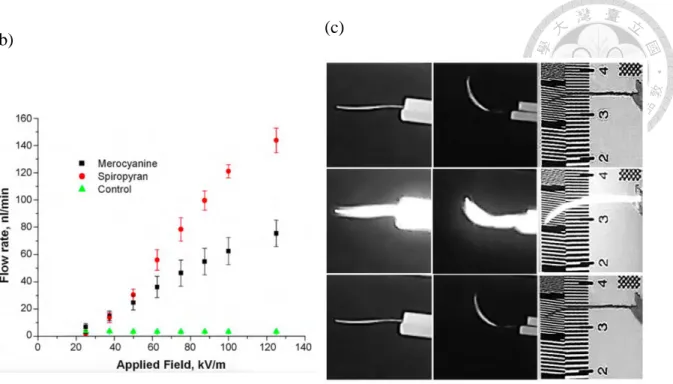
Spiropyran has been a popular photochromic material in photosensitive devices due to its advantageous physical and chemical properties [93, 94, 95]. This molecular can be transformed from a spiropyran (SP) state into a merocyanine (MC) state under UV irradiation, and it is reversible by visible light irradiation or heating (Figure 2-5a). More specifically, the carbon-oxide bond of the spiropyran is opened during transformation, which provides good ionic conductivity. Furthermore, the color also changes from light purple to a darker one under irradiation. Thus, the spiropyran molecules have widely applications include optical memories, sensors and transistors in (Figure 2-5b~ 2-5d) [96~
100].
(a)
(b) (c)
(d)
Figure 2-5. The spiropyran chemical structure and some related applications. (a) The reversible process. (b) The flow rate of photo-controllable electroosmotic in both SP and
MC form, and the poly(styrene-co-divinylbenzene) monolith using 1mM HCl as the electrolyte [98]. (c)A light activated shape memory made of spiropyran doped ethylene-vinyl acetate copolymers [99]. (d) A spiropyran modified micro-fluidic chip
channels for controlling and detecting metal ion accumulation and release [100].
2.2.2 Titanyl Phthalocyanine (TiOPc)
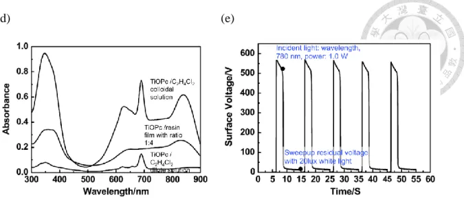
In this study, we also considered titanyl phthalocyanine (TiOPc), which is an organic photovoltaic material. TiOPc is a non-planar phthalocyanines (Pcs) with the Ti=O located slightly above (ca. 0.3Å ) the ring, orthogonal to the molecular plane (Figure 2-6a). Upon photo excitation, an electron can either move from HOMO to LUMO within a molecule (Figure 2-6b) [101]. These surprisingly close π- π molecular contacts indicate a TiOPc has a broadening of the absorbance spectrum toward the near IR region. (Figure 2-6c, 2-6d) [102]. And its high hole mobility (over 1.0 cm2 V-1 s-1) and on/off ratio make it the most efficient organic photoconductors used in more than 90% of the laser printers (Figure 2-6e)
[103]. Recently, because of its characteristics of strong illumination absorption from the visible to the IR region [104~ 106], it is also been taken in optoelectronic chip for the dynamic manipulation [107~ 109]and solar cells [110~ 112] (Figure 2-7).
(a)
Ti
C
N O
(b) (c)
(d) (e)
Figure 2-6. The physical properties of titanyl phthalocyanine (TiOPc). (a) Schematic molecular model. (b) Molecular stacking of a-TiOPc crystal showing the p-stacking structure with concave pair and convex pair with significant molecular overlaps and very short intermolecular distances [102]. (c) Schematic explaining charges excitons in TiOPc [102]. (d) UV-vis spectra of TiOPc in the colloidal solution and resin film made by Wei Chao et al. [103]. (e) The photo-induced discharging curve of a TiOPc film made by Wei
Chao et al. [103].
Figure 2-7. Operation principle of the light-induced electric field for small particles manipulation by Shih-Mo Yang et al. [107].
Chapter 3. A living worm trapper by PZT actuator
3.1 Introduction
Caenorhabditis elegans (C. elegans) (Figure 3-1) is a 1-mm long transparent
roundworm. It has a two weeks lifespan and is one of the simplest organisms for understanding cell division directly under the microscope. In the early 1960s, Sydney Brenner declared the use of C. elegans as a model to trace how genes made bodies and their behavior. In 2002, Sydney Brenner, H. Robert Horvitz and John E. Sulston received the Nobel Prize in Physiology or Medicine for their discoveries concerning "genetic regulation of organ development and programmed cell death" (an extract from The
Nobel Assembly at Karolinska Institutet, 7, October, 2002). Now the C. elegan has become a widely used model organism in biology.
Figure 3-1. The worm image [113]
Studies of C. elegans often require immobilizing the worm during monitoring or giving stimulation. Traditional techniques were based on manual manipulation on a Petri dish or a multiwall plate, and permanent immobilization for further investigations with cyanoacrylate glue or anesthetics [114, 115]. The first method consumes substantially long time, and the irreversible glues may have some toxicity. The second method gives unavoidably internal biochemical of the worm during injecting the anesthetics [116].
Currently microfluidics and micro-electromechanical system (MEMS) devices provide powerful tools and great advance for worm immobilization.
Besides using these micro chambers and pillars [117, 118], the worm immobilization can be accomplished by temperature [119] or pressure control [120], mechanical [121, 122], electrical [123], and acoustic modulation [124] (Figure 3-2a~ 3-2d).
But all these methods must maintain the pressure, temperature, or electric field continuously in order to keep the worm immobilized. They need to maintain the operation field poses a drawback for instrument such as nuclear magnetic resonance (NMR) that does not have enough spaces in the detection area for the electric wires or fluidic tubes. In this chapter, we develop an on demand piezoelectric worm trapper, which can efficiently trap the C. elegans, and keep it immobilized by hydrostatic equilibrium without using any wires, tubes, and connectors.
(a)
100µm
(b)
(c)
500 µm Before immobiliza on
During immobiliza on
(d)
Figure 3-2. Methods for worm immobilization: (a) by transiently cooling them on-chip to ~ 4 °C [119], (b) by controlling valves states sequence [120], (c) by mechanical clamping
[121], and (d) by acoustic resonance wave [122].
3.2 Theory
In this worm trapper, the worms are immobilized between oil bulges, which are pushed from the piezoelectric generated pressure (Figure 3-3). The related theories include the piezoelectric plate actuator and Laplace pressure.
Figure 3-3. The scheme of the living worm trapper with PZT actuator.
3.2.1 A linear piezoelectric thin plate actuator
The piezoelectric constitutive equations are used to calculate the transfer efficiency between electrical and mechanical signals [125]. In these equations, the piezoelectric
materials are assumed to be a linear material, which is only true when the applying electric field is small. There are four types of the equations as listed below:
Stress-Electric field type:
(3-1)
Strain-Electric field type: (3-2)
Strain-Charge type:
(3-3)
Stress-Charge type:
(3-4) The parameters and variables are detailed in (Table 3-1), and the subscripts refer to IEEE compact matrix notation in (Table 3-2) [125]. The relationships between the variables can also be represented as (Figure 3-4).
Table 3-1. The parameters and variables in (equation 1~ 4).
Symbol Name Unit Relationship
T
p Stress PaSp Strain 1
Ek Electric field V/m
Dk Electric displacement C/ m2
S
ki、kiT Dielectric or permittivity constant matrix F/m
S
ki、kiT Impermittivity constant matrix m/F
E
cpq、cDpq Elastic stiffness matrix Pa
E
spq、sDpq Elastic compliance matrix 1/Pa
dkp、
dkq Piezoelectric strain/ charge constant C/N dkp kiTgip m/V dkp e skq qpE
ekp、ekq Piezoelectric stress/ charge constant
N/Vm ekp d ckq qpE C/ m2 ekp ki ipSh
gkp、
gkq Piezoelectric strain/ voltage constant
Vm/N gkp kiTdip m2/C gkph skq qpD hkp、hkq Piezoelectric stress/ voltage constant
V/m hkp ki ipSe N/C hkp g ckq qpD
Table 3-2. IEEE compact matrix notation [125].
ij or kl p or q
11 1
22 2
33 3
23, 32 4 13, 31 5 12, 21 6
Electric field
Ek
Stress Tp
Electric displacement
Dk
Strain Sp
Figure 3-4. The relationship between stress, strain, electric field, and electric displacement.
In this study, we used a commercial buzzer (Figure 3-5a), which is composed of a PZT plate (ϕ= 17.5mm; h=200µm) glued onto a brass plate (ϕ= 12.5mm; h=100µm) as an actuator. With applied voltage, the PZT material stretches, and the stress transfers to the connected brass layer. The deformation can be clearly analyzed by a simplified modal (Figure 3-5b) [126, 127]. The displacement at the interface can be represented as (equation 3-5):
(3-5)
(0)
ui
and
(0)
u3
are the stretch and bending displacement of the interface. From (equation 3-5), the strain can be expressed in terms of (equation 3-6):
(3-6)
For an isotropic piezoelectric plate, the strain and stress are related in (equation 3-7), which Si is stress, Ti is strain, sij is elastic compliance constant, s66 2(s11s12)
, and
3 / c
E V h . If the thickness of the plate is too thin to negligible, and the stress along z-direction T3 is zero, then (equation 3-7) can also be written as (equation 3-8) with elastic stiffnessconstant (cij) and piezoelectric stress/ charge constant (eij). Thus the piezoelectric constitutive (equation 3-3, 3-4) can be written as (equation 3-9).
1= 11 1 12 2 13 3 31 3
S s T s T s T d E
(3-7)
2=12 1 11 2 13 3 31 3
S s T s T s T d E
6 66 6
S s T
(3-8)
12 66 6
T c Sp
3 31( 1 2) 33 3 31p( 1 2) 33p 3
D d T T E e S S E (3-9)
(a)
ΦCu ΦPZT
tCu
tPZT
ϕCu (mm) ϕpzt (mm) tCu(µm) tPZT(µm)
17.5 12.5 100 200
+ -
+ -
(b)
Figure 3-5. (a) The deformation of a buzzer with a DC voltage, and (b) the single layer piezoelectric actuator.
For an isotropic metal plate, its stress equation is the same as (equation 3-8). If the PZT layer is very thin, the electric field E3 is independent to the z-direction, the stretch can be written as (equation 3-10). The superscript “^” means the material parameters without applied electric field.
1,1
(0) (0) (0) (0) (0)
11 11 3 11 12 2,2 11 3,11 12 3,22 31 3
l p
l c
T T dx a u a u b u b u l e E
(3-10)1,1
(0) (0) (0) (0) (0)
22 22 3 12 11 2,2 11 3,11 12 3,22 31 3
l p
l c
T T dx a u a u b u b u l e E
(0) (0) (0) (0)
12 l 12 3 66( 1,2 2,1) 2 66 3,12
T lT dx a u u b u
where
11 11p c ˆ11p m
a c l c l , a12 c l12p cc lˆ12p m
11 12
66 66 66
( )
ˆ 2
p p
c m
a a
a c l c l
11 11 11
1( ˆ ) 2
p p
b c c l lc m
, 12 12 12
1( ˆ ) 2
p p
b c c l lc m
11 12
66 66 66
1( ˆ ) ( )
2 2
p p
c m
b b
b c c l l
The bending stress of the composite structure is shown in (equation 3-11):
1,1
(1) (0) (0) (0) (0)
11 11 3 3 11 12 2,2 11 3,11 12 3,22 31 3
l p
l c m
T T x dx b u b u u u l l e E
(3-11)
1,1
(1) (0) (0) (0) (0)
22 22 3 3 12 11 2,2 12 3,11 11 3,22 31 3
l p
l c m
T T x dx b u b u u u l l e E
(1) (0) (0) (0)
12 l 12 3 3 66( 1,2 2,1) 2 66 3,12
T lT x dx b u u u
where
![Figure 3-1. The worm image [113]](https://thumb-ap.123doks.com/thumbv2/9libinfo/9603489.629837/48.918.298.620.688.1028/figure-the-worm-image.webp)
![Table 3-2. IEEE compact matrix notation [125]. ij or kl p or q 11 1 22 2 33 3 23, 32 4 13, 31 5 12, 21 6 Electric field E k Stress Tp Electric d](https://thumb-ap.123doks.com/thumbv2/9libinfo/9603489.629837/53.918.240.709.120.984/table-ieee-compact-matrix-notation-electric-stress-electric.webp)