Electroluminescence at Si band gap energy based
on metal–oxide–silicon structures
Ching-Fuh Lin,a)C. W. Liu, Miin-Jang Chen,b)M. H. Lee, and I. C. Lin
Department of Electrical Engineering, National Taiwan University, Taipei, Taiwan, Republic of China 共Received 11 August 1999; accepted for publication 14 March 2000兲
Room-temperature electroluminescence corresponding to Si band gap energy from metal–oxide– semiconductor structures on both p-type and n-type Si is observed. With very thin oxide grown by rapid thermal oxidation, the metal–oxide–semiconductor structures behave like light emitting diodes. Luminescence is observed under forward bias even with a current density as low as 0.67 A/cm2. The physical reason for the electroluminescence is discussed and attributed to the localized wave function that leads to the spread of momentum. As a result, the spread momentum causes the electron–hole radiative recombination to occur relatively easily. © 2000 American Institute of
Physics. 关S0021-8979共00兲04612-0兴
Silicon is the most important semiconductor material for the integrated-circuit industry. However, its indirect band gap makes it hardly emit light, leading to limited applica-tions of silicon in areas of optics and optoelectronics. For decades, many efforts had been devoted to converting silicon to a light-emitting material or causing luminescence on sili-con substrates. Those efforts include porous silisili-con-based devices,1–3 nanocrystalline Si,4,5 Si⫹-implanted SiO2,6,7 Er-doped Si,8,9deposition of polymer on Si substrates,10growth of GaN on Si substrates,11,12 and so on. Recently, visible electroluminescence had also been reported from an Ag/SiO2/Si structure or similar metal–oxide–semiconductor
共MOS兲 structures with native oxide.13,14
Among them, the obstacle of the indirect-band gap nature of Si was never cir-cumvented, so no emission corresponding to band gap en-ergy occurred. In this article, we report that MOS structures on Si with the oxide grown by well-controlled rapid thermal oxidation 共RTO兲 could have the emission corresponding to band gap energy of Si. The physical reason is discussed.
MOS structures that exhibit electroluminescence have very thin oxide grown by RTO at 900 °C. The gas flows are 500 sccm nitrogen and 500 sccm oxygen at the pressure of 500 mbar. Two types of samples had been experimentally investigated. They were grown on p-type and n-type Si with the oxide of 2.3 and 3.3 nm, respectively. The thickness was measured by ellipsometry and confirmed by x-ray reflectiv-ity. The resistivity of the 100 mm p-type and n-type 共100兲 wafers used in this study is 1–5 ⍀ cm and 1–10 ⍀ cm, respectively. Aluminum metal pads were then immediately deposited by evaporation on the oxide.
A typical continuous wave共cw兲 current–voltage (I – V) curve of the MOS on p-type Si without cooling is shown in Fig. 1, showing fair rectification characteristics. The voltage was applied between metal and Si. For the MOS on p-type Si, significant current could flow through when the metal is negatively biased and vice versa for the MOS on n-type Si.
Adapting the terminology of conventional diodes, we name this condition as forward bias and the opposite bias as re-versed bias. The MOS on n-type Si has a similar I – V curve except that its turn-on voltage is smaller because the Al Fermi level (Ef m) is closer to the valence band of Si than the
conduction band.
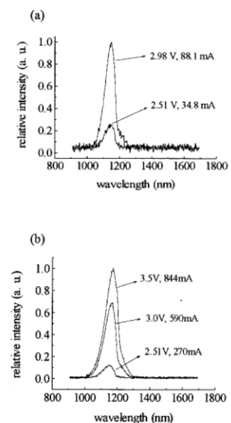
Under the forward bias, luminescence was clearly ob-served through an infrared viewer even with a current den-sity as low as 0.67 A/cm2. In the reversed bias, no lumines-cence was observed. The emission spectra were measured using a monochromator from the circular area of 2 mm di-ameter. Figures 2共a兲 and 2共b兲 show the measured spectra with the emission centered around 1150 and 1180 nm for the MOS on p-type and n-type Si, respectively, under cw opera-tion without cooling. Both correspond to the band gap en-ergy Eg of Si slightly above the room temperature. The longer wavelength for the MOS on n-type Si is probably caused by the heating effect as a result of larger injection currents.
Different from other reports,13–15 no visible lumines-cence was measured from our devices. The previously re-ported visible luminescence from the MOS with native oxide15,16is probably due to luminescent centers or oxygen deficient defects in the native oxide. In our devices, because the oxide was grown by well-controlled RTO, it should have much less defect than the native oxide. Thus, visible lumi-nescence is not observed.
Because the peak wavelength is longer than 1100 nm, the output power was measured using an InGaAs detector. Figure 3 shows the measured L – I curve for the MOS on
p-type Si under cw operation without cooling. The curve
shows a superlinear increase of the output power with the injection current. Because the Al pads are very thick, the light was observed to emit only from the periphery. If trans-parent electrodes were used, the output power should signifi-cantly increase.
The physical reason for the emission around Eg is dis-cussed as follows. The discussion is based on the MOS on
p-type Si only because the physical reason for the MOS on n-type Si is similar. For the MOS on p-type Si, Ef mincreases
a兲Also at Graduate Institute of Electro-Optical Engineering. Electronic mail:
b兲Also at Graduate Institute of Electro-Optical Engineering.
JOURNAL OF APPLIED PHYSICS VOLUME 87, NUMBER 12 15 JUNE 2000
8793
0021-8979/2000/87(12)/8793/3/$17.00 © 2000 American Institute of Physics
with the forward bias. Electrons then tunnel from metal to Si and holes tunnel from Si to metal. Theoretical analysis had shown that the major contribution of current comes from the tunneling of electrons instead of holes for the MOS on
p-type Si.17 Therefore, as Ef m moves up to the conduction
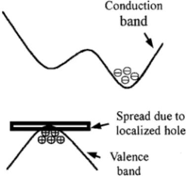
band edge (Ec), the tunneling current increases significantly because the tunneling electrons could fill in many suddenly appeared states in the conduction band. The large current causes the applied voltage indicated in Figs. 1 and 2 to drop mostly across the resistance part in the substrate, so the volt-age across the oxide is still less than the breakdown voltvolt-age of oxide. On the other hand, the negative bias of metal causes the band of the p-type silicon to bend up near the Si/SiO2 interface, as schematically shown in Fig. 4, leading
to the formation of a potential well for hole confinement. An accumulation layer of holes near the interface is then formed.
Consequently, huge population of the holes and the tunneling electrons simultaneously appear in the well region.
Although there are many electrons and holes in the same region, radiative recombination in the indirect-band gap ma-terial does not necessarily happen because the momentum still has to be conserved. However, the requirement of mo-mentum conservation could be relaxed if some mechanisms are provided in the structure. The possible reasons for pro-viding extra momentum to make radiative recombination happen are discussed in the following.
The hole in the accumulation region of the p-type semi-conductor is confined in the Si/SiO2interface, and its wave
function becomes localized. The localization of the hole cre-ates the spread of lattice momentum in the reciprocal lattice due to the uncertainty principle. The momentum separation between electrons in the⌬ valleys and the holes is then re-duced to some extent, depending on the size of the hole wave function, as shown in Fig. 5. With the band filling effect, the spread of the wave function of holes in momentum space does not have to be as large as the separation of the conduction-band minimum and the valence-band maximum in Si crystal. On the other hand, even if the spread of lattice momentum is insufficient by itself to compensate for the momentum separation, it could make other mechanisms such as interface roughness, phonon, and impurity scattering more easily provide enough momentum for the radiative recombi-nation. The hole confinement should be essential to have radiative recombination since the photoluminescence on the same sample is much weaker共not detectable in our setup兲 at
FIG. 1. The cw I – V curve of the MOS structure on p-type silicon at room temperature.
FIG. 2. The measured spectra under cw operation without cooling from the MOS on共a兲 p-type Si 共b兲 n-type Si.
FIG. 3. The L – I curve of the electroluminescence from the MOS on p-type Si.
FIG. 4. A schematic of the band diagram with the metal of the MOS on p-type Si negatively biased.
8794 J. Appl. Phys., Vol. 87, No. 12, 15 June 2000 Linet al.
room temperature. The complete picture of the radiation pro-cess is not well known and is still under investigation.
The emission energy corresponding to 1150 and 1180 nm is slightly less than the Si band gap energy at the room temperature. The reasons could be threefold. First, the band gap shrinkage with the increasing carrier density18due to the band gap renormalization effect might result in the redshift. Second, the interruption of Si periodical structure at the in-terface causes band bending and the band gap shrinkage.19 Third, the sample should be heated up under the large injec-tion current, leading to the reduced band gap energy. The ohmic heat could also explain the MOS on n-type Si emitting light at a longer wavelength because a larger current is in-jected to it. On the other hand, the band-filling effect at a large injection current could cause the blueshift of the emis-sion peak,18but this effect is not sufficient to counter balance the above three factors.
In conclusion, electroluminescence corresponding to Si band gap energy from MOS structures on both p-type and
n-type Si is observed. With very thin oxide grown by RTO,
the MOS structures behave like light emitting diodes. Under
forward bias, luminescence is observed even with a current density as low as 0.67 A/cm2. The physical reason for the electroluminescence is attributed to the localized wave func-tions of holes, leading to the spread of momentum. The extra momentum required for the electron–hole radiative recombi-nation is thus provided.
This work is supported in part by the National Science Council, Taipei, Taiwan, R.O.C. under Contract Nos. 88-2218-E-002-004, NSC88-2215-E-002-021, and NSC2112-M-002-038.
1
L. T. Canham, Appl. Phys. Lett. 57, 1046共1990兲.
2N. Koshida and H. Koyama, Appl. Phys. Lett. 60, 347共1992兲.
3S. Lazarouk, P. Jaguiro, S. Katsouba, G. Masini, S. La Monica, G. Maiello, and F. Ferrari, Appl. Phys. Lett. 68, 2108共1996兲.
4
S. Schuppler et al., Phys. Rev. B 52, 4910共1995兲.
5D. B. Geohegan, A. A. Puretzky, G. Duscher, and S. J. Pennycook, Appl. Phys. Lett. 73, 438共1998兲.
6L. S. Liao, X.-M. Bao, X.-Q. Zheng, N.-S. Li, and N.-B. Min, Appl. Phys. Lett. 68, 850共1996兲.
7
W. Skorupa, R. A. Yankov, I. E. Tyschenko, H. Frob, T. Bohme, and K. Leo, Appl. Phys. Lett. 68, 2410共1996兲.
8G. Franzo, F. Priolo, S. Coffa, A. Polman, and A. Carnera, Appl. Phys. Lett. 64, 2235共1994兲.
9
M. Matsuoka and S. Tohno, Appl. Phys. Lett. 71, 96共1997兲. 10
D. R. Baigent, R. N. Marks, N. C. Greenham, R. H. Friend, S. C. Moratti, and A. B. Holmes, Appl. Phys. Lett. 65, 2636共1994兲.
11R. Birkhahn and A. J. Steckl, Appl. Phys. Lett. 73, 1700共1998兲. 12M. Garter, J. Scofield, R. Birkhahn, and A. J. Steckl, Appl. Phys. Lett. 74,
182共1999兲.
13Y. Q. Wang, T. P. Zhao, J. Liu, and G. G. Qin, Appl. Phys. Lett. 74, 3815 共1999兲.
14J. Yuan and D. Haneman, J. Appl. Phys. 86, 2358共1999兲. 15
G. F. Bai, Y. Q. Wang, Z. C. Ma, W. H. Zong, and G. G. Qin, J. Phys.: Condens. Matter 10, L717共1998兲.
16D. L. Griscom, J. Ceram. Soc. Jpn. 99, 899共1991兲.
17C. W. Liu, M. H. Lee, C. F. Lin, I. C. Lin, W. T. Liu, and H. H. Lin, 1999 IEEE International Electron Devices Meeting, Washington, DC, Decem-ber 1999.
18H. C. Casey, Jr. and M. B. Panish, Heterostructure Lasers, Part A 共Aca-demic, Orlando, FL, 1978兲.
19S. M. Sze, Physics of Semiconductor Devices共Wiley, New York, 1981兲. FIG. 5. A schematic of the spread of hole wave function in momentum
space with respect to the momentum separation between electrons in the⌬ valleys and the holes.
8795
J. Appl. Phys., Vol. 87, No. 12, 15 June 2000 Linet al.