國
立
交
通
大
學
電子工程學系 電子研究所
博 士 論 文
深次微米互補式金氧半製程之寬頻射頻接收發射器設計
Design of a Wideband RF Transceiver in a Deep Sub-micro CMOS
Process
研 究 生:施鴻源
指導教授:郭建男 教授
深次微米互補式金氧半之製程寬頻射頻接收發射器設計
Design of a Wideband RF Transceiver in a Deep Sub-micro CMOS
Process
研 究 生:施鴻源 Student:Horng-Yuan Shih
指導教授:郭建男 Advisor:Chien-Nan Kuo
國 立 交 通 大 學
電子工程學系 電子研究所
博 士 論 文
A DissertationSubmitted to Department of Electronics Engineering and Institute of Electronics
College of Electrical and Computer Engineering National Chiao Tung University
in partial Fulfillment of the Requirements for the Degree of
Doctor of Philosophy in
Electronics Engineering
March 2010
Hsinchu, Taiwan, Republic of China
深 次 微 米 互 補 式 金 氧 半 製 程 之 寬 頻 射 頻 接 收 發 射 器 設 計
研究生:施鴻源
指導教授
:郭建男
國立交通大學電子工程學系電子研究所博士班
摘
要
本論文描述一以 1.2 V 0.13 µm CMOS 製程實現,應用於超寬頻系統之寬頻射
頻接收發射器設計。接收機設計在 3~5 GHz 的頻段。整個接收機是由一 3~5 GHz
的寬頻低雜訊放大器、三階槽口濾波器、電流式的降頻混頻器與一頻寬為 250 MHz
之類比基頻電路所組成。在類比基頻的電路中,可變增益放大器與濾波器利用電
流式放大器的形式設計達到寬頻、高增益動態範圍、低雜訊與高線性度之特點。
此外一電流式 Sallen-Key 低通濾波器被設計用來有效地濾除通道外的干擾訊
號。一個六階的 Chebyshev 低通濾波器被設計用來提供通道選擇。一數位輔助的
直流偏移校正電路用來降低整個類比基頻電路的二階諧波失真。整個接收器電路
在 1.2 V 的操作電壓下消耗 100 mW。
在發射器的設計上,我們涵蓋 3~8 GHz 的頻率範圍。整個發射器電路整合了
一類比基頻電路、調變器電路、可變增益放大器、差動轉單端放大器與功率放大
器,並整合了發射訊號強度指標電路。調變器電路並包括一直流偏移消除電路來
增進其載波洩漏的抑制能力。整個發射器提供 14 dB 的發射功率可調範圍,並具
有-5 dBm 的最大發射功率與+1.5 dBm 的輸出 P1dB。藉由直流偏移消除電路可使
得載波洩漏抑制達到 40 dB。其高線性度與調變精準度使得在 480 Mb/s 下 EVM
可達-28 dB,可滿足 WiMedia Mode 1 的規格要求。整個發射器電路在 1.2 V 的
操作電壓下消耗 66 mW。
Design of a Wideband RF Transceiver in a Deep Sub-micro CMOS Process
student:
:
:
:
Horng-Yuan ShihAdvisors:
:
:
:Dr.
Chien-Nan Kuo
Department of Electronics Engineering
Institute of Electronics
National Chiao Tung University
ABSTRACT
This dissertation presents a wideband RF transceiver for
ultra-wideband (UWB) applications implemented in a 1.2 V 0.13 µm CMOS
process. The receiver design focuses on mode 1 of multi-band (MB)
orthogonal frequency division multiplexing (OFDM) UWB (3~5 GHz)
which is defined as essential band by WiMedia Alliance. The receiver
chain is composed by a broadband 3~5GHz ESD-protected low-noise
amplifier, a 3
th-order notch filter, a current-mode down conversion mixer
and a 250MHz wideband analog baseband. In the analog baseband, PGAs
and filters are carried out by current-mode amplifiers to achieve wide
bandwidth and wide dynamic range of gain, as well as low noise and high
linearity. Besides, a current-mode Sallen-Key low-pass filter is adopted
for effective rejection of out-of-band interferers. A 6
th-order Chebyshev
low-pass filter realized in G
m-C topology is designed in the baseband
chain for channel selection. Digitally-assisted DC-offset calibration
improves second-order distortion of the entire chain. The entire receiver
consumes 100 mW under a supply voltage of 1.2 V.
In the design of transmitter, we attempt to cover both mode 1 and
Band Group 3 of MB-OFDM UWB (3~8 GHz). The 3~8 GHz transmitter
chain integrates an analog baseband, an in/quadrature-phase (IQ)
modulator, a variable gain amplifier (VGA), a differential-to-single
amplifier, a power amplifier, as well as a transmitted signal strength
indicator (TSSI). The IQ modulator incorporates DC-offset cancellation
circuits to improve carrier leakage suppression. This transmitter provides
linear-in-dB output power tuning of 14 dB to fulfill the requirement of
WiMedia UWB. Measured maximum output power and OP1dB are -5
dBm and +1.5 dBm, respectively. Measured carrier leakage suppression
is over 40 dB after calibration. The high linearity and accurate IQ
modulation lead to an error vector magnitude (EVM) of -28 dB under the
data rate of 480 Mb/s in WiMedia Mode 1. The entire transmitter
consumes 66 mW under a supply voltage of 1.2 V.
誌
謝
感謝我的父母親,施國樑先生與吳梅蘭女士對我從小的付出與教導。
父親常教導我做人處世應有的態度與方法,在我工作與學業遇到瓶頸
與挫折時總是給我許多鼓勵讓我重新站起來面對挑戰。母親對於我生
活上事物總是細心關懷,並無條件地付出與支持我。另外,我要感謝
我的妻子陳雅慧,有她在背後的支持我才能順利完成學業。我的女兒
幸昀與幸玫,妳們是我的最愛。最後,感謝我的博士班與碩士班指導
老師郭建男教授與彭松村教授在研究上給我的指導與幫助。
目
目
目
目
錄
錄
錄
錄
中文 中文 中文 中文摘摘摘摘要要要要……….i 英文摘 英文摘 英文摘 英文摘要要要要………ii 誌謝 誌謝 誌謝 誌謝………...iv Contents……….v
Figures and Tables……….vii
1 Introduction……….1
1.1 Area of focus………..1
1.2 Proposed wideband RF receiver………….………..2
1.3 Proposed wideband RF transmitter………...………5
1.4 Contributions………...………...6
1.5 Overview of Dissertation……….………..7
2 Architecture and Specifications of Receiver………...9
3 Architecture and Specifications of Transmitter………..14
4 Circuit Design of Receiver……….18
4.1 RF Front-End………..18
4.1.1 Low-Noise Amplifier (LNA)…..………....18
4.1.2 Input Matching Analysis………....20
4.1.3 Gain analysis………..21
4.1.4 Third-Order Notch Filter Design……….………....22
4.2 Analog Baseband………25
4.2.1 Programmable gain Amplifiers (PGA)………..27
4.2.2 Gm-C filter………..35
4.2.3 DC-Offset Calibration……….38
5 Circuit Design of Transmitter………44
5.1 IQ Modulator….……….44
5.2 Variable gain amplifier (VGA)………46
5.3 Differential to single-ended (D-to-S) amplifier………….………...47
5.4 Power amplifiers……….………..49
5.5 Transmitted signal strength indicator (TSSI)………...………...54
6 Receiver Measurement………..56
7 Transmitter Measurement………69 8 Conclusion and Further Work………..81
Figures and Tables
Figure 1-1: Architecture of the direct-conversion RF receiver for UWB……….……..4
Figure 1-2: Architecture of the wideband RF transmitter……….…………..6
Figure 2-1: Architecture of a direct-conversion RF receiver for UWB………..……...9
Figure 2-2: Strong nearby interferers at 5GHz (WLAN 802.11a) cause serious SNR degradation at 4.5GHz channel………..12
TABLE I. Specifications of receiver……….………13
Figure 3-1: Block diagram of the wideband RF transmitter……….…………15
TABLEII. LINK BUDGET OF TRANSMITTER……….………...17
TABLE III. specifications...17
Figure 4-1: Schematic of LC ladder LNA core……….………19
Figure 4-2(a): Transformation from LPF to BPF……….………...20
Figure 4-2(b): Design method analysis for input matching of the LNA core……..…...21
Figure 4-3: Small signal model analysis for LC ladder LNA………..………...22
Figure 4-4: Proposed 3-order active notch filter (half-circuit)……….……...24
Figure 4-5: The equivalent circuit of proposed 3-order active notch filter………....…...24
Figure 4-6: Schematic of third-order active notch filter………..…...25
Figure 4-7: Block diagram of the wideband, wide dynamic range baseband chain….26 Figure 4-8: (a) Conventional CG current amplifier, (b) Proposed current amplifier with series-series feedback……….…………..28
Figure 4-9: The schematic of PGA based on current amplifier………..………...29
Figure 4-10: Simulated input impedance of PGA……….………29
Figure 4-11: Frequency response of the PGA over different gain settings…….……..30
Figure 4-12: The schematic of current-mode SK LPF……….………..33
Figure 4-13: Equivalent circuit model of the current-mode SK LPF………...34
Figure 4-14: Frequency response of the current-mode SK LPF………..………..34
Figure 4-15: The 6th–order Gm-C filter………..………35
Figure 4-16: The schematic of Gm cell in Gm-C filter……….36
Figure 4-17: The architecture of Gm–C calibration loop………...……….37
Figure 4-18: Timing diagram of Gm–C calibration………..………..38
Figure 4-19: A typical balanced current amplifier with an input referred DC-offset current……….……….39
Figure 4-20: The schematic of 1-bit quantizer (a) Auto-zeroing amplifier (b) Latch...41
Figure 4-21: The schematic of 8-bits differential DAC………..………...41
calibration……….43
Figure 5-1: Schematic of the IQ modulator………..45
Figure 5-2: Schematic of DAC……….46
Figure 5-3: Schematic of variable gain amplifier……….47
Figure 5-4: Schematic of the D-to-S voltage amplifier………48
Figure 5-5: Equivalent circuit model of the D-to-S amplifier………..49
Figure 5-6: Schematic the wideband power amplifier………..……….51
Figure 5-7: Power amplifier operates in (a) negative cycles of output waveform (b) positve cycles of output waveform………...52
Figure 5-8: Effective model of the power amplifier……….53
Figure 5-9: Simulated frequency transfer function of the power amplifier……...…….53
Figure 5-10: Distribution of power consumption in the RF transmitter………..……..54
Figure 5-11: Schematic of the TSSI………..……….55
Figure 6-1: Chip photo of the LNA with notch filter………..………57
Figure 6-2: Measurement results for input return loss and high/low gain switch……57
Figure 6-3: Measurement results for band group1 switching………...58
Figure 6-4: Measurement results of NF under different notch frequency………58
Figure 6-5: Measurement result of highest notch frequency setting………59
Figure 6-6: P1dB measurement of high gain mode and low gain mode………..60
Figure 6-7: Nonlinearity measurement results of IIP3 under out-band interferences test………61
TABLEIV. BENCHMARK OF ULTRA-WIDE-BAND LNA DESIGNS…………..………61
Figure 6-8: Die photo of the baseband chain in 0.13µm CMOS technology. The baseband chain comprises SK LPF, current-mode PGAs, 6th–order Chebyshev Gm-C filter and circuitry for Gm-C and DC-offset calibration………...63
Figure 6-9: Measured frequency response of the baseband chain. The measured pass-band edge frequency can be varying from 250MHz to 300MHz with 1pF of probe capacitance……….64
Figure 6-10: Measured out-band IIP3 (f1=400MHz, f2=790MHz) of the baseband chain under voltage gain of 73dB and pass-band edge frequency of 250MHz………65
Figure 6-11: Measured out-band IIP2 (f1=400MHz, f2=410MHz) of the baseband chain under voltage gain of 68dB and pass-band edge frequency of 250MHz………66
Figure 6-12: Measurement noise figure of the baseband chain under voltage gain of 73dB and pass-band edge frequency of 300MHz………..………67
TABLE V: Performance summary of the baseband chain and compare to [24]……..68
Figure 7-1: Photograph of the chip………..………..72
Figure 7-3 Measured output return loss of the transmitter front-end……….………...73
Figure 7-4: Measured output power, carrier suppression and sideband suppression performance at 3432MHz……….74
Figure 7-5: Measured output power, carrier suppression and sideband suppression performance at 7656MHz……….75
Figure 7-6: Measured error vector magnitude (EVM)……….……….76
TABLEVI PERFORMANCE SUMMARY………...77
TABLEVIIPERFORMANCE COMPARISON………..………78
Figure 7-7: Measured voltage gain versus gain control voltage………..………..79
Chapter 1
Introduction
Enlarging signal bandwidth is the most direct way to increase the data rate in wireless
transmission. For the purpose, the spectrum from 3.1 GHz to 10.6 GHz was approved
by FCC for commercial applications of Ultra-Wideband (UWB) systems in 2002.
Proposed by the WiMedia alliance as Multi-Band (MB) OFDM UWB, the system
realizes a high date rate of 480 Mbits/s in short-range communication as a wireless
technique to replace cables. The spectrum is partitioned into five band groups. Each
band group consists of three bands with a bandwidth of 500 MHz, which leads to a
large baseband bandwidth of 250 MHz in direct-conversion transceiver [1-2]. Large
signal bandwidth, however, leads to an interference problem. It occurs that signals of
other narrowband communication systems, such as WiMax and WLAN, appear as
interferers to an UWB RF transceiver, causing strict linearity requirement [3]. On the
contrary, to avoid interfering the existing narrowband communication systems, the
transmit power spectral density level is limited to -41.3dBm/MHz [4]. Low transmit
power leads UWB to be suitable for wireless personal area network (WPAN)
applications.
1.1
Area of focus
applications in a deep sub-micro CMOS process. The receiver should carry out a wide
RF bandwidth of 3~5GHz, a wide baseband bandwidth of 250MHz. The receiver is
also needed to be low noise figure and high linearity for sustaining sensitivity of
-80.8dBm as co-existence with WLAN 802.11a systems. The transmitter should carry
out a wide RF bandwidth of 3~5GHz, a wide baseband bandwidth of 250MHz and an
output power of -10dBm. Power consumption of the transmitter should be as low as
possible for extending battery life.
1.2
Proposed wideband RF receiver
As shown in Figure 1-1, an UWB RF receiver is composed of a 3~5GHz broadband
RF front-end and a 250MHz wideband analog baseband. The RF front-end is
consisted by a low noise amplifier, a notch filter and a down-conversion mixer. The
low noise amplifier is designed to boost the incoming RF signals. The notch filter is
designed to suppress the strong out-of-band signals, WLAN 802.11a signals allocated
in 5.2~5.4 GHz. Then, the received RF signals are down converted to the baseband
signals by the down-conversion mixer.
Typically the RF front-end carries out a low gain level, as compared to that in a
narrowband receiver, such that the analog baseband can sustain those interferers.
Consequently the analog baseband shall provide sufficient gain with very low
input-referred noise to meet noise and gain requirements of the entire receiver. It
therefore includes programmable gain amplifiers (PGAs) and filters. PGAs provide
sufficient dynamic range, while filters give channel selection. In general, it is
preferred to arrange in the order of PGAs, filters and PGAs for the optimal
baseband.
PGAs and filters are typically designed in voltage-mode operational-amplifier (OP
Amp)-based circuits in narrowband communication systems [5]. Those voltage
amplifiers have advantages of good gain accuracy, low process-voltage-temperature
(PVT) variation, and low power consumption. But they have a very limited bandwidth
at high closed-loop gains, typically up to several tens of megahertz. Furthermore, in
advanced deep sub-micron processes, linearity performance is greatly affected by
rapid decrease of the maximum voltage rating as devices are scaled down. Therefore,
it is getting harder to design high performance voltage-mode circuits. On the other
hand, current-mode amplifiers turn out more suitable for realizing the UWB analog
baseband. Low impedance at current-mode circuit nodes easily leads to a wider
operating bandwidth [6-7]. In addition, current-mode circuits feature high linearity
owing to small voltage swings and lower supply voltage sensitivity than voltage-mode
circuits. In 1968, a current conveyer was proposed as the first building block intended
for current signal processing [8], then several proposals for a CMOS current-mode
OP-Amp have been published [9-10]. In 1997, BJT-based current-mode variable gain
amplifiers (VGAs) are successfully realized by a trans-linear loop with at least 250
MHz bandwidth, good blocking and inter-modulation (IM) performance [11]. Later a
240 MHz low-pass-filter for an UWB receiver has been successfully realized in the
Gm-C topology [12].
Another critical issue to baseband circuit design is DC-offset, which might lead to
second-order distortions arising from the third-order nonlinearity in a balanced
baseband circuit [13]. The third-order inter-modulation between the input signal and
the DC-offset generates the second-order distortions. The propagation of the
amplified second-order distortion from stage to stage in the baseband chain not only
to improve this DC-offset related second-order nonlinearity.
In this design, the analog baseband circuit is implemented by balanced
current-mode amplifiers. Current-mode PGAs are combined with a 6th-order Gm-C
low-pass filter to obtain a high gain, a high dynamic range and low noise. A
current-mode Sallen-Key low-pass filter (SK LPF) is placed at the first stage to
attenuate out-of-band interferers and relax linearity requirement of the following
PGAs. Calibration circuits are also implemented to calibrate the corner-frequency of
the Gm-C low-pass filter. DC-offset in the balanced circuits is resolved by a proposed
digitally-assisted calibration loop.
1.3
Proposed wideband RF transmitter
Figure 1-2: Architecture of the wideband RF transmitter.
A UWB RF transmitter should carry out wideband and high-linearity, as well as low
power consumption for extending battery life. But in general, wideband and
high-linearity require large power consumption. Therefore, architecture and circuit
topology of the transmitter should be carefully considered to make power
consumption as low as possible. Circuits in single-ended architecture consume only
half of the power in their differential counterparts. But in the design of high frequency
and wideband single-ended circuits, bonding wires in ground nodes of circuits causes
gain degradation. Moreover, bonding wires in power lines add unwanted parasitic
inductance to output loads. On the contrary, differential circuits form virtual grounds
both in the ground notes and power lines. Bonding wires cause no effect on circuit
performance. As shown in Figure 1-2, in the design of the UWB RF transmitter,
power saving consideration. Other circuits especially the IQ modulator are designed
in differential architecture for easing effect of bonding wires. Therefore, a wideband
differential-to-single-ended (D-to-S) circuit is needed in the RF transmitter. In
[14,15,16], power amplifiers for 3-5GHz applications are implemented by a
common-source topology with open drain [14] or on-chip inductance load [15,16].
For providing sufficient output power and linearity performance up to 8GHz, more
power consumption is needed by the common-source topology. Therefore, a proposed
CMOS power amplifier is adopted for achieving sufficient output power and linearity
performance up to 8GHz with low power consumption. Moreover, the proposed
circuit topology of the power amplifier utilizes bonding wires in ground nodes and
power line to form a shunt peaking load for extending its bandwidth and save die area
efficiently.
In this design, a low-power 3-8 GHz wideband RF transmitter is implemented in a
1.2 V 0.13 µm CMOS process. The design techniques are addressed for low power, high linearity and wide bandwidth.
1.4
Contributions
This dissertation demonstrates techniques for design of a wideband, high-linearity RF
transceiver in a deep sub-micro CMOS process.
In the receiver chain, we presents a 6.6 dB-NF 3~5 GHz wideband, high-linearity
RF receiver architecture. The primary contributions of this part are as follows.
1. A receiver architecture that efficiently amplifies 3~5 GHz UWB RF signals
2. An analog baseband architecture that realizes wide bandwidth of 250 MHz,
high IIP3 of -6 dBV and low noise figure of 14 dB under a low supply voltage
of 1.2 V is presented.
3. A proposed current-mode PGAs that realizes wide bandwidth of 250 MHz and
wide dynamic range of 82 dB is presented.
4. A current-mode Sallen-Key low-pass filter is adopted for effective rejection of
out-of-band interferers.
5. Digitally-assisted DC-offset calibration improves second-order distortion of
the entire chain. Therefore, IIP2 of -5 dBV is achieved.
In the transmit chain, we presents a 3~8 GHz wideband, high-linearity and
low-power RF transmitter architecture. The primary contributions of this part are as
follows.
1. A transmitter architecture that efficiently up-converts UWB baseband signals
to radio frequency with low distortion, high modulation accuracy and low
power consumption.
2. A proposed single-ended power amplifier that realizes 3~8 GHz wideband,
high output P1dB of +1.5 dBm and low power consumption of 8 mA is
presented.
3. Carrier leakage suppression is improved by calibration.
4. The high linearity and accurate IQ modulation lead to an error vector
magnitude (EVM) of -28 dB under the data rate of 480 Mb/s in WiMedia
1.5
Overview of Dissertation
The remaining chapters in this dissertation provide further analysis and
implementation details of the proposed techniques. An overview of the dissertation is
as follows.
In Chapter 2, we first provide architecture of the receiver. Then the design
challenges and specifications are discussed and addressed.
In Chapters 3, we provide architecture and specifications of the transmitter.
Chapter 4 focuses on design details and circuit implementation of the receiver.
Chapter 5 focuses on design details and circuit implementation of the transmitter.
In Chapter 6, measured results of the receiver are demonstrated.
In Chapter 7, measured results of the transmitter are demonstrated. Measured error
vector magnitude (EVM) of WiMedia Mode 1 shows good linearity and modulation
accuracy of the transmitter.
Finally, Chapter 8 concludes this dissertation and suggests some future research
Chapter 2
Architecture and Specifications of Receiver
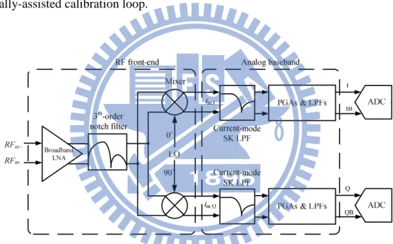
Figure 2-1 shows a direct-conversion RF receiver (DCR) for UWB. The receiver
includes an RF front-end (a low noise amplifier, a 3th-order notch filter and a
down-conversion mixer) and an analog baseband (PGAs and LPFs). The MB-OFDM
UWB signal is amplified and down-converted to the baseband with a bandwidth of
250 MHz. The strong out-of-band interferer is down-converted as well. To avoid
saturating the analog-to-digital converter (ADC) due to the interferer, the baseband is
required to pass signals and suppress interferers. As compared to narrowband systems,
design challenge of the UWB receiver lies in high linearity and wide bandwidth to
handle both signals and interferers.
Figure 2-1: Architecture of a direct-conversion RF receiver for UWB.
The performance of the UWB band group1 (3168~4752 MHz) may be degraded by
frequency bands of 5.15~5.25, 5.47~5.725, and 5.725~5.875 GHz. In Figure 2-2, if the
interferences are at 5.85 and 5.25 GHz, third-order inter-modulation (IM3) will be
generated at 4.5GHz and saturate in-band desired signal and also desensitize the
linearity. So the notch filter applied for the LNA is needed to reduce the interferences
at 5~6 GHz [17] [18]. There are several advantages and trade-offs between each notch
filter topology. Since the parasitic resistance of passive filter could not be canceled, the
Q- factor is worse than that of active notch filter. Second-order active topology has
better quality value, but some amount of wanted signal might be lost due to existing of
only one zero. Third-order active notch filter provides not only one zero but also one
pole that reduces the loss of gain of wanted signal [19]. Due to wide frequency range
of interferences, the notch filter must have frequency tuning and gm tuning functions.
If the interference could not be reduced enough, the gm tuning function can be turned
on to solve this problem. In this design, a wideband differential LNA with integrated
3th-order notch filter for interference rejection is designed.
Linearity restriction of the UWB RF receiver is at the output of the
down-conversion mixer (input of the analog baseband). Large signal swing at the
mixer output generates harmonics due to non-linearity of MOS transistors in the
switching cells of the mixer and the input stage of the analog baseband. One way to
reduce the signal swing without degrading SNR is to translate signals from the
voltage domain to the current domain. To do so, a voltage-mode OP Amp can be
configured as resistance feedback, forming low input impedance at the input of analog
baseband. In addition, a capacitor can be parallel-connected with the feedback resistor
to form a first-order low-pass filter to suppress out-of-band interferers. This method
has already adopted in narrowband receiver design to achieve high linearity under a
receiver, such as a UWB RF receiver. First of all, it requires realizing low input
impedance over the entire wide bandwidth. Second, we need current-mode filters.
Wideband current-mode circuits have been developed for applications of optical
wireline communications. Some design techniques can be borrowed here. For
example, the active feedback technique helps reduce input impedance of the
amplifiers. Also filters constructed by current-domain circuits have been developed.
Owing to WLAN 802.11a strong interferers are only 700 MHz away from
MB-OFDM UWB 4.5 GHz channel, single-pole filter provides insufficient roll-off at
700MHz away. The Sallen-Key filter has been applied to deeply filter specific
harmonics in some applications [21]. In this work, we realize a Sallen-Key filter
constructed by current-domain circuits to filter the strong interferers in current
domain efficiently.
Here, the reference specifications of the analog baseband are addressed following
to the receiver conformance requirement. The entire receiver must meet the required
sensitivity and signal-to-noise radio (SNR) of -80.8 dBm and 9.3 dB, respectively,
under the data rate of 53.3 Mb/s with the longest transmission distance of 10 m which
leads to the most strict sensitivity requirement to the receiver [2]. The maximum
received signal strength is -10 dBm. Hence, the dynamic range of the RF receiver is
70.8 dB. 10 dB of the required dynamic range is contributed by RF front-end, the
remainder is taken into account in the analog baseband. Owing to the full-scale of a
UWB ADC is -14 dBV (200 mVp), the required maximum voltage gain of the RF
receiver is 67.8 dB to amplify signals from the sensitivity level to the ADC full-scale
with a back-off of the MB-OFDM UWB signal peak-average radio (PAR) as 9 dB.
Given that the RF front-end voltage gain is fixed at 15 dB, the analog baseband shall
provide the maximum voltage gain of 52.8 dB. The required sensitivity translates to
nominal value of 4 dB. Consequently the required noise figure of the analog baseband
is less than 14 dB.
Linearity requirement for the RF receiver is constrained by the worst case that
strong out-of-band interferers at the 5 GHz band (WLAN 802.11a) cause serious SNR
degradation to the 4.5 GHz-channel as shown in Figure 2-2 [22]. The test case defines
two interferers allocated at 5.2 GHz and 5.85 GHz with the power level of -4 dBm.
The required sensitivity is -75 dBm and the required SNR remains 9.3 dB [23].
Assume the pre-filter in front of the RF receiver provides 25 dB attenuation for
out-of-band interferers. The required input-referred third-order intercept point (IIP3)
of the RF receiver is -1 dBm. In order to relax linearity requirement of the analog
baseband, assume a notch filter is designed with LNA and provides 20 dB attenuation
for out-of-band interferers. Therefore, the required out-of-band IIP3 of the analog
baseband shall be over -8 dBV at the maximum gain setting. The interferers at 5.2
GHz and 5.85 GHz also could cause second-order inter-modulation distortion. To
avoid degradation of SNR, the required IIP2 of the analog baseband should be better
than -5 dBV as 10 dB attenuation of interferers is provided by the first stage of the
analog baseband. According to the calculated specifications, Table I summarizes the
receiver requirements to comply MB-OFDM UWB performance.
Frequency 802.11a WLAN 4.75G Band group1 5.2~ 5.4 G IM3 of interferences 5.7~ 5.9 G 3.1G Band1 Band2 Band3
degradation at 4.5GHz channel.
TABLE I. Specifications of receiver
Overall receiver
Sensitivity -80.8 dBm
SNR 9.3 dB
Dynamic range 70.8 dB
Full-scale of a UWB ADC -14 dBV
Maximum gain 67.8 dB Attenuation of Pre-filter 25 dB IIP3 -1 dBm Noise figure 6.6 dB RF front-end Gain 15 dB
Attenuation of Notch Filter 20 dB
Noise figure 4 dB
Analog baseband
Bandwidth 250 MHz
Gain Range 61 dB
Maximum gain 53 dB
Gain control resolution 1 dB
Noise Figure 14 dB
Out-of-band IIP3 -8 dBV
Chapter 3
Architecture and Specifications of Transmitter
The architecture of the proposed transmitter is as shown in Figure 3-1, which carries
out the direct-conversion architecture, including an analog baseband, an IQ modulator,
a RF VGA, a D-to-S amplifier and a power amplifier. Moreover, a transmitted signal
strength indicator (TSSI) is also integrated. The analog baseband consists of a
5th-order Chebyshev low-pass filter and baseband VGAs. As the baseband signal input,
the low-pass filter eliminates the output harmonics from a digital-to-analog converter
(DAC). The baseband VGAs provide tunable attenuation from 9dB to 19dB to adjust
the signal amplitude to a pre-determined proper level for the IQ modulator. The IQ
modulator is designed to modulate baseband signals to RF frequency. A DC-offset
cancellation circuit is also integrated for improving the performance of carrier leakage
suppression. The RF VGA provides linear-in-dB gain tuning of 14dB. The D-to-S
amplifier is designed before the single-ended power amplifier for combining
differential signals with an acceptable gain and phase error from 3GHz to 8GHz.
Finally, the power amplifier is designed to boost the RF signals and linearly drive the
Figure 3-1: Block diagram of the wideband RF transmitter.
In digital baseband, DAC generates modulated signals with a sufficient
spurious-free dynamic range (SFDR) to meet the system requirement. Then an RF
transmitter performs I + j⋅Q to combine in-phase and quadrature-phase signals from the DAC and up-converts the modulated signals to the RF frequency. But the RF
transmitter introduces unwanted effect on the output signals such as carrier leakage,
sideband leakage and distortions simultaneously. The signal-to-noise ratio (SNR) is
the most important parameter to receiver design. However, the key parameter of
transmitter design is the signal-to-spur ratio (SSR). The carrier leakage, sideband
leakage and distortions all lead to SSR degradation.
According to the FCC regulation, the output power spectrum density of UWB is
limited to -41.3dBm/MHz. The maximum in-band signal power is calculated as
. 10 ) 528 ( 10 / 3 . 41 dBm Hz + ⋅LOG10 MHz =− dBm − (3.1)
The transmitter output power should be up to -7.5dBm assuming the signal
Listed in Table II is the transmitter link budget, which is a tradeoff between SSR and
linearity. The input voltage swing to this transmitter, or the output voltage swing from
a DAC, is assumed in the range from 125mVp to 375mVp for a flexible DAC interface.
For the optimal linearity performance of the IQ modulator, the input voltage swing at
the modulator input is fixed at 44.6mV (-27dBV). It requires gain tuning from -9dB to
-19dB in the analog baseband filter. Thus, it is specified a gain tuning range of 10dB
with the resolution of 1dB. The RF circuits following the analog baseband provide
9.5dB gain for the maximum output power of -7.5dBm.
Transmitter linearity is constrained by the signal peak-average ratio (PAR) of 9dB,
which leads to an instantaneous power increase of 9dB. Therefore, the RF transmitter
should have the ability to linearly transmit signals as large as +1.5dBm. Consequently
the required OP1dB is +1.5dBm. The carrier leakage emission is also strictly
regulated within -41.3dBm. Thus, the required carrier leakage suppression is derived
as . 3 . 31 ) 3 . 41 ( 10dBm − − dBm = dBc − (3.2) The leakage is lumped to the effect caused by DC offset. Since the voltage swing at
the IQ modulator input is 44.6mV (-27dBV), the input-referred DC-offset of the IQ
modulator should be less than 1.21mV (-58.3dBV). This small level requires a
DC-offset cancellation circuit. According to the transmit spectrum mask specified by
MB-OFDM UWB, the filter in the analog baseband should provide at least
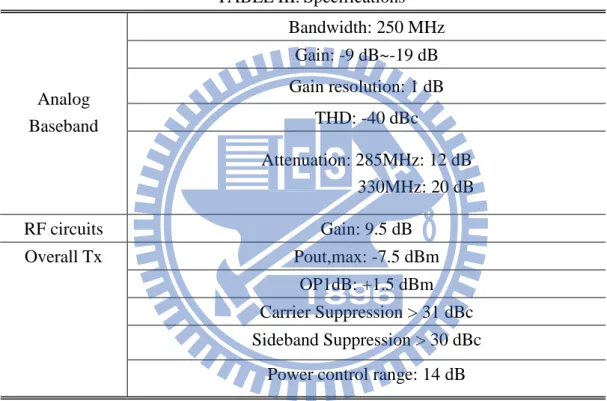
out-of-band attenuation of 12dB and 20dB at the frequencies of 285MHz and
330MHz, respectively. The design specification of the MB-OFDM UWB RF
TABLEII.Link budget of transmitter
DAC output swing 125 mVp -to- 375m Vp
(-18 dBV ~ -8.5 dBV)
Gain of analog filter -9 dB ~ -19 dB
Modulator input swing -27 dBV
Gain of RF stages 9.5 dB
Output power of transmitter -7.5 dBm
TABLEIII.Specifications Bandwidth: 250 MHz Gain: -9 dB~-19 dB Gain resolution: 1 dB THD: -40 dBc Analog Baseband Attenuation: 285MHz: 12 dB 330MHz: 20 dB RF circuits Gain: 9.5 dB Pout,max: -7.5 dBm OP1dB: +1.5 dBm Carrier Suppression > 31 dBc Sideband Suppression > 30 dBc Overall Tx
Chapter 4
Circuit Design of Receiver
4.1 RF Front-End
4.1.1 Low-Noise Amplifier (LNA)
The schematic of LC ladder LNA is shown in Figure 4-1. Gain switch function is
formed by the control bit (Gain_SW) that has 10dB gain difference between high and
low gain mode. Band control function is formed by the control bits LG (0~3) that
change equivalent capacitance of output load to switch to the desired UWB channel in
band group1 (3432, 3960 and 4488 MHz). In order to extend bandwidth at higher
frequency band, we shunt switch M5 and large resistor RL with the output loading LC
tank. If bandwidth is not enough at higher frequency band (512MHz), M5 can be
turned on by switch HF_ON to extend bandwidth, but it must sacrifice a little power
gain. The proposed notch filter was connected on the drain of M1 that provided low
impedance path for small signal current to ground at interference frequency. The ESD
protection circuit was added on the virtual ground position of input matching, so it
1 M 2 M 3 M 4 M L R out V ++++ 0 sw C 1 sw 2C 2 sw 4C 3 sw 8C 1 C 2 C L C 1 M 2 M 3 M 4 M L R 0 sw C 1 sw 2C 2 sw 4C 3 sw 8C 1 C 2 C HF _ ON dd V Gain _ SW dd V ====1.2V bias V ESD 2.5v LG0 LG1 S 2L 1 2L 5 M 5 M dd V Vdd L 2L Inv Notch Filter dd V Vdd L C
Output Buffer Output Buffer
B M MB B R RB out V −−−− in V ++++ Vin−−−− LG2 LG3 LG0 LG1 LG2 LG3
Figure 4-1: Schematic of LC ladder LNA core
4.1.2 Input Matching Analysis
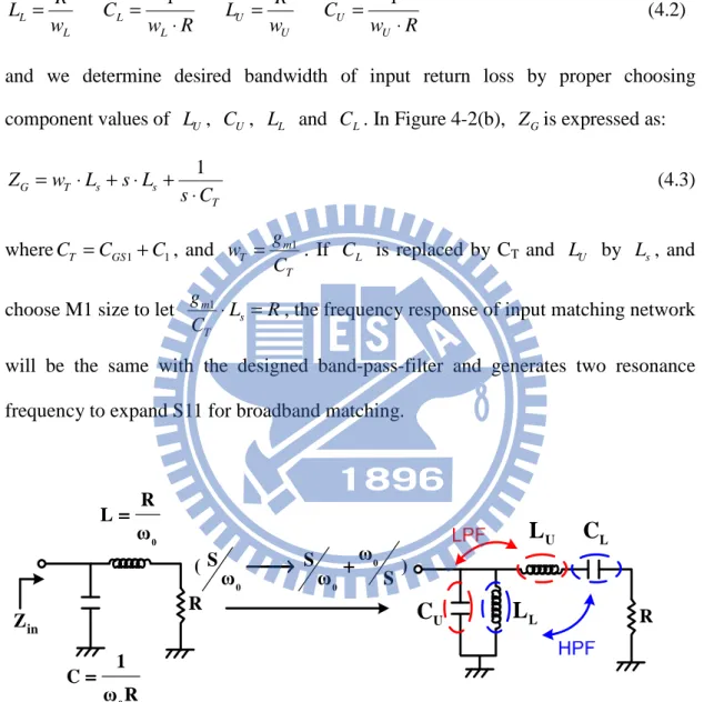
Consider two-order low-pass-filter as shown in Figure 4-2(a). Using the low-pass to
band-pass transformation, the shunt capacitor and series inductor can be transformed to
parallel LC and series LC network respectively. The two corner frequencies of
band-pass-filter are w andU w that define the fractional bandwidth (n) as [24]: L
L U L U w w w w n ⋅ − = (4.1)
Since n>1, the band-pass-filter can be viewed as a low-pass-filter combined with a
high-pass-filter. In this case, w is decided byU L ,U C and U w is decided by L L ,L C . L
The values of these components can be roughly expressed as:
R w C w R L R w C w R L U U U U L L L L ⋅ = = ⋅ = = 1 1 (4.2) and we determine desired bandwidth of input return loss by proper choosing
component values of L , U C , U LL and CL. In Figure 4-2(b), Z is expressed as: G
T s s T G C s L s L w Z ⋅ + ⋅ + ⋅ = 1 (4.3) whereCT =CGS1+C1, and T m T C g w = 1
. If CL is replaced by CT and L by U L , and s
choose M1 size to let L R C
g
s T m1⋅ =
, the frequency response of input matching network
will be the same with the designed band-pass-filter and generates two resonance
frequency to expand S11 for broadband matching.
0 1 C ω R ==== R 0 R L ω ==== in Z R 0 0 0 ω S S ( ) ω
→
→
→
→
ω ++++ S LC
UC
L
L UL
S T ω L (R) GS1 1 L C C (C ) ++++ 2 U C (C ) 1 L L (L ) S U L (L ) S L 1 C G Z 1 M
(b) Schematic of the LNA input matching network
Figure 4-2(b): Design method analysis for input matching of the LNA core.
4.1.3 Gain analysis
The small signal model of high gain mode is shown in Figure 4-3(a), the voltage gain
can be derived by solving the trans-impedance and neglecting effects of output buffer.
Overall voltage gain can be calculated as:
eq L L T s s m m in out C L s L s C L s L g s g v v ⋅ ⋅ + ⋅ ⋅ ⋅ ⋅ + ⋅ ⋅ + − = 2 2 1 1 1 1 (4.4)
where Ceq is the total capacitance at output node that including parasitic capacitor
db
C of the cascode stage (M3 and M4) and capacitor array value which controlled by
LG (0~3). From equation (4-4), If C decreases, the voltage gain increases and eq
desired band will “move” to higher frequency.
When switch to low gain mode as shown in Figure 4-3(b), M2 off and M3 on. If
sizes of M2 and M3 are identical, the small signal current that flows into the drain of
M1 is equal to that in high gain mode, so input frequency response (S11) will be the
load will be 1/3 times of that flows into the drain of M1 (i.e. gm1⋅VGS1 =3⋅gm4⋅VGS4), so the overall voltage gain of low gain mode will be reduced by 3 times compared
with high gain mode. That means the power gain (S21) of low gain path is 9.54
(20⋅log103) dB less than that of high gain mode.
T
C
V
GS++++
−−−−
LC
LL
C
eq. m1 GSg V
SL
ideal cascode
GZ
GV
I
G outZ
outV
TC
V
GS++++
−−−−
LC
LL
C
eq. m1 GS1g V
SL
GZ
GV
I
G outZ
outV
m4 GS4g
V
m3 GS3g
V
(a) High gain mode model (b) Low gain mode model
Figure 4-3: Small signal model analysis for LC ladder LNA.
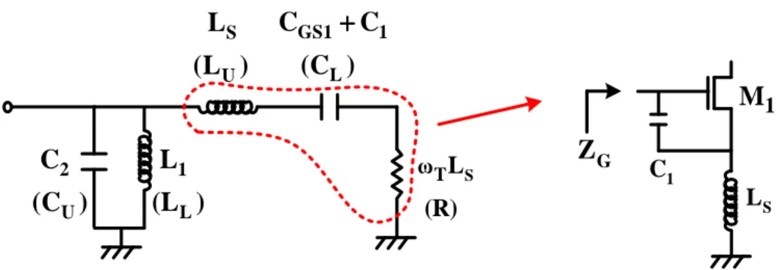
4.1.4 Third-Order Notch Filter Design
Third-order active notch filter is the best topology to reject interferences due to deep
and steep notch at resonance frequency. It needs 2 series inductors for differential
LNA and occupies large chip area. The circuit topology of proposed third-order active
notch filter is shown in Figure 4-4 that only needs one center-taped parallel inductor to
save chip area for differential topology. The input impedance from M1 gate can be
T x T f gs m g in C jw R C jw C C w g r Z ⋅ + = ⋅ + ⋅ ⋅ − =( 2 1 ) 1 1 1 ' (4.5) where f gs f gs T C C C C C + − = and f gs m g x C C w g r R ⋅ ⋅ − = 2 1
1 .SoZ can be equivalent to the RLC in
network as shown in Figure 4-5. Total equivalent parallel parasitic resistance RP can be
expressed as:
(
)
(
)
(
)
(
f T)
Lf x f T x Lf f x Lf T f PC PL p R C L w R L w C w R R L w R R C L R R R + ⋅ ⋅ ⋅ ⋅ = ⋅ ⋅ + ⋅ ⋅ ⋅ = = 2⋅ 2 2 2 2 2 1 1 // (4.6)If RP approaches to infinity, the condition of the best Q-factor of the filter occurs as
shown in equation (4.7):
(
)
gs f m g T f Lf C C w g r C L w R ⋅ ⋅ = + ⋅ ⋅ 2 1 1 2 2 (4.7)The power gain of LNA at interference frequency(w) will lower to minimum as the
sizes of transistor M1 and other passive elements satisfy equation (4-7), then Q-factor
of this 3-order active filter will be maximize at the interference frequency. As the
condition occurs, Z can be expressed as: in
(
)
(
f T)
T f f T in C L s C s C C L s L s C s C s Z ⋅ ⋅ + ⋅ ⋅ + ⋅ ⋅ + = ⋅ ⋅ + ⋅ = 2 1 1 2 1 1 1 // 1 1 (4.8)Equation (4.8) generates not only one zero but also one pole. The resonant frequency
of pole is T f wanted C L f ⋅ ⋅ = π 2 1
, and resonant frequency of zero
is
(
T)
f wanted C C L f + ⋅ ⋅ = 1 2 1π . Figure 4-6 is the schematic of proposed 3-order active
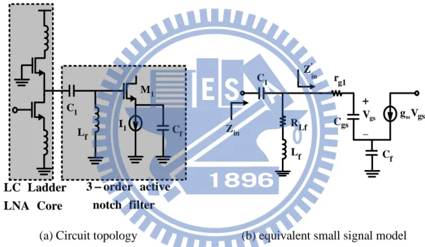
tuning function to track different positions of interferences. Zero resonant frequency
fint can be varied by CT. Thus, varactor C3,4 and C6 are added to vary equivalent
capacitor of Cgs and Cf respectively and controlled by 3-bits control (F_Tune). Since
equivalent values of Cgs and Cf are varied, equation (4.7) is difficult to satisfy at fixed
trans-conductance of M1 (g ). The switch transistors Pm1 0~P3 provide different current
for M1 to changeg to satisfy equation (4.7) and compensate Q-factor of the notch m1
filter. If gain attenuation is not enough at interference frequency, the gm1tuning
circuit can be turn on to achieve enough high Q-factor.
f C f L 1 M f L Lf R g1 r gs C Vgs _ ++++ f C m gs g V 1 I 1 C 1 C in Z in ' Z 3 order active notch filter −−−− LC Ladder LNA Core
(a) Circuit topology (b) equivalent small signal model
Figure 4-4: Proposed 3-order active notch filter (half-circuit)
f L 1 C in Z Rx T C Lf R 1 C in Z Lf CT P PL// PC R R R ====
1 M dd V F _ Tune F _ Tune F _ Tune 1 C 2 C 0 M 3,4 C 5 C 6 C f L Q _ Tune0 Q _ Tune1 Q _ Tune2 Q _ Tune3 gs C f C 0 P P1 P2 P3 NF _ in p0 I Ip1 Ip 2 Ip 3 dd V dd V Vdd m1 g tuning circuit + ++ + −−−−
Figure 4-6: Schematic of third-order active notch filter.
4.2 Analog Baseband
As shown in Figure 4-7, a proposed wideband, wide dynamic range baseband chain is
composed in the order of three-stage current-mode PGAs, a Gm-C filter, three-stage
current-mode PGAs, an I-to-V converter and a voltage buffer. Besides, a
digital-assisted DC-offset calibration loop is adopted to eliminate DC-offset of the
baseband chain. The current-mode PGA is realized by balanced current-mode
amplifiers to provide gain and gain tuning range. The first current-mode PGA also
includes a current-mode SK LPF. Placed in the middle of the baseband chain, the
Gm-C filter filters out-of-band unwanted signals. The I-to-V converter is used to covert
Finally, a voltage buffer is designed for driving analog-to-digital converter (ADC). Buffer … … Buffer Gm-C Filter I-to-V DC-offset Calibration loop Gm-C Filter SAR Digital Control Logic 1-bit Quantizer I-to-V In-phase Quadrature-phase DAC 8-bits DAC 8-bits Current-mode SK LPF Current-mode SK LPF Current-mode PGA Current-mode PGA DAC 8-bits DAC 8-bits Current-mode PGAs Current-mode PGAs Current-mode PGA Current-mode PGAs Current-mode PGAs Current-mode PGAs DAC 8-bits DAC 8-bits DAC 8-bits DAC 8-bits DAC 8-bits DAC 8-bits 64-bits 64-bits DAC 8-bits DAC 8-bits DAC 8-bits DAC 8-bits DAC 8-bits DAC 8-bits iin+I iin -I iin + Q iin -Q Vout+ I Vout -I Vout+Q Vout -Q
Figure 4-7: Block diagram of the wideband, wide dynamic range baseband chain.
In [11], the gain tuning function of the UWB low-pass filter is attained by
controlling trans-conductance (gm) in the filter circuits, resulting in less gain, less gain
tuning range and poor noise figure performance. In this design, the gain tuning
function of the analog baseband is accomplished by the current-mode PGAs. The
three-stage current-mode PGAs in front of the Gm-C filter are designed with the gain
of 47 dB to suppress Gm-C filter noise. So the analog baseband exhibits much better
noise figure performance than that reported in [11]. The three-stage current-mode
PGAs follow the Gm-C filter to achieve the required overall gain and dynamic range.
The analog baseband has gain tuning range from -9 dB to 73 dB, which leads to
maximum gain of 73 dB and the dynamic range of 82 dB with gain resolution of 0.5
dB. The corner frequency of the baseband chain, determined by the Gm-C filter and
adjusted by the capacitors arrays, ranges from 250 MHz to 300 MHz. A Gm-C
variation.
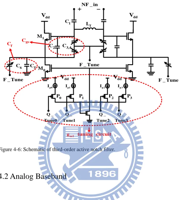
4.2.1 Programmable gain Amplifiers (PGAs)
Ideally the current amplifier should have infinite output impedance and zero input
impedance for optimal current signal transfer. But in the advance CMOS process,
drain-source (Rds) resistance is greatly decreased. Cascode topology for increasing
output impedance cannot be easily realized due to the headroom limitation under a
low supply voltage. Circuit design effort is therefore on very low input impedance.
PGAs are constructed by the current amplifier in the simple common-gate (CG)
configuration, as shown in Figure 4-8(a), exhibiting an input resistance of 1/ gm1. Low
input impedance indicates a large-size transistor and high bias current, and in turn,
leads to large input capacitance and high input-referred noise from the tail current
source [25]. As shown in Figure 4-8(b), a series-series feedback loop through M3 and
M4 is added to decrease the input resistance without degrading bandwidth and noise
performance. The input impedance of the current amplifier with the feedback is
derived as ) ( ) ( ) ( ) ( 1 2 4 3 1 2 4 1 4 2 2 1 4 2 2 1 1 2 1 2 1 2 1 3 3 1 2 4 4 2 2 1 2 1 2 1 m m m m m m m in m m m m m in m in m m m m m m m in g g g g g g g C g C g C s g C g C g C C C s g C C C s g g g g g C g C s C C s g Z ⋅ + − + + + + + + ⋅ ⋅ ⋅ − ⋅ + + + ⋅ = (4.8)
where C1 =Cgs4 +Cds4 +Cds3, C2 =Cgs2 +Cds2 +Cgs3. At low frequencies, the input resistance is reduced to ) 1 ( 1 2 3 4 1 1 , m m m m m DC in g g g g g Z = ⋅ − ⋅ (4.9)
The input-impedance is reduced by a factor of 1−gm1⋅gm3/
(
gm4⋅gm2)
due to the series-series feedback. If PMOS is used in M4, higher feedback gain can be found,but the bandwidth of the current amplifier will be reduced.
Figure 4-8: (a) Conventional CG current amplifier, (b) Proposed current amplifier with series-series feedback.
The complete schematic of the differential PGA is shown in Figure 4-9. The input
stage is accomplished by the series-series feedback for low input impedance. The
bandwidth of the feedback must be large enough across the entire channel band (250
MHz in this case since direct conversion is used). As shown in Figure 4-10, the
simulated input impedance exhibits a low value of 15 ohm up to 1 GHz. The PGA
load is composed of current mirrors in the cascode configuration for high output
impedance. Current gain is programmable by changing the size ratio of the current
mirror load using switches to turn on or off the cascode stage. Therefore, current
consumption of the PGA is proportional to its gain. For linearity concern, DC bias
current is designed in class-A operation. As to the output DC voltage, it is defined by
a common-mode feedback (CMFB) amplifier and matched to the input DC voltage of
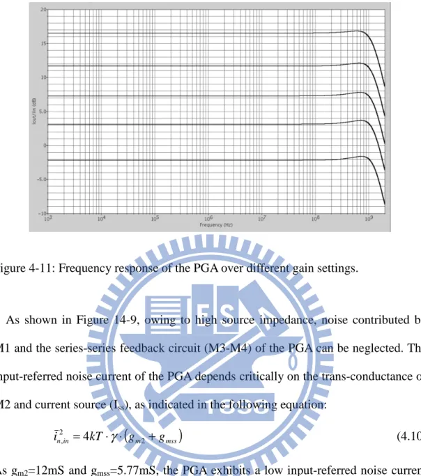
the next PGA stage. Figure 4-11 shows the frequency response of the PGA over
Figure 4-9: The schematic of PGA based on current amplifier.
Figure 4-11: Frequency response of the PGA over different gain settings.
As shown in Figure 14-9, owing to high source impedance, noise contributed by
M1 and the series-series feedback circuit (M3-M4) of the PGA can be neglected. The
input-referred noise current of the PGA depends critically on the trans-conductance of
M2 and current source (Iss), as indicated in the following equation:
inin = kT⋅ ⋅
(
gm2+gmss)
2
, 4 γ (4.10) As gm2=12mS and gmss=5.77mS, the PGA exhibits a low input-referred noise current
of 42.5 pA/ √ Hz. Simulated by SpectreRF, noise analysis shows that the
input-referred noise of the analog baseband is dominated by the current noise of the
first two PGAs and governed by (4.10). Circuit noise after the first two PGAs is
greatly suppressed by the high gain of the first two PGAs.
In the first stage of the PGAs, the current-mode SK LPF is implemented for
filtering the interferers from WLAN 802.11a signals [26-27]. The schematic is similar
to the current amplifier except the resistor-capacitor feedback at the output as shown
reduced, which leads to relaxed linearity requirement to the following PGAs. The
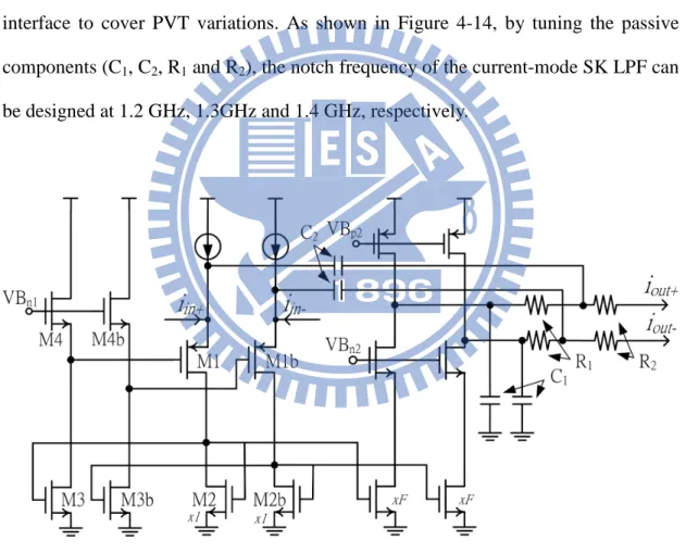
equivalent circuit model of the current-mode SK LPF is shown in Figure 4-13. The
transfer function of the current gain can be derived as
( )
( )
( )
[
(
)
]
{
(
)
[
(
)
]
}
1 1 ) ( 1 2 1 1 2 2 2 2 1 2 1 2 2 1 2 1 2 + + + + + + + + − + = = F R R C R R C s R R r R R C C s F r sC r R C C s s i s i s H i i i i in out (4.11)where F is the current gain of the current amplifier and ri is the non-zero input
resistance of the current amplifier. Composed by a complex-conjugate pair, the zeros
in equation (4.11) form a transmission zero and make a notch in the frequency
response. By assuming that the zeros are located ats=−a± jb, we can write the numerator of (4.11) in the form of
(
2 2)
2 2 ) (s s as a b Hnum = + + + (4.12) The notch frequency (wt) satisfies the following equation:( )
(
)
0 = =wt s num ds s H d (4.13)Substituting (4.12) into (4.13), we obtain the notch frequency as:
2 2
a b
wt = − (4.14) AssumeC1 =C, C2 =αC, R1 =R, R2 =λR, ri =βR and F=-1. (4.11) can be rewrote as follows:
( )
( )
( )
(
)
( )
(
)
(
)( )
2 2 2 2 1 1 s 1 1 s RC s RC s RC s i s i s H in out βλ β λ α βλ β λ α αβ λ αβ βλ β λ α αβ + + + + + + + + + + × + + = = (4.15)Solving a and b by using (4.12) and numerator of (4.15), notch frequency (wt) and
follows: 2 1 1 1 − = αβ RC wt (4.16) αβ 1 = z Q (4.17)
Besides, pole frequency (wp) and quality factor (Qp) of the denominator of (4.15) can
be derived as follows:
(
λ β βλ)
α + + = 1 1 RC wp (4.18)(
)
αβ λ βλ β λ α + + + + = 1 p Q (4.19)Finally, we can obtain the filter parameters (RC, α , β and λ) by solving (4.16), (4.17), (4.18) and (4.19).
Consider the worst case that the UWB channel of band 3 (frequency centered at 4.5
GHz) is used. The WLAN 802.11a interferer in the RF band of 5.7 GHz~5.9 GHz will
be down-converted to the baseband frequency of 1.2 GHz~1.4 GHz. The notch can be
designed in the frequency of 1.2 GHz~1.4 GHz to filter the interference signals.
Actually another WLAN 802.11a interfere in the RF band of 5.2 GHz~5.4 GHz is
down-converted to the baseband frequency of 0.7~0.9 GHz, closer to the signal band.
Yet choosing the notch in 1.2~1.4 GHz causes less in-band signal degradation while
reducing the same amount of baseband inter-modulation distortion due to these two
interferers. Therefore, the inter-modulation term falls into band 3 caused by WLAN
802.11a signals in 5.2 GHz~5.4 GHz and in 5.7 GHz~5.9 GHz can be greatly reduced.
Thus, we design the notch frequency (Wt) of the current-mode SK LPF at 1.3 GHz
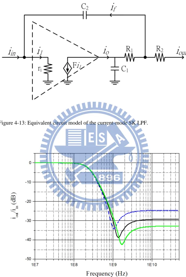
Assume C1 is 1 pF, we can have the following filter parameters from (4.16~4.19): 0637 . 2 = α 0.0538 = β 1.4116 = λ -10 10 3.5693 RC= ×
The simulated frequency response of the current-mode SK LPF is shown in Figure
4-14. In the circuit design, the capacitors (C1 and C2) and resistors (R1 and R2) in the
SK LPF are designed in a binary-weighted array and can be tuned by a 3-wire control
interface to cover PVT variations. As shown in Figure 4-14, by tuning the passive
components (C1, C2, R1 and R2), the notch frequency of the current-mode SK LPF can
be designed at 1.2 GHz, 1.3GHz and 1.4 GHz, respectively.
Figure 4-13: Equivalent circuit model of the current-mode SK LPF.
4.2.2 G
m-C filter
The Gm-C filter utilizes the LC ladder structure to accomplish the 6th-order Chebyshev
low-pass filter as shown in Figure 4-15. The schematic of the Gm cell is as shown in
Figure 4-16. The super source follower structure as in [28] is applied to improve the
linearity of the Gm cells. Regulated by the gain-bandwidth product limit, the Gm-C
filter is therefore designed with no gain to extend its bandwidth to 250 MHz. However,
the PVT process variation might cause bandwidth change significantly. Gm-C
calibration circuit is necessary to reduce impact on the cutoff frequency of the channel
selection filter.
Figure 4-16: The schematic of Gm cell in Gm-C filter.
Calibration circuits are integrated to tune the capacitors arrays against the variation.
The main issue is accurate implementation of the time constant (Gm/C). In [29], the
time constant is tuned automatically by varying Gm. The analog-type tuning method is
sensitive to noise and consumes much power. Instead, digital-type control of passive
component C is chosen.
Figure 4-17 shows the architecture of the Gm-C calibration loop adopted in this
design. The Gm-C calibration loop consists of a Gm cell, a capacitor array, a
comparator and a digital controller. The Gm cell and the capacitor array are identically
matched to those used in the filter chain. An accurate reference clock signal is used to
control a MOS switch between DC voltage source (V2) and the Gm cell output to
decide the charging time of the capacitor array. The Gm cell output voltage (V(t)) is
compared to a reference voltage (Vref) corresponding to the desired Gm/C time
constant. By the algorithm of successive approximation (SAR) search, the digital
time domain is governed by (1 2) 1 2 0 ( ) m t t g V V C V t e dt V − − =
∫
+ . (4.20) Figure 4-18 shows an example of the timing diagram of CLK, CLKz and V(t) duringthe calibration. Initially, the capacitor array is set as <1 0 0 0> , CLK is high, and V(t)
is charged to V2. When CLK becomes low, V(t) is further charged with the time
constant of Gm/C as indicated in (4.20). If C is too small, V(t) is eventually higher
than Vref as CLK turns from low to high, or vice versa. It takes four clock cycles for
the digital controller to process SAR search to set the capacitor array to the
appropriate result. Consequently, the capacitor array is calibrated to achieve the
desired Gm/C time constant.
Figure 4-18: Timing diagram of Gm–C calibration.
4.2.3 DC-Offset Calibration
The issues of balanced current amplifiers are poor IP2 performance owing to
DC-offset in the circuits. As shown in Figure 4-19, a typical balanced current
amplifier is with an input-referred DC-offset current, Ioffset. Therefore, the received
input currents iin+ and iin− to the amplifier can be described as
) 180 cos( ), cos( = ⋅ + o ⋅ + = − + I A wt i A wt iin offset in (4.21)
Circuit non-linearity will lead to output current, iout as
... 3 2 + ⋅ + ⋅ + ⋅ + = in in in out a b i c i d i i (4.22)
The balanced output of the current amplifier can be derived as
... )) 2 cos( 1 ( 3 ... ⋅ ⋅ ⋅ 2 ⋅ + + = − − + i d I A wt
iout out offset (4.23)
It indicates that DC-offset current results in the second-order distortion at the output
Another second-order linearity issue is poor IP2 performance due to absence of
common current biasing for the balanced branches in typical circuit implementation.
In [30], a digital calibration scheme had been proposed for calibrating IIP2 of a
down-conversion mixer. Here, the critical second-order distortion issue in the analog
baseband is tackled by using a digitally-assisted DC-offset calibration. The digital
technique benefits in circuits and substrate noise immunity, low power consumption
and fast settling time.
Figure 4-19: A typical balanced current amplifier with an input referred DC-offset current.
As shown in Figure 4-7, the digitally-assisted DC-offset calibration consists of a
1-bit quantizer, one digital control logic unit and digital-to-analog converters (DACs).
DC-offset current in the current-mode PGA is converted to DC-offset voltage at the
PGA output by the equivalent output resistance. Therefore, DC-offset of balanced
branches in the PGA can be sensed by a voltage-mode 1-bit quantizer as shown in
Figure 4-20. The 1-bit quantizer is composed of an auto-zeroing amplifier and a latch.
then amplifies the DC-offset of balanced branches in another half of a clock period.
The latch converts the output of the auto-zeroing amplifier into a 1-bit digital code. To
save the time consumed by the DC-offset calibration, the auto-zeroing amplifier and
the latch work as a pipeline in time domain. That is, as the latch works, the
auto-zeroing amplifier performs self DC-offset elimination to prepare for sampling
next incoming DC-offset.
(a)
(b)