A Novel Generalized Zero Vector Control Circuit for High Efficiency Three-phase Inverter
Tsung-Cheng Chen, Gwo-Jen Chiou, Jeng-Yue Chen and Cyuan-Jyun Chen
Department of Electrical Engineering, National Formosa University No.64, Wunhua Rd., Huwei Township,
Yunlin, Taiwan, R. O. C. 632
E-mail of Corresponding Author: [email protected] Telephone: +886-5-6315607
Abstract — In this paper, based on generalized zero vector a novel simple PWM control circuit for a three-phase inverter is presented. The proposed control circuit, consists of a simple analog circuit to achieve function of DPWM (Discontinuous Pulse Width Modulation), has several advantages such as lower switching losses, higher efficiency and voltage usage utility, pure sinusoidal output and cost down etc. In practical, based on conventional SPWM the proposed control circuit, without complicated calculation, can generate the modulation signals of DPWM to drive an inverter with high efficiency. Finally, some experimental results are presented for verification.
Keywords : generalized zero vector, switching losses, DPWM
I. INTRODUCTION
Variable voltage and variable frequency three-phase AC sources are widely used in industrial military and many general applications. There are many methods to achieve a variable voltage and variable frequency three-phase AC source.
With the advent and wide acceptance of the high power switching devices such as GTOs, IGBTs and MOSFETs, the switching behavior of converter has been improved to a great extent. Consequently, the research interests in the area of static converters have now been shifting forward improving the efficiency of conversion [1].
Now the SVPWM is widely used in three-phase inverter due to lower switching loss and higher voltage usage [2-3]. To improve the disadvantage of SVPWM, such as complicated calculation, harmonic injection PWM are presented [4-7]. The magnitude of injection harmonics is also needed to decide.
Therefore, in three-phase inverter has not idea drive method in PWM modulation.
In this paper, the generalized zero vector control is presented. To simplify the control circuit, without changing SPWM control circuit, a generalized zero vector controller is cascaded in SPWM control loop. The advantages of the proposed control, such as lower switching loss, higher voltage usage and simple control circuit etc., are achieved. Next, the detail of the proposed controller is described as follows.
II. GENERALIZEDZEROVECTORCONTROLOF THREE-PHASEINVERTER
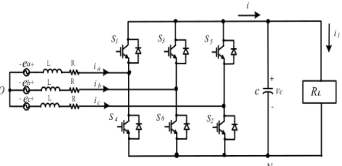
The main circuit of the three-phase AC/DC converter is shown in Fig. 1. Basically, the proposed converter consists of six switches in series with three boost type inductors and a capacitor. The six switches also include their body diodes to achieve bidirectional power flow capability. A typical gating signal is shown in Fig. 2 for reference. It is seen that each arm of the bridges can be controlled separately. Hence, the state equation can be derived by state-space averaging technique [8- 9] as follows:
NO a
a
L t
c t c t b t a
e V e e i i i
d R d d
d R
d R
d R
d dV
d di d di d di
c L L L
⎥⎥
⎥⎥
⎦
⎤
⎢⎢
⎢⎢
⎣
⎡
−
⎥⎥
⎥⎥
⎦
⎤
⎢⎢
⎢⎢
⎣
⎡ +
⎥⎥
⎥⎥
⎦
⎤
⎢⎢
⎢⎢
⎣
⎡
⎥⎥
⎥⎥
⎥⎥
⎦
⎤
⎢⎢
⎢⎢
⎢⎢
⎣
⎡
−
−
−
−
−
−
−
=
⎥⎥
⎥⎥
⎥⎥
⎥⎥
⎥
⎦
⎤
⎢⎢
⎢⎢
⎢⎢
⎢⎢
⎢
⎣
⎡
⎥⎥
⎥⎥
⎦
⎤
⎢⎢
⎢⎢
⎣
⎡
0 1 1 1
0 1 V
0 0
0 0
0 0
0 0 0
0 0 0
0 0 0
0 0 0
c b
c c b
3 2 1
3 2
1 (1)
Where d1, d2 and d3 are duty ratios of switch S1, S3
and S5, respectively. The ESR of the capacitor is neglected without significant influence, and
L:inductance C:capacitance
R:series resistance of inductor L
RL:load resistor
Assume that ia +ib +ic =0 and ea +eb +ec =0, then from Eq. (1), one can get
c K
K
NO d
V ⎟ν
⎠
⎜ ⎞
⎝
− ⎛
=
∑
= 3
3 1
1 (2)
N S3
Vc L +
- S2
S1
S4
S
S
5
6 - +
- + - +
L L
R R L R
O
il
ia ib ic
i
ea eb
ec c R
Fig. 1 Circuit of the three-phase AC/DC converter
t
t
t
t t 0 t
0 0 0 0
0 S1
S2
S3
S4
S6
S5
TS
d ′1
TS
TS
d ′2
TS
d ′3
Fig. 2 A typical gating signals of switch
Then, substituting Eq.(2) into Eq.(1) one has a complete state space averaged model as follows :
⎥⎥
⎥
⎦
⎤
⎢⎢
⎢
⎣
⎡
⎥⎥
⎥⎥
⎥⎥
⎦
⎤
⎢⎢
⎢⎢
⎢⎢
⎣
⎡
−
−
−
−
−
−
=
⎥⎥
⎥
⎦
⎤
⎢⎢
⎢
⎣
⎡
′
′
′
3 2 1
c b
3 2 3 1 3
1 3
1 3 2 3
1 3
1 3 1 3 2 1
d d d
e e e V
a
C
(3)
Where
(ω +φ)
= +
−
′ = Ri V t
d L di e
e a m
t a a
a sin (4)
(
1200)
sin + −
= +
−
′ =e L did Ri V ωt φ
e b m
t b b
b (5)
(
1200)
sin + +
= +
−
′= Ri V ωt φ
d L di e
e c m
t c c
c (6)
1
0≤dk, k=1,2,3≤ (7)
Using the generalized zero vector control and assuming
1=0
d , from Eq. (3) the d and 2 d can be obtained as 3 follows :
c a
b e
d e ν
′
−
= ′
2 ,
c a
c e
d e ν
− ′
= ′
3 (8) Similarly, the other results are also listed in Table I.
Where
vVcm dm 3
= , α = tω +φ (9) Table I The duty cycle by generalized zero vector control
1 =0
d d1 =1
d2 −dmcos
(
α−600)
1−dmcos(
α −600)
d3 −dmcos
(
α −1200)
1−dmcos(
α −1200)
Period 1
2 =0
d d2 =1
d1 −dmcos
(
α +1200)
1−dmcos(
α +1200)
d3 −dmcos
(
α +1800)
1−dmcos(
α +1800)
Period 2
3 =0
d d3 =1
d1 −dmcos
(
α +600)
1−dmcos(
α +600)
d2 −dmcos
( )
α 1−dmcos( )
αPeriod 3
In order to satisfy 0≤dk, k=1,2,3≤1, there are three periods in one cycle. Hence, from Table I the desired duty cycle dk*, k=1,2,3 are presented in Fig. 3 and Fig. 4.
Fig. 3 The desired duty cycle dk*, k=1,2,3when dk, k=1,2,3=0, respectively
Fig. 4 The desired duty cycle dk*, k=1,2,3when dk, k=1,2,3=1, respectively
We can find the one bridge of inverter is not switching.
The number of switching can be reduced one-third. Hence, the lower switching loss can be achieved. In addition, compared with sine PWM, from Table I the voltage utility also can be increased ,i.e., 115%.
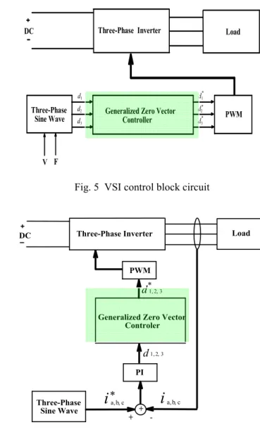
III. THECONTROLSTRATEGIESOFVSIANDCSI Applied generalized zero vector controller in VSI and CSI inverter, the control circuits are presented in Fig. 5 and Fig. 6, respectively.
From Fig. 5 and Fig. 6, one can find the simple control
circuit is cascaded in SPWM control. Basically, the waveforms of duty cycle which is generated from SPWM can be rearranged by the proposed generalized zero vector controller. Hence, without complicated calculation the proposed controller has lower switching loss and higher voltage utility than SPWM. Next some experimental results are presented as follows.
DC
V Three-Phase PWM Sine Wave
Three-Phase Inverter Load
Generalized Zero Vector Controller
F d1
d2
d3
d1
d2
d3
*
*
*
Fig. 5 VSI control block circuit
+ +
- DC
PWM
Three-Phase Inverter Load
Generalized Zero Vector Controler
PI
Three-Phase Sine Wave
c , b ,
i
a c, b ,
i
*a3 , 2 ,
d*1
3 , 2 ,
d1
Fig. 6 CSI control block circuit
IV. SOMEEXPERIMENTALRESULTS
First, the generalized zero vector controller is applied to VSI inverter. The one phase waveform of duty cycle by generalized zero vector control is shown in Fig. 7. The steady state output waveform of one phase current is presented in Fig.
8. In Fig. 8, the amplitude of output current is 1.5A. In Fig. 9, the output current is changed from 0.75A to 1.5A and the output frequency is also change from 30Hz to 60Hz. The output current has very fast response as shown in Fig. 9.
Similarly, the output current of CSI is shown in Fig. 10 and Fig. 11. In Fig. 11, the output current is also has nice response.
Therefore, the proposed generalized zero vector controller indeed has very nice performance.
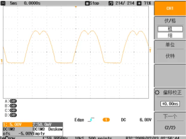
Fig. 7 Waveform of the desired a-phase duty cycle
(5V/div, 5ms/div)
Fig. 8 Steady-state current waveform of VSI
(1A/div, 5ms/div)
Fig. 9 Transient current waveform of VSI (0.75A → 1.5A, 30Hz→60Hz)
(5V/div, 5ms/div)
Fig. 10 Steady-state current waveform of CSI
(5V/div, 5ms/div)
Fig. 11 Transient current waveform of CSI (0.2A → 1A, 30Hz→60Hz)
(5V/div, 5ms/div)
V. CONCLUSIONS
In this paper, based on generalized zero vector a novel simple PWM control circuit for three-phase inverter is presented. The proposed control circuit has several advantages such as lower switching losses, higher efficiency and voltage usage utility, pure sinusoidal output and cost down etc.. In practical, based on conventional SPWM the proposed control circuit, without complicated calculation, can generate the modulation signals of DPWM to drive an inverter with high efficiency. Finally, from experimental results the proposed controller has nice performance and can be easily applied to any type inverter or converter.
REFERENCES
[1] Muhammad H. Rashid, "Power Electronics: Circuits, Devices, and Applications", Prentice-Hall, Inc., 1993.
[2] Van der Broeck H.W., Skudelny H.-C. and Stanke G.V., "Analysis and realization of a pulsewidth modulator based on voltage space vectors",
Industry Applications, IEEE Transactions on Volume 24, Issue 1, Part 1, Jan.-Feb. 1988, pp.142-150.
[3] Xiaoling Wen and Xianggen Yin, "The SVPWM fast algorithm for three-phase inverters", Power Engineering Conference, 2007. IPEC 2007. International, 3-6 Dec.2007, pp.1043-1047 .
[4] Hava A.M., Kerkman R.J. and Lipo T.A., "A high performance generalized discontinuous PWM algorithm", Applied Power Electronics Conference and Exposition, 1997. APEC '97 Conference Proceedings 1997., Twelfth Annual Volume 2, 23-27 Feb. 1997 pp.886-894.
[5] A. M. Hava, R. J. Kerkman, and T. A. Lipo, “Carrier-based PWMVSI overmodulation strategies: analysis, comparison, and design,”IEEE Trans. Power Electron., vol. 13, pp. 674-689, July 1998.
[6] A. M. Hava, R. J. Kerkman, and T. A. Lipo, "Simple analytical and graphical methods for carrier based PWM-VSI drives," IEEE Trans.
Power Electron., vol. 14, pp. 49-61, January 1999.
[7] J. A. Houldsworth and D. A. Grant, “The use of harmonic distortion to increase the output voltage of a three-phase PWM inverter,” IEEE Trans. on Industry Applications, pp.1224–1228, September/October 1984.
[8] T.C. Chen, "New AC/AC converters and applications to induction motor drives," National Tsing Hua University Doctoral dissertation, 1993.
[9] J.Y. Chen, "High Performance Active Three-Phase Boostbuck Rectifier," National Tsing Hua University Doctoral dissertation, 2001.
[10] Jilei Gao, Jianqiang Liu, Zhongping Yang and Zheng T.Q., "A Novel DSP Based Space Vector PWM Switching Pattern for Current-Source Converters", IEEE Conference, 3-5 June 2008, pp.902-907.