行政院國家科學委員會專題研究計畫 成果報告
利用 Z-轉換技術設計及製作嵌入微波濾波器之微波放大器 (第 3 年)
研究成果報告(完整版)
計 畫 類 別 : 個別型
計 畫 編 號 : NSC 97-2221-E-011-023-MY3
執 行 期 間 : 99 年 08 月 01 日至 100 年 07 月 31 日 執 行 單 位 : 國立臺灣科技大學電子工程系
計 畫 主 持 人 : 徐敬文
計畫參與人員: 碩士班研究生-兼任助理人員:黃瀚平 碩士班研究生-兼任助理人員:戴維志 碩士班研究生-兼任助理人員:吳育智 博士班研究生-兼任助理人員:張育維
公 開 資 訊 : 本計畫涉及專利或其他智慧財產權,2 年後可公開查詢
中 華 民 國 100 年 12 月 03 日
中 文 摘 要 : 本計畫提出嵌入式帶通濾波器的超寬頻功率放大器之設計。
採用離散時域的概念,將砷化鉀場效應電晶體之 S 參數以 Z 多項式最小平方差的方法於以模型化。應用最小平方差方法 可得到電路中每段傳輸線元件的特性阻抗,其傳輸線元件使 得放大器具有平坦增益於通帶中和陡直的頻率響應於止帶。
實驗結果說明了本計畫所提出的設計方法之有效性。
中文關鍵詞: 寬頻功率放大器、離散時域、最小平方差、嵌入式濾波器的 放大器
英 文 摘 要 : This report presents an ultra-wideband amplifier embedded with band-pass filter design. The scattering parameters of a frequency-domain GaAs field effect transistor are converted into z-domain
representations by employing the weighted linear least squares method. A least squares scheme is employed to obtain characteristic impedances of transmission line elements that form the amplifier having a flat gain in the passband and good fall-off selectivity in the stopband. Experimental results illustrate the validity of the proposed design method.
英文關鍵詞: Broadband amplifier, discrete-time scheme, least squares method, amplifier embedded with filter
Contents
摘要...I Abstract...I
1. Introduction...1
2. Discrete Time z-Domain Model of Microwave Transistor...2
3. Design Method and Simulation Results of Broadband Amplifier in z-Domain...7
4. Experimental Results...13
5. Conclusion...17
References...18
摘要
本計畫提出嵌入式帶通濾波器的超寬頻功率放大器之設計。採用離散時域的
概念,將砷化鉀場效應電晶體之S 參數以 Z 多項式最小平方差的方法於以模型
化。應用最小平方差方法可得到電路中每段傳輸線元件的特性阻抗,其傳輸線元 件使得放大器具有平坦增益於通帶中和陡直的頻率響應於止帶。實驗結果說明了 本計畫所提出的設計方法之有效性。
關鍵詞:寬頻功率放大器、離散時域、最小平方差、嵌入式濾波器的放大器 Abstract
This paper presents an ultra-wideband amplifier embedded with band-pass filter design. The scattering parameters of a frequency-domain GaAs field effect transistor are converted into z-domain representations by employing the weighted linear least squares method. A least squares scheme is employed to obtain characteristic impedances of transmission line elements that form the amplifier having a flat gain in the passband and good fall-off selectivity in the stopband. Experimental results illustrate the validity of the proposed design method.
key words: Broadband amplifier, discrete-time scheme, least squares method, amplifier embedded with filter
1. Introduction
Since improvements in the processing speed of the AD/DA converter and DSP, programmable microwave technologies such as software-defined radio have been gaining increasing popularity. Although the converter speed is currently sufficient to deal with the microwave frequency band, the trend to achieve higher speeds will continue [1]. Use of a discrete-time technique to design microwave circuits will be an interesting issue in the future. Design of microwave passive components using the discrete-time method had been proposed [2]-[3]. Equal guided wavelength transmission lines in series-shunted-coupled formats are used to emulate unit delay elements. As a result, microwave filters having arbitrarily defined transfer functions in the z-domain have been implemented with microstrips.
To extend the application of the discrete-time technique to generalized microwave circuits, it is pertinent to represent the scattering parameters of active microwave components in the z-domain. Scattering parameters are usually expressed in the frequency domain. A least squares approximation was employed to convert the scattering parameters of GaAs metal-semiconductor field effect transistors (MESFETs) into rational functions of angular frequency with 27 coefficients [4]. In this study, a weighted least squares method is employed to convert the frequency-domain scattering parameters into rational functions of infinite impulse response (IIR) process with an order of less than eight in the z-domain.
Amplifier design has many different facets. In this study, we focus on the characteristics of gain flatness and broadband response of the amplifier at the output port. A GaAs FET FSX017LG [5] is employed to study the conversion of scattering parameters from frequency-domain to discrete-time-domain representations.
Numerical results reveal that the scattering parameters of a radio-frequency transistor are well represented by a low-order IIR process in the z-domain. The input-output transmission-line configuration is obtained for an amplifier that satisfies the characteristics of a band-pass filter by using the least squares error optimization method. In particular, parallel forms of z-domain polynomials are presented to reduce the noise in the optimization process. Measured results are presented to verify the effectiveness of the novel design method.
2. Discrete time z-domain model of microwave transistor 2.1 Equal-length transmission line in z-domain model
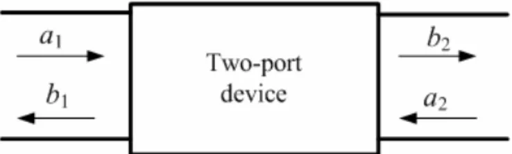
For a two-port network shown in Fig. 1, the chain-scattering parameters T (i, j ij
= 1, 2) are defined as follows:
⎥⎦
⎢ ⎤
⎣
⎥⎡
⎦
⎢ ⎤
⎣
=⎡
⎥⎦
⎢ ⎤
⎣
⎡
2 2
22 21
12 11
1 1
a b T T
T T b
a
(1)
where the waves a1 and b1 at port 1 are dependent variables, and the waves a2 and b2
at port 2 are independent variables. Table I [6] shows the chain-scattering parameter matrices of basic transmission lines, namely, series line, shunt-open stub, shunt-short stub, and shunt-open two-section stub.
The delay element in the discrete-time domain is obtained by setting
1 2j li i
z− =e− β (i = 1, 2, a, b, c), whereβ denotes the propagation constant, and li i is the transmission line length. Z0 is the characteristic impedance of the reference line. The chain-scattering parameters of a cascade connection of transmission lines can be determined by sequential multiplications of eachcomponent as expressed in (2).
⎥⎦
⎢ ⎤
⎣
= ⎡
⎥⎦
⎢ ⎤
⎣
⎡
∏
= i i
i N i
cascade i T T
T T T
T T T
22 21
12 11 22 1
21 12 11
(2) where N is the number of components, T11i,T12i ,T21i , and T22i are the matrix elements representing the i-th component.
Fig. 1 Two-port network with incident and reflected waves
Table 1 Chain-scattering parameter matrices of basic transmission lines
2.2 Stability Consideration
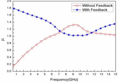
A broadband transistor generally fails to satisfy the unconditional stability requirement over the frequency band of interest. The stability factor μ [7] is less than 1 from DC to 6 GHz. To improve the stability, a series R-C negative feedback circuit connecting the gate and the drain is added to the transistor [8] with R = 350 Ω and C = 33 pF. Fig. 2 shows that this active component with a feedback circuit satisfies the unconditional stability condition for frequencies ranging from 0.5 GHz to 15 GHz.
Fig. 2 Stability factor μ with and without R-C feedback circuit
2.3 z-domain model of GaAs FET
MESFET scattering parameters have been studied by rational functions of angular frequency in the continuous domain [4]. Here, we examine the conversion of frequency-domain scattering parameters Sij (i, j = 1, 2) of the GaAs FET into discrete-time representations. We develop our software in the MATLAB environment [9]. For the conversion, the frequency range of interest is normalized so that the new scale is between 0 and π. The scattering parameter S(z) is set as follows:
1 1
( ) (0) (1) ... ( ) ( ) ( ) (0) (1) ... ( )
M N
B z b b z b M z
S z A z a a z a N z
− −
− −
+ + +
= =
+ + + (3)
where z−1 =e−jω and ω is the normalized frequency with 0≦ω≦π. Sequences b (m) (m = 0, 1, 2, …, M) and a(n) (n = 0, 1, 2,…, N) are real coefficients. The linear least squares (LLS) approximation [10] is adopted to determine sequences b (m) and
a(n), which is given by
2
, 1
min K ( )i ( ) ( )i i
a b i
B ω S ω Aω
=
∑
−(4)
where
0
( ) ( ) i
M j n
i n
B ω b m e− ω
=
=
∑
,1
( ) 1 ( ) i
N j n
i
n
Aω a n e−ω
=
= +
∑
and S( )ω is the original i GaAs FET scattering parameter at the normalized frequency ωi. To improve the effectiveness of the LLS algorithm, the following weighted factor associated with each frequency point of interest is employed:2
, 1 ( ) ( ) ( )
min K i i i
i b t
a W
∑
B w −S w A w= (5) where Wt is the weight factor that allows the fit-error to be monitored against the frequency of interest. The weighted LLS equation in (5) is the algorithm for simulating the conversion of scattering parameters from the frequency domain to the z-domain. In order to reduce noise during the simulation process, it is recommended that the order of the polynomial function in (3) be less than ten. The established discrete-time model of scattering parameters of a microwave transistor is expressed as
∑
∑
=
−
=
−
=
70 7
0
) (
) ( )
(
n
n ij
m
m ij
ij
Z n a
Z m b z
S
Sij (i, j = 1, 2) (6)We convert the frequency-domain scattering parameters of FSX017LG with the R-C feedback circuit into the z-domain representations. The obtained coefficients of discrete-time scattering parameter S11 are as follows:
11 =
b [-0.2066, -0.2274, 0.1694, 0.6392, 2.6048, 2.4266, 0.7030, 0.3583],
11 =
a [1.0000, 2.0844, 5.2831, 5.0297, 1.4926, 0.9067, -0.0234, -0.13750]. The coefficients of S12 are given as b12 =[0.0865, 0.0909, 0.2312, 0.3700, 0.1426, 0.0819, 0.0550, -0.0092], a12 =[1.0000, 0.7565, 2.1445, 2.9160, 0.0849, -0.0353, 0.1382, -0.0663].
The coefficients of S21 are expressed as b21 =[0.1094, -0.6858, -4.6244, -6.5157, -3.7606, -2.7228, -2.1664, -0.5829], a21 =[1.0000, 2.4040, 1.7242, 1.0089, 0.9269, 0.3135, 0.0170, -0.0064]. The corresponding coefficients of S22 are given as
22 =
b [-0.5595, -0.6549, 0.8147, 4.7817, 6.9509, 1.3299, -2.4432, -0.7535],
22 =
a [1.0000, 3.5009, 13.1768, 20.0389, 8.7844, -1.9793, -2.4918, -0.9717].
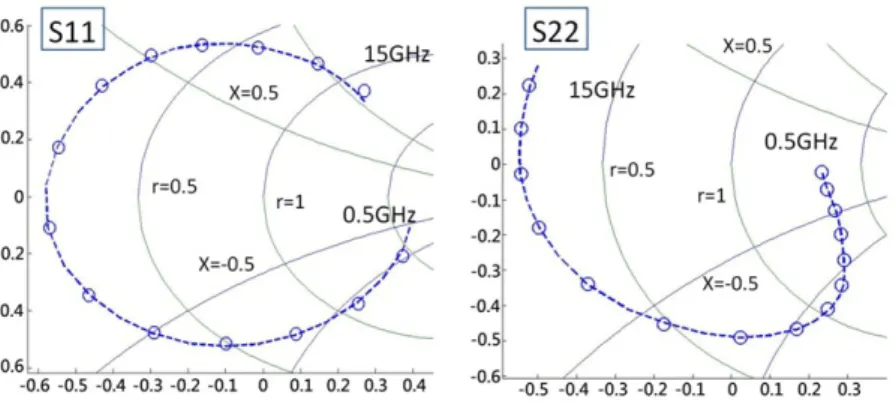
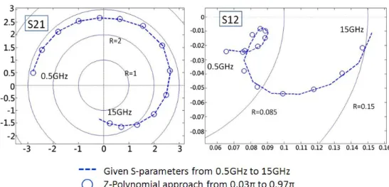
Fig. 3 shows S11 and S22 complex curves of both the z-domain model and the original data on Smith charts. Fig. 4 shows S12 and S21 complex curves. The complex responses of the z-domain model are in good agreement with their original data, except for the normalized frequencies ω = 0 and ω= π. When ω is π or 0, Sij(z) in (6) is real, which deviates from the original Sij(ω). However, such a limitation has little effect on practical implementation.
Fig. 3 S11 and S22 complex responses of original data and discrete z-domain model
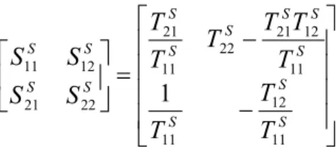
Fig. 4 S12 and S21 complex responses of original data and discrete z-domain model The scattering parameters can be converted to chain-scattering parameters by the following equation:
⎥⎥
⎥⎥
⎦
⎤
⎢⎢
⎢⎢
⎣
⎡
−
−
⎥=
⎦
⎢ ⎤
⎣
⎡
f f f f
f f
f f f
f f
f f
S S S S
S S
S S S
T T
T T
21 22 11 12 21 11
21 22
21 22
21 12 11
1
(7) As a result, the chain-scattering elements of the GaAs FET with the R-C feedback circuit are represented by equations 8 to 11, where
7 11 1
11 11
7 11 1
11 11
11 (1) (2) ... (8)
) 8 ( ...
) 2 ( ) 1 (
−
−
−
−
+ + +
+ +
= +
z a z
a a
z b z
b
T bft ft ft
ft ft
f ft
(8)
14 12
1 12 12
14 12
1 12 12
12 (1) (2) ... (15)
) 15 ( ...
) 2 ( ) 1 (
−
−
−
−
+ + +
+ +
= +
z a z
a a
z b z
b
T bft ft ft
ft ft
ft f
(9)
14 21
1 21 21
14 21
1 21 21
21 (1) (2) ... (15)
) 15 ( ...
) 2 ( ) 1 (
−
−
−
−
+ + +
+ +
= +
z a
z a a
z b z
b
T bft ft ft
ft ft
f ft
(10)
28 22
1 22 22
28 22
1 22 22
22 (1) (2) ... (29)
) 29 ( ...
) 2 ( ) 1 (
−
−
−
−
+ + +
+ +
= +
z a
z a a
z b
z b
T bft ft ft
ft ft
ft f
(11)
It is pertinent to point out that adapting z-polynomial to model a FET will cause
simulations because all mathematic calculations were processed within normalized frequency π. In this method, simulations outside normalized frequency will be ignored.
3. Design method and simulation results of broadband amplifier in z-domain
The input network can be represented by chain-scattering parameter matrices as follows:
⎥ ⎦
⎢ ⎤
⎣
= ⎡
⎥ ⎦
⎢ ⎤
⎣
⎡ ∏
= k k
k m k
In k In
In In
T T
T T T
T T T
22 21
12 11 22 1
21 12 11
(12)
where m denotes the number of transmission lines and Tijk
(i,j = 1,2) denotes the matrix element of the k-th component of the input network. The output network is given as
∏
=⎥
⎦
⎢ ⎤
⎣
= ⎡
⎥ ⎦
⎢ ⎤
⎣
⎡
nl l l
l l Out
Out
Out Out
T T
T T T
T
T T
1 21 22
12 11 22
21
12 11
(13)
where n denotes the number of transmission lines and T (i,j = 1,2) denotes the ijl matrix element of the l-th component of the output network.
The chain-scattering matrix of the overall amplifier system can be obtained by sequential multiplications of the chain-scattering matrices of the input network, microwave transistor, and output network, which is given as
11 12 11 12 11 12 11 12
21 22 21 22 21 22 21 22
. .
S S IN IN f f Out Out
S S IN IN f f Out Out
T T T T T T T T
T T T T T T T T
⎡ ⎤ ⎡ ⎤ ⎡ ⎤ ⎡ ⎤
⎢ ⎥ ⎢= ⎥ ⎢ ⎥ ⎢ ⎥
⎣ ⎦ ⎣ ⎦ ⎣ ⎦ ⎣ ⎦ (14)
The scattering parameters of the overall amplifier system can be obtained by the following conversion:
⎥⎥
⎥⎥
⎦
⎤
⎢⎢
⎢⎢
⎣
⎡
−
−
⎥=
⎦
⎢ ⎤
⎣
⎡
S S S
S S S S S S
S S
S S
T T T
T T T T
T T S
S S S
11 12
11
11 12 21 22 11 21
22 21
12 11
1
(15)
The parameter Ss21 is considered as the system function of the amplifier. To design an amplifier embedded with a band-pass filter, Ss21 is manifested to fit the
“magnified” band-pass filter prototype in the sense of the least squares error. We set the target amplitude response S21idea[ ]i of the “magnified” band-pass filter as a fifth-order Chebyshev band-pass filter with a constant power gain in the pass-band, as shown in Fig. 5. The range of |S21|2 of GaAs FET transistor FSX017LG in data sheet is 8<|S21|2 <10. In order to set an achievable gain over the wide pass-band, we select the gain of the amplifier as 9dB for the frequencies from 3.1GHz to 10.6GHz.The least squares error method is employed to minimize the deviation of Ss21 from S21idea[ ]i as follows:
∑
= K −i
idea
s i S i
S
1
2 21
21[] [ ]
min
(16)
Fig. 5 Target gain response
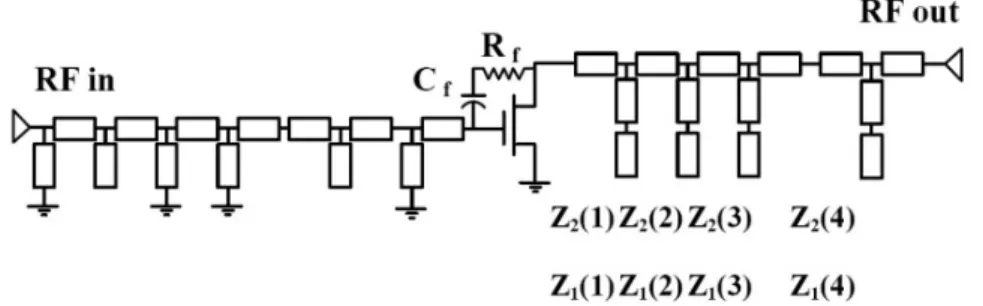
We select four short stubs, two open stubs, four two-section open-circuited stubs, as well as series unit lines as the basic matching networks. The configuration of the amplifier design is shown in Fig. 6. Notice that the circuit configuration in Fig.6 is selected to meet the required circuit response S21ideal shown in Fig.5. To simplified the optimization algorithm requirements for both S11 and S21 are neglected for the present consideration. A close look of Fig.6 indicates that there are six nulls in the frequency range of interest. Four equal-length two-section open stubs are employed to implement four zeros located at 0.125π,0.19π,0.71π and 0.79π. Four one-section stubs are used to the null at 0π, while two one-section open stubs are used to realized the null at π. Both of Rf and Cf are used to improve the stability of the microwave transistor so that the transistor maintains the unconditionally stable condition over the entire frequency range. As stated in section 2.2. We have Rf=350Ω and Cf=33pF.
Fig. 6 Configuration of ultra-wideband (UWB) amplifier embedded with band-pass filter
Upon substituting (8)–(11) and (17) into (14), The scattering parameters could be displayed as below:
Out f N Out f IN Out f IN Out f IN
S T T T T T T T T T T T T
T11 = 11 11 11 + 11 12 21 + 12 21 11 + 12 22 21
Out f N Out f IN Out f IN Out f IN
S T T T T T T T T T T T T
T12 = 11 11 12 + 11 12 22 + 12 21 12 + 12 22 22
Out f N Out f IN Out f IN Out f IN
S T T T T T T T T T T T T
T21 = 21 11 11 + 21 12 21 + 22 21 11 + 22 22 21
Out f N Out f IN Out f IN Out f IN
S T T T T T T T T T T T T
T22 = 21 11 12 + 21 12 22 + 22 21 12 + 22 22 22
The general scattering parameters of configuration of Fig.6 can be obtained in the parallel form as follows:
∑
∑
=
−
=
−
= 264
1
1 277
1
1
) (
) ( )
(
n
n ij m
m ij
S ij
Z n a
Z m b z
T +
∑
∑
=
−
=
− 271
1
1 284
1
1
) (
) (
n
n ij m
m ij
Z n a
Z m
b +
∑
∑
=
−
=
− 271
1
1 284
1
1
) (
) (
n
n ij m
m ij
Z n a
Z m
b +
∑
∑
=
−
=
− 292
1
1 305
1
1
) (
) (
n
n ij m
m ij
Z n a
Z m
b (18)
The direct form in (19) could be obtained by making reduction of fractions to a
common denominator of (18). The upper limits of sigmas are obtained by matlab numerical simulation in which the cascade connection of each micro-strip elements and the z-polynomial representation of FET. It is noteworthy that aij(n) and bij(m) in (18) and (19) are functions of characteristic impedances of the input and output transmission lines. As the result, the characteristic impedances of the transmission lines are obtained in the optimization process.
∑
∑
=
−
=
−
= 1095
1
1 1108
1
1
) (
) ( )
(
n
n ij
m
m ij
S ij
Z n a
Z m b z
T
(19) The high orders in both the numerator and the denominator of the polynomial in (19) can cause numerical noise [11]. Fig. 7 shows the simulation scattering parameters of the amplifier, which are obtained from the direct-form expression in (19). The numerical noise is generated by quantization process in the modeling. The quantization noise can arise in the digital implementation of the arithmetic operations involving the binary data due to the finite word length limitations of the registers storing the numbers and the results of the arithmetic operations.
Now consider how the roots of the denominator and numerator polynomials are affected by the errors in the coefficients. Clearly, each polynomial root is affected by all of the errors in the coefficients of the polynomial. Thus, each pole and zero will be affected by all of the quantization errors in the denominator and numerator polynomials, respectively. More specifically, Kaiser(1966) showed that if the Poles and zeros of high-order z-polynomials are located tightly, small errors in the coefficients of the denominator or nominator can cause large changes in poles and zeros in this direct-form expression. Therefore, poles and zeros of the direct-form structure are quite sensitive to the variation of the coefficients of high-order z-polynomials. Fig. 8 shows that the parallel-form function in (18) is generally much less sensitive to coefficient variation than the equivalent direct-form function. To reduce the numerical noise during the system simulation, the parallel-form polynomials of chain-scattering parameters were adopted in this study.
Fig. 8 Simulation results of S parameter frequency for parallel-form z-polynomials For the input matching circuit, the obtained characteristic impedances of open stubs, from left to right, are [145, 145 Ω]. The characteristic impedances of short stubs, from left to right are [145, 145, 145, 55.8 Ω]. The characteristic impedances of series unit lines, from left to right, are [31, 56, 29, 34, 48, 50, 27.3 Ω]. For the output
matching circuit, the characteristic impedances of two-section open-circuited stubs, from the left to the right, are (Z2(1),Z1(1)) = (90, 623 Ω), (Z2(2),Z1(2)) = (145, 591 Ω), (Z2(3),Z1(3)) = (145, 14 Ω), and (Z2(4),Z1(4)) = (145, 6 Ω). The characteristic impedances of series lines at the output, from the left to the right, are [68, 43, 35, 25, 31, 37.3 Ω].
The unattainable characteristic impedances of transmission-line sections are modified by the frequency-bandwidth-impedance relation of a notch filter. The relations between characteristic impedance, bandwidth Δ, and center frequency ΩN of a notch filter implemented with a two-section open stub are [12]
1 0
2
2 tan ( ) 2
Z Z
= −
Δ
(20) and
1 1 2
1 2
1 /
cos ( ),
1 /
N
Z Z Z Z
− −
= +
Ω
(21)
where Z0 is the reference characteristic impedance, which is 50 Ω. When the normalizing frequency is doubled and both Δ and ΩN are reduced to one half, the new attainable characteristic impedances are (Z′2(1),Z′1(1)) = (130, 67 Ω) and (Z′2(2),Z′1(2)) = (138, 55 Ω); when the normalizing frequency is reduced to one half and both Δ and ΩN are doubled, the new characteristic impedances are (Z′2(3),Z′1(3))
= (74.4, 37 Ω) and (Z′2(4),Z′1(4)) = (86, 20 Ω).
Notice that the characteristic impedance of the serial reference characteristic impedance is Zo for all basic elements, as shown in table1. The shunt elements are placed at the junctions between two finites lines. As a result, the formulas in both (20) and (21) relating the characteristic impedance, bandwidth Δ and center frequency of a notch filter are applicable. It is pertinent to point out the simulation results of using converted characteristic-impedances transmission lines are the same as those of using unattainable characteristic-impedance transmission lines for the circuit shown in Fig.6.
In other word, the outer impedances seen from the stubs are Zo.
4. Experimental Results
Figs. 9 and 10 show photographs of the proposed amplifier and the setup for measurement, respectively. The circuit is built on the UL2000 substrate with a thickness of 0.762 mm, relative dielectric constant of 2.45, and loss tangent of 0.0025.
Each finite line has an electrical length of λ/4 at a normalizing frequency of 15 GHz.
The physical lengths of two two-section open stubs Z′2(1), Z′1(1), Z′2(2), and Z′1(2) are λ/8 at the normalizing frequency of 15GHz; those of two two-section stubs Z′2(3), Z′1(3), Z′2(4), and Z′1(4) are λ/2 at the normalizing frequency of 15GHz.
Fig. 9 Photograph of proposed amplifier
Fig. 10 Photograph of experiment setup.
Two bias tees are used to supply DC voltage to the circuit. The bias voltage is 4 V, and the bias current is 30 mA. Four chip capacitors are employed as DC blocks
RF in
Bias Tee
VDS = 4 V
VGS = -0.5 V
RF out
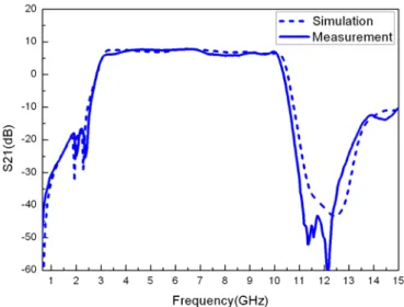
between the short stubs and ground at the input matching circuit. Four chip capacitors are employed as DC blocks between the short stubs and ground at the input matching circuit. Figs. 11–14 show the experimental results and RF simulation of S21, S12, S11, and S22, respectively. The measured S21 has a flat gain response for frequencies from 3.1 GHz to 10.6 GHz. In particular, S21 has a good fall-off rate in the stopband.
Fig. 11 S21 responses of proposed amplifier in microwave simulation and experimental result
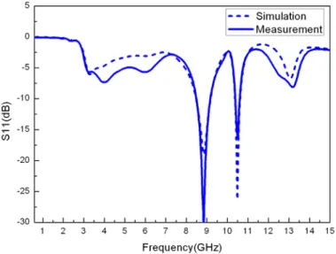
Fig. 13 S11 responses of proposed amplifier in microwave simulation and experimental result
Fig. 14 S22 responses of proposed amplifier in microwave simulation and experimental result
The system group delay and stability factor (μ) are shown in Fig. 15 and Fig. 16, respectively. The proposed amplifier is unconditionally stable over the entire frequency band of interest and has flat group delay. This amplifier could be used as a UWB amplifier in a transmitter.
Fig. 15 Group delay of proposed amplifier
Fig. 16 Stability factor μ of proposed amplifier
The Pin-Pout relation and intermodulation distortion IMD3 are shown in Fig.17.
Its power conversion efficiency is shown in Fig.18. The third-order power interception point IP3 of this amplifier is about 24dBm at 4GHz, 5GHz and 6GHz.
Fig. 17 Output Power and IMD3 of proposed amplifier
Fig. 18 Output power and efficiency of proposed amplifier 5. Conclusion
A discrete-time domain method was proposed to design an ultra-wideband amplifier embedded with a band-pass filter. The proposed amplifier achieves a flat gain response. Four pairs of complex conjugate roots of the fifth-order ultra-wideband Chebyshev band-pass filter in the z-domain are implemented with four two-section open stubs that give transmission zeros in the lower and upper stopbands. Therefore, it has good fall-off selectivity. In addition, the unattainable characteristic impedances of transmission-line sections at the output matching network are modified by the frequency-bandwidth-impedance method. The novel method provides a basis for the integration of microwave applications and discrete-time signal processes.
References
[1] H. Harada and R. Prasad, Simulation and Software Radio for Mobile Communications, Artech House, Norwood, MA, 2002.
[2] D.-C. Chang and C.-W. Hsue, “Design and implementation of filters using transfer functions in the Z domain,” IEEE Trans. Microwave Theory Tech., vol.49, no.5, pp.979-985, May 2001.
[3] D.-C. Chang and C.-W. Hsue, “Wide-band equal-ripple filters in nonuniform transmission lines,” IEEE Trans. Microwave Theory Tech., vol.50, no.4, pp.1114-1119, April 2002.
[4] K. Nagatomo, Y. Daido, M. Shimizu, and N. Okubo, “GaAs MESFET characterization using least squares approximation by rational functions,” IEEE Trans.
Microwave Theory Tech., vol. 41, no.2, pp.199-205, February 1993.
[5] Fujitsu Microelectronics, Ltd. The data sheet of FSX017LG, Edition 1.2, July 1999.
[6] L.-C. Tsai and C.-W. Hsue, “Dual-band bandpass filters using equal-length, coupled-serial-shunted lines and Z-transform technique,” IEEE Trans. Microwave Theory Tech., vol.52, no.4, pp.1111-1117, April 2004.
[7] M. L. Edwards and J. H. Sinsky, “A new criterion for linear 2-Port stability using a single geometrically derived parameter,” IEEE Trans. Microwave Theory Tech., vol.40, no.12, pp.2303-2311, December 1992.
[8] Y. Chung, S. Cai, W. Lee, Y. Lin, C. P. Wen, K. L. Wang, and T. Itoh, “High power wideband AIGaN/GaN HEMT feedback amplifier module with drain and feedback loop inductances,” Electronics Letters, vol.37, no.19, pp.1199-1200, September 2001.
[9] D. Hanselman and B. Littlefield, Mastering MATLAB 5, Prentice Hall, Englewood Cliffs, NJ, 1998.
[10] E. C. Levi, “Complex-curve fitting,” IRE Trans. Automatic Control, vol.AC-4, pp.37-44, 1959.
[11] A. V. Oppenheim, R. W. Schafer, and J. R. Buck, Discrete-time Signal Processing.
Chapter Six, Second Edition, Prentice Hall, Englewood Cliffs, NJ, 1999.
[12] C.-W. Hsue, C.-W. Ling, and W.-T. Hung, “Discrete-time notch filter and its application to microwave filter,” Microwave and Optical Tech. Lett., Vl. 50, vol.6, pp.1596-1600, 2008.
國科會補助計畫衍生研發成果推廣資料表
日期:2011/12/02
國科會補助計畫
計畫名稱: 利用Z-轉換技術設計及製作嵌入微波濾波器之微波放大器 計畫主持人: 徐敬文
計畫編號: 97-2221-E-011-023-MY3 學門領域: 電磁
無研發成果推廣資料
97 年度專題研究計畫研究成果彙整表
計畫主持人:徐敬文 計畫編號:97-2221-E-011-023-MY3 計畫名稱:利用 Z-轉換技術設計及製作嵌入微波濾波器之微波放大器
量化
成果項目 實際已達成
數(被接受 或已發表)
預期總達成 數(含實際已
達成數)
本計畫實 際貢獻百
分比
單位
備 註 ( 質 化 說 明:如 數 個 計 畫 共 同 成 果、成 果 列 為 該 期 刊 之 封 面 故 事 ...
等)
期刊論文 0 0 100%
研究報告/技術報告 0 0 100%
研討會論文 2 0 100%
論文著作 篇
專書 0 0 100%
申請中件數 0 0 100%
專利 已獲得件數 0 0 100% 件
件數 0 0 100% 件
技術移轉
權利金 0 0 100% 千元
碩士生 3 0 100%
博士生 1 0 100%
博士後研究員 0 0 100%
國內
參與計畫人力
(本國籍)
專任助理 0 0 100%
人次
期刊論文 4 0 100%
發 表 研 究 成 果 於 IEEE Microwave and Wireless Components
Letters 論文三篇 及 IEICE Trans.
Electron. 一篇。
研究報告/技術報告 0 0 100%
研討會論文 0 0 100%
論文著作 篇
專書 0 0 100% 章/本
申請中件數 0 0 100%
專利 已獲得件數 0 0 100% 件
件數 0 0 100% 件
技術移轉
權利金 0 0 100% 千元
碩士生 0 0 100%
博士生 0 0 100%
博士後研究員 0 0 100%
國外
參與計畫人力
(外國籍)
專任助理 0 0 100%
人次
其他成果
(
無法以量化表達之成果如辦理學術活動、獲 得獎項、重要國際合 作、研究成果國際影響 力及其他協助產業技 術發展之具體效益事 項等,請以文字敘述填 列。)
主 持 人 因 發 展 微 波 discrete-time domain technique 膺 選 為 2010 IEEE Fellow.
成果項目 量化 名稱或內容性質簡述
測驗工具(含質性與量性) 0
課程/模組 0
電腦及網路系統或工具 0
教材 0
舉辦之活動/競賽 0
研討會/工作坊 0
電子報、網站 0
科 教 處 計 畫 加 填 項
目 計畫成果推廣之參與(閱聽)人數 0
國科會補助專題研究計畫成果報告自評表
請就研究內容與原計畫相符程度、達成預期目標情況、研究成果之學術或應用價 值(簡要敘述成果所代表之意義、價值、影響或進一步發展之可能性) 、是否適 合在學術期刊發表或申請專利、主要發現或其他有關價值等,作一綜合評估。
1. 請就研究內容與原計畫相符程度、達成預期目標情況作一綜合評估
■達成目標
□未達成目標(請說明,以 100 字為限)
□實驗失敗
□因故實驗中斷
□其他原因 說明:
2. 研究成果在學術期刊發表或申請專利等情形:
論文:■已發表 □未發表之文稿 □撰寫中 □無 專利:□已獲得 □申請中 ■無
技轉:□已技轉 □洽談中 ■無 其他:(以 100 字為限)
發表研究成果於 IEEE Microwave and Wireless Components Letters 論文三篇及 IEICE Trans. Electron. 一篇。
3. 請依學術成就、技術創新、社會影響等方面,評估研究成果之學術或應用價 值(簡要敘述成果所代表之意義、價值、影響或進一步發展之可能性)(以 500 字為限)
本計畫利用 z-domain 技術完成 UWB ( 3.1GHz-10.6GHz ) 寬帶微波放大器,為國內通訊 產業發展 UWB 通訊系統磸定基礎。利益用 z-domain 技術設計微波放大器,具創新性,亦 為一般微波放大器設計,提供電路基本架構,具學術與實務價值。未來將利用此技術發展 LTE 基地站用 40 watts 射頻功率放大器。
![Fig. 8 Simulation results of S parameter frequency for parallel-form z-polynomials For the input matching circuit, the obtained characteristic impedances of open stubs, from left to right, are [145, 145 Ω]](https://thumb-ap.123doks.com/thumbv2/9libinfo/9128618.412709/15.892.176.713.503.967/simulation-parameter-frequency-parallel-polynomials-matching-characteristic-impedances.webp)