Balanced carrier transport in organic solar cells employing embedded
indium-tin-oxide nanoelectrodes
Min-Hsiang Hsu, Peichen Yu, Jen-Hsien Huang, Chia-Hua Chang, Chien-Wei Wu, Yu-Chih Cheng, and Chih-Wei Chu
Citation: Applied Physics Letters 98, 073308 (2011); doi: 10.1063/1.3556565 View online: http://dx.doi.org/10.1063/1.3556565
View Table of Contents: http://scitation.aip.org/content/aip/journal/apl/98/7?ver=pdfcov Published by the AIP Publishing
Articles you may be interested in
Erratum: “Balanced carrier transport in organic solar cells employing embedded indium-tin-oxide nanoelectrodes” [Appl. Phys. Lett.98, 073308 (2011)]
Appl. Phys. Lett. 98, 119904 (2011); 10.1063/1.3568898
Large-area organic solar cells with metal subelectrode on indium tin oxide anode Appl. Phys. Lett. 96, 173301 (2010); 10.1063/1.3419925
Embedded indium-tin-oxide nanoelectrodes for efficiency and lifetime enhancement of polymer-based solar cells
Appl. Phys. Lett. 96, 153307 (2010); 10.1063/1.3395395
Use of fluorine-doped tin oxide instead of indium tin oxide in highly efficient air-fabricated inverted polymer solar cells
Appl. Phys. Lett. 96, 133506 (2010); 10.1063/1.3374406
Origin of the light intensity dependence of the short-circuit current of polymer/fullerene solar cells Appl. Phys. Lett. 87, 203502 (2005); 10.1063/1.2130396
This article is copyrighted as indicated in the article. Reuse of AIP content is subject to the terms at: http://scitation.aip.org/termsconditions. Downloaded to IP: 140.113.38.11 On: Wed, 30 Apr 2014 09:18:07
Balanced carrier transport in organic solar cells employing embedded
indium-tin-oxide nanoelectrodes
Min-Hsiang Hsu,1,a兲 Peichen Yu,1,b兲 Jen-Hsien Huang,2,3 Chia-Hua Chang,1 Chien-Wei Wu,4Yu-Chih Cheng,1and Chih-Wei Chu2
1
Department of Photonics and Institute of Electro-Optical Engineering, National Chiao-Tung University, Hsinchu 30010, Taiwan
2
Research Center for Applied Sciences, Academia Sinica, Taipei 11529, Taiwan
3
Department of Chemical Engineering, National Taiwan University, Taipei 10617, Taiwan
4
Department of Electrophysics, National Chiao-Tung University, Hsinchu 30010, Taiwan
共Received 1 November 2010; accepted 27 January 2011; published online 17 February 2011兲 In this paper, we present evidence of balanced electron and hole transport in polymer-fullerene based solar cells by means of embedded indium-tin-oxide nanoelectrodes. Enabled by a controllable electrochemical deposition, the individual nanoelectrodes are uniformly enclosed by a poly共3,4-ethylenedioxythiophene兲 hole-conducting layer, allowing a relatively short route for holes to reach the anode and hence increasing the effective hole mobility. Consequently, the power conversion efficiency and photogenerated current are maximized with a deposition condition of 50 C, where the ratio of the electron to hole mobility is nearly unity. © 2011 American Institute of Physics. 关doi:10.1063/1.3556565兴
Since solution-processed bulk-heterojunction 共BHJ兲 so-lar cells were reported for organic photovoltaics 共OPVs兲 in the mid-1990s,1such systems have been a popular subject of intense research. Owing to the random blends of donorlike conjugated polymers and acceptorlike fullerene molecules, strongly disordered interfaces inside the mix and hopping processes between chain segments of the conjugated polymer result in an insulatorlike behavior for organic photoactive materials.2 Consequently, ineffective carrier conduction be-comes one of the limiting factors of power conversion effi-ciency共PCE兲. Particularly, if charge transport inside the light absorbing materials is severely unbalanced, as discovered in the mixture of regioregular poly共3-hexylthiophene兲 共P3HT兲 and关6,6兴-phenyl-C60-butyric acid methyl ester 共PCBM兲, the low mobility of holes could cause charge accumulation near the anode, leading to a space charge limit current 共SCLC兲.3 In order to restrain the build-up space charges, major re-search efforts have been concentrated on adjusting the blend ratio, annealing conditions, and so on to achieve balanced carrier mobilities,4–6 which may limit the material selection in OPVs. Although recent advances in nanofabrication tech-nologies have permitted the formation of bicontinuous and interdigitated networks, no clear evidence has been demon-strated as to the improvement of carrier conduction.7In this work, we present an alternative to balance charge transport by means of buried electrodes made of indium-tin-oxide 共ITO兲 nanorods.8,9
The free-standing nanoelectrodes 共NEs兲 are protruded into organic active materials, offering three-dimensional 共3D兲 collection pathways for low mobility holes. Further enabled by a controllable electrochemical deposition 共ECD兲 of a hole conducting layer 共HCL兲 wrap-ping around individual NEs, we show evidence of balanced electron and hole transport in polymer-fullerene based solar cells.
The randomly-oriented nanorods were deposited on 260-nm-thick ITO-coated glass substrates using oblique electron-beam evaporation in an oxygen deficient environ-ment. The rod formation involved a two-step process known as nucleation and column growth via surface diffusion, as-sisted by the introduced nitrogen. We have found that the obliquely incident vapor reduces the flux density of mol-ecules on the surface, which facilitates the separation and formation of nuclei. Moreover, the oxygen deficiency allows the segregation of tin-doped indium to form a liquid surface that promotes the absorption of incident vapors, re-sulting in vertical column growth.10 To function properly as embedded NEs in OPV devices, a uniform coating of a HCL enclosing the nanostructures is essential in order to effec-tively block electrons. Our previous work employed the con-ventional spin-casting of poly-共3,4-thylenedioxythiophene兲: poly共styrenesulfonate兲 共PEDOT:PSS兲, which exhibited poor adhesion to the NEs and slightly increased the leakage current.10 On the other hand, the excellent conductivity of ITO NEs suggested the feasibility of a HCL via ECD.10The ECD process used to gradually polymerize the EDOT onto the ITO NEs is chemically scalable and controllable, and thus is relatively cost effective and also roll-to-roll compat-ible. Here, a triple-terminal electrochemical cell that com-prised a counter, reference, and working electrode was em-ployed with selected charge quantity settings at an applied voltage of 1.1 V. The ECD process resulted in PEDOT coat-ings of various thicknesses that uniformly wrapped around the 3D NEs. Figures 1共a兲–1共f兲 show the surface morpholo-gies of PEDOT deposited with a charge quantity setting of 0 C, 25 C, 50 C, 250 C, 500 C on the NEs, and on a conventional 260-nm-thick ITO film at 500 C, respec-tively. As shown in Fig.1共a兲, the bare free-standing NEs are about 30 nm thick and 150 nm long with an estimated den-sity of 2⫻1010 cm−2. The spacing between NEs is on the order of a few tens to over a hundred nanometers, which is sufficient for the penetration of active materials without al-tering the organization of BHJ morphology.11With a charge
a兲Author to whom correspondence should be addressed. Electronic mail:
b兲Electronic mail: [email protected].
APPLIED PHYSICS LETTERS 98, 073308共2011兲
0003-6951/2011/98共7兲/073308/3/$30.00 98, 073308-1 © 2011 American Institute of Physics
This article is copyrighted as indicated in the article. Reuse of AIP content is subject to the terms at: http://scitation.aip.org/termsconditions. Downloaded to IP: 140.113.38.11 On: Wed, 30 Apr 2014 09:18:07
setting of 25 C, the deposited PEDOT layer is barely de-tectable关Fig. 1共b兲兴. Increasing the charge setting to 50 C gives rise to slightly thicker NEs关Fig.1共c兲兴. The deposition
condition also leads to a strong electric field near the tips of NEs, resulting in a thicker PEDOT on the top than the bottom.12The vertical distribution of EDOT polymerization rates becomes rather discernible with large charge quantities. As seen in Figs.1共d兲and1共e兲, the growth of PEDOT on the tips of NEs exceeds that on the bottom and hence forms cross-linked networks at the deposition conditions of 250 C and 500 C, respectively. For comparison, the deposition of PEDOT on a conventional ITO film electrode at 500 C is shown in Fig. 1共f兲, which reveals a relatively dense porous structure. The coated PEDOT is ⬃25 nm thick.
Figures 2共a兲–2共f兲 show the atomic force microscopic 共AFM兲 analysis and an estimated surface roughness for structures seen in Figs. 1共a兲–1共f兲, respectively. The mor-phologies of NEs shown in Fig. 2 do not resemble those in Fig.1 which are mainly limited by the AFM tip dimension. Nevertheless, the surface analysis provides a qualitative as-sessment of morphology variations in ITO NEs at different deposition conditions. As seen in Figs.2共b兲–2共e兲, the surface
roughness first increases at the beginning of deposition and then decreases with the increased charge settings due to a gradual planarization of the excess PEDOT. However, the surface morphology with the ITO NEs is still much rougher than that with the film electrode at the same charge quantity of 500 C.
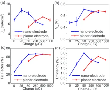
For practical devices, we prepared relatively short ITO NEs with heights around 100–150 nm in order to achieve adequate roughness while uniformly controlling the coating of a HCL. The 200-nm-thick active region was composed of a mixture of P3HT and PCBM with a weight ratio of 1:1 into 1,2-diochlorobenzene, which was spin-cast onto the PEDOT layer. The calcium and aluminum with respective thicknesses of 30 nm and 60 nm were subsequently capped by thermal evaporation at 10−5 torr. Moreover, a reference device with a conventional ITO planar electrode 共PE兲 was fabricated with the same process procedures at the same time. The current-voltage characteristics of polymer-fullerene blended solar cells are plotted as a function of the ECD charge setting in Figs.3共a兲–3共d兲, which correspond to the short-circuit current density 共Jsc兲, open-circuit voltage 共Voc兲, fill factor 共FF兲, and the PCE, respectively. The cells with PEDOT on a conven-tional PE were first optimized with various charge settings to determine the best condition at 500 C for reference. As seen in Fig.3共a兲, the photocurrent achieves over 9 mA/cm2 at 25 C, and gradually deteriorates, which could result from both the planarization共Fig.2兲 and parasitic absorption
of PEDOT. A quick estimation based on measured transmit-tance spectra reveals that the absorption in PEDOT at 500 C accounts for a decrease in Jsc by less than 0.3 mA/cm2. Therefore, the planarization of PEDOT is the dominant factor in the photocurrent reduction. By comparing the NE morphologies shown in Figs. 1共c兲 and 1共d兲, the 50 C charge setting represents a critical PEDOT layer thickness, where photocurrent is still high and the NEs re-main distinctive without forming a cross-linked PEDOT net-work. The fast growing PEDOT at large charge settings pla-narizes NEs with distributed porosities and voids which diminish the purpose of embedded electrodes and hinder the device performance 共Fig.3兲. Nevertheless, the large
photo-(a) (b)
(c) (d)
(e) (f)
FIG. 1. Scanning electron microscopic images of 共a兲 free-standing ITO
nanorods deposited on a 260-nm-thick ITO film; those in共a兲 coated with
PEDOT by ECD at共b兲 25 C,共c兲 50 C,共d兲 250 C, and共e兲 500 C.共f兲
The deposition of PEDOT on a controlled ITO film at 500 C. The scalar
bars are 200 nm.
(e) (a)
(f)
Mean Roughness: 11.12nm Mean Roughness: 16.71nm
Mean Roughness: 14.96nm
Mean Roughness: 10.78nm Mean Roughness: 5.32nm
50nm 30nm 10nm -10nm (d) (c) Mean Roughness: 12.49nm (b)
FIG. 2. 共Color online兲 关共a兲–共f兲兴 AFM analyses for the samples shown in
Figs.1共a兲–1共f兲, respectively.
(a) 0 25 50 250 500 1000 (b) 0 25 50 250 500 1000 (c) (d) 0 25 50 250 500 1000 0 25 50 250 500 1000 4 6 8 10 Jsc (mA/cm 2 ) Charge (C) nano-electrode planar electrode 0.3 0.4 0.5 0.6 Voc (V) Charge (C) nano-electrode planar electrode 0 20 40 60 80 Fill Fact or (%) Charge (C) nano-electrode planar electrode 0.0 0.5 1.0 1.5 2.0 2.5 3.0 3.5 Efficiency (% ) Charge (C) nano-electrode planar electrode
FIG. 3. 共Color online兲 The current-voltage characteristics of
polymer-fullerene solar cells with embedded NEs and a controlled PE coated with
PEDOT by an electrochemical method with various charge quantities:共a兲
short-circuit current, Jsc,共b兲 open-circuit voltage, Voc,共c兲 FF, and 共d兲 PCE.
073308-2 Hsu et al. Appl. Phys. Lett. 98, 073308共2011兲
This article is copyrighted as indicated in the article. Reuse of AIP content is subject to the terms at: http://scitation.aip.org/termsconditions. Downloaded to IP: 140.113.38.11 On: Wed, 30 Apr 2014 09:18:07
current in Fig.3共a兲suggests that the ECD can result in a thin layer of PEDOT onto ITO nanorods with low charge set-tings. However, as the work function of anode also varies with the HCL thickness at the beginning of deposition,13an extremely thin PEDOT layer may result in a Schottky barrier on the contact, which in turn increases the saturation current and the series resistance.14,15Therefore, the Vocand FF are relatively small at 25 C but peaked at 50 C, as seen in Figs. 3共b兲 and 3共c兲, respectively. Further increasing the charge setting does not affect Vocand FF significantly, owing to the formation of Ohmic contacts. As a result, the cell with ITO NEs achieves the highest PCE of 3.02% with a charge quantity of 50 C at which the condition is much lower than the best film device at 500 C. The discrepancy in the optimized deposition condition may arise from a thicker PEDOT deposition on the NEs than on the PE with the same charge setting 共see Ref. 16兲 for transmittance
characteriza-tion兲. Overall, the Jsc and PCE are, respectively, improved by 10.1% and 13.1%, compared to the film reference. It is also worth noting that the FF achieves 66.2%, which is su-perior to our previous device at 58.7% using a spin-casting method for the HCL.10The improvement is mostly attributed to the prominent particle-by-particle electropolymerization of EDOT onto the NEs, which prevent NEs from shunting the cathode while improving the contact resistance.
The 3D NEs protruded into the photoactive material pro-vide shorter routes for hole conduction than the PE. As a result, the time it took for holes to arrive at the anode is reduced, prompting an increase in effective hole mobility with respect to the film electrode. Under the assumption, the hole and electron mobilities can be obtained from the current-voltage characteristics of unipolar devices based on a SCLC model.17 First, the calcium top-contact was replaced by MoO3by thermal evaporation to make hole-only devices. Next, Cs2CO3 dissolved in 2-ethoxyethanol was spin-cast
onto the ITO NEs to replace PEDOT for electron-only de-vices. As seen in Fig. 4, the short-circuit current density is indeed highly correlated with the ratio of the electron to hole mobility. The highest two photocurrent occurring at either 25 or 50 C are both very close to the conditions where the mobility ratio is nearly unity. When deviating from the ideal charge settings, the electron and hole mobilities are unbal-anced again, leading to a potential SCLC dictated by the quarter power of the lower carrier mobility.3 However, as seen in Fig.3共c兲, the FF at 250 and 500 C are nearly the same, which eliminates the occurrence of a shunt current due to the SCLC. The photocurrent in these devices is most likely limited by the planarization and parasitic optical ab-sorption of PEDOT.
We thank Professor B. Q. Sun at the Functional Nano & Soft Materials Laboratory 共FUNSOM兲 at the Soochow Uni-versity for fruitful discussions. This work is founded by Na-tional Science Council in Taiwan under grant number NSC96-2221-E-009-092-MY3, NSC 98-2112-M-001-022-MY3.
1J. J. M. Halls, C. A. Walsh, N. C. Greenham, E. A. Marseglia, R. H.
Friend, S. C. Moratti, and A. B. Holmes, Nature共London兲 376, 498
共1995兲.
2R. J. Kline, M. D. McGehee, and M. F. Toney,Nature Mater. 5, 222
共2006兲.
3P. W. M. Blom, V. D. Mihailetchi, L. J. A. Koster, and D. E. Markov,Adv.
Mater. 19, 1551共2007兲.
4Y. Kim, S. Cook, S. M. Tuladhar, S. A. Choulis, J. Nelson, J. R. Durrant,
D. D. C. Bradley, M. Giles, I. McCulloch, C.-S. Ha, and M. Ree,Nature
Mater. 5, 197共2006兲.
5F. Padinger, R. S. Rittberger, and N. S. Sariciftci,Adv. Funct. Mater. 13,
85共2003兲.
6W. Ma, C. Yang, X. Gong, K. Lee, and A. J. Heeger,Adv. Funct. Mater.
15, 1617共2005兲.
7B. C. Thompson and J. M. J. Fréchet,Angew. Chem., Int. Ed. 47, 58
共2008兲.
8M. Niggemann, M. Glatthaar, A. Gombert, A. Hinsch, and V. Witter,Thin
Solid Films 451–452, 619共2004兲.
9J. H. Huang, Z. Y. Ho, D. Kekuda, C. W. Chu, and K. C. Ho, J. Phys.
Chem. C 112, 19125共2008兲.
10P. Yu, C. H. Chang, M. H. Su, M. H. Hsu, and K. H. Wei,Appl. Phys. Lett.
96, 153307共2010兲.
11S. S. V. Bavel, E. Sourty, G. D. With, and J. Loos,Nano Lett. 9, 507
共2009兲.
12G. Marshall, P. Mocskos, H. L. Swinney, and J. M. Huth,Phys. Rev. E 59,
2157共1999兲.
13Y. Shi, S. C. Luo, W. Fang, K. Zhang, E. Mohamed Ali, F. Y. C. Boey, J.
Y. Ying, J. Wang, H. H. Yu, and L. J. Li,Org. Electron. 9, 859共2008兲.
14Y. Kim, A. M. Ballantyne, J. Nelson, and D. D. C. Bradley,Org. Electron.
10, 205共2009兲.
15M. C. Arenas, N. Mendoza, H. Cortina, M. E. Nicho, and H. Hu, Sol.
Energy Mater. Sol. Cells 94, 29共2010兲.
16See supplementary material at http://dx.doi.org/10.1063/1.3556565 for
transmittance characterization.
17V. Shrotriya, Y. Yao, G. Li, and Y. Yang,Appl. Phys. Lett. 89, 063505
共2006兲. 0 25 50 250 500 6 7 8 9 Jsc μe/μh Charge (μC) J sc (mA/c m 2 ) 0 1 2 3 R at io of car rier mob ilit y
FIG. 4. 共Color online兲 The short-circuit current Jscand the ratio of electron
to hole mobility共e/h兲 are plotted as a function of the charge quantity in
the ECD of PEDOT.
073308-3 Hsu et al. Appl. Phys. Lett. 98, 073308共2011兲
This article is copyrighted as indicated in the article. Reuse of AIP content is subject to the terms at: http://scitation.aip.org/termsconditions. Downloaded to IP: 140.113.38.11 On: Wed, 30 Apr 2014 09:18:07