國立臺灣大學電機資訊學院電子工程學研究所 碩士論文
Graduate Institute of Electronics Engineering College of Electrical Engineering & Computer Science
National Taiwan University master thesis
一個在切換頻率中利用電流平均控制來減低暫態漣波 的控制方法之直流降壓式轉換器
A Current Average Control Method for Transient-Ripple Reduction in Frequency Hopping DC-DC Converters
戴嘉南 Tai Jia-Nan
指導教授:陳信樹 博士 Advisor : Chen Hsin-Shu, Ph.D.
中華民國 100 年 1 月
January, 2011
致謝
這本論文能順利完成,首先要感謝的是指導教授陳信樹博士這些日子來的指 導和照顧,老師豐富的經驗替我解決了不少研究上所遇到的問題,也教導我正確 的研究態度及獨立研究的能力,讓我的研究可以順利完成。此外,感謝陳怡然教 授及陳昭宏教授在我碩士生涯中不曾間斷的給予指導,使得我在研究之路上不致 偏離,同時也感謝以上三位教授撥冗擔任我的口試委員,他們寶貴的意見使我獲 益良多。
感謝實驗室的學長、同學、學弟們,宏維、菁華、裕翔、泓霖、偉賢、偉志、
威廷、碩宏、依峻、宏彥、邦寧、傑帆及學弟們。另外感謝逸霈、邦榮、濠瞬、
立偉、凱宇、立言、后鍾,感謝你們在研究上的幫助。
感謝大學同學博煌、國瑋、運鋼、育嘉,雖然在就讀研究所後研究領域不盡 相同,但是感謝你們在百忙之中抽空排解我的鬱悶。
碩士生涯路途漫漫,求學之外我想特別感謝一個人:郁文,在紙醉金迷的台 北,孤單地困在我編織的封閉世界中,和一隻貓咪Hiro癡癡地等著我。我希望能 像這本論文一樣,痛苦會過去,美會留下。
最後,感謝我的父母,不肖的我延長了您們的工作年限,希望我的畢業能為 家帶來些微的幫助,能讓我報答養育之恩。
摘要
本論文闡述一個切換頻率中利用電流平均控制來減低暫態漣波控制方法的直 流電壓轉換器,並以台積電0.35-μm 2P4M 3.3V/5V Mixed Signal CMOS製程製作。
當使用切換頻率技術時,由於電感的電流連續性,使得切換頻率前和切換頻率後 所產生的電感電流交流值不同,在輸出電容產生出一暫態漣波電壓,此論文提出 一個如何控制電感電流才能使之無此暫態漣波電壓,其方式為利用延長或縮短充 電(放電)電流的時間來達到平均電感電流,此時間為切換頻率前後充電(放電)電 感電流時間的平均值,實現方式是利用額外電路準確計算此時間後,以脈衝的型 式插入原本的脈衝調變訊號。
依據量測的結果,本晶片的切換頻率設定在880k-3.4MHz,暫態漣波在頻域上 改進14.1dB,時域上改進88%。跳頻技巧最多可使EMI降低23.55dB,功率效率最
高為90%。晶片總面積占2.126mm2,而其它的量測結果也包含在本論文內。
Abstract
This thesis presents an inductor current average control method for transient-ripple reduction in frequency hopping DC-DC converters and is implemented in a standard 0.35-μm 2P4M 3.3V/5V Mixed Signal CMOS process. When using the frequency-hopping technique, there is transient ripple on the output voltage due to the difference of inductor current between two different frequencies. This thesis proposes a method which predicts the average inductor current and inserts a calculated-width pulse between two frequencies to reduce the transient ripple on the output voltage.
Measurement results are performed with the switching frequency of this chip operating between 0.88 MHz and 3.4 MHz. The transient ripple on the output voltage is reduced by 88% and the undesired spur is reduced by 14.1 dB. The frequency-hopping technique achieves 23.55 dB reduction of the EMI spur magnitude. The maximum power efficiency achieved 90%. The chip occupied 2.126 mm2, and the other detailed measurements are included in this thesis.
Table of Contents
致謝 ... I 摘要 ... II Abstract ... III Table of Contents ... IV List of Figures ... VI List of Tables ... X
Chapter 1 Introduction ... 1
1.1 Motivation ... 1
1.2 Thesis Organization ... 2
Chapter 2 Fundamental of DC-DC Buck Converter ... 3
2.1 Performance Metrics... 3
2.1.1 Efficiency ... 3
2.1.2 Regulation ... 4
2.1.2.1 Line Regulation ... 4
2.1.2.2 Load Regulation ... 5
2.1.2.3 Temperature Regulation ... 5
2.1.3 Transient Response ... 6
2.2 Architecture of DC-DC Converters ... 8
2.2.1 DC-DC Buck Converter Operation ... 8
2.2.2 Estimation of Output Voltage Ripple ... 13
2.2.3 Feedback-Loop Stabilization ... 15
2.3 Variable Frequency ... 18
2.3.1 Random Switching ... 19
2.3.2 Frequency Hopping ... 21
Chapter 3 Proposed Architecture ... 23
3.1 Introduction ... 23
3.2 Specification of DC-DC Buck Converter ... 23
3.3 System Architecture ... 24
3.4 Inductor Current Average Control (ICAC) ... 25
3.4.1 Hopping in Off Duty Cycle Period ... 28
3.4.1.1 Hopping frequency from low to high ... 28
3.4.1.2 Hopping frequency from high to low ... 31
3.4.2 Hopping in On Duty Cycle Period ... 32
3.4.2.1 Hopping frequency from low to high & from high to low ... 32
Chapter 4 Circuit Implementation and Simulation Results ... 34
4.1 Amplifier Circuit ... 35
4.1.1 Error Amplifier ... 35
4.1.2 Operational Amplifier ... 37
4.3 Ramp Generator Circuit ... 41
4.4 Digital-to-Analog Converter (DAC) ... 45
4.5 Inductor Current Average Control (ICAC) ... 47
4.5.1 Sample and Hold Circuit (S&H) ... 49
4.5.2 Calculated Pulse Circuit ... 51
4.5.3 Consideration of Delay Time ... 55
4.6 Gate Driver with Dead Time Control ... 58
4.7 Power Stage Circuit ... 60
4.8 Simulation Results ... 63
4.8.1 Frequency Hopping ... 64
4.8.1.1 Spectrum ... 65
4.8.1.2 Transient Ripple on the Output Voltage ... 66
4.8.2 Efficiency ... 69
4.9 Performance Summary in simulation ... 70
Chapter 5 Experiment Results ... 71
5.1 Measurement Setup ... 71
5.2 Measurement Results ... 78
5.2.1 Static Measurement before using the Frequency-Hopping Technique .. 78
5.2.2 Frequency Hopping ... 79
5.2.2.1 Spectrum ... 79
5.2.2.2 Transient Ripple on the Output Voltage ... 82
5.2.3 EMI Reduction ... 88
5.2.4 Efficiency ... 90
5.3 Performance Summary ... 92
Chapter 6 Conclusion and Future Work ... 93
6.1 Conclusion ... 93
6.2 Future Work ... 93
Bibliography ... 94
List of Figures
Chapter 2
Fig. 2.1 The definition of efficiency in the switching regulator………4
Fig. 2.2 Circuit diagram of the switching converter………..7
Fig. 2.3 The transient response of output voltage when a dynamic load is applied……..8
Fig. 2.4 Buck converter (a) the switch in 1 (b) the switch in 2……….9
Fig. 2.5 Steady-state output waveform Vs(t)………..9
Fig. 2.6 Output characteristic of buck converters………10
Fig. 2.7 (a) The diagram and waveforms of continuous mode (b) The waveforms of discontinuous mode……….12
Fig. 2.8 Buck converter (a) circuit (b) steady-state inductor current waveform……….13
Fig. 2.9 Output capacitor voltage and current waveforms for the buck converter in Fig.2.6……….14
Fig. 2.10 The simply operation of the PWM converter………...16
Fig. 2.11 The transfer function of feedback system………16
Fig. 2.12 Type II compensator with two poles and a zero………...17
Fig. 2.13 Type III compensator with three poles and two zeroes………18
Fig. 2.14 Switching parameters………...19
Fig. 2.15 Switching signal with randomized modulation (a)RPPM (b)RPWM (c)RCFMFD (d)RCFMVD (e)FH………...20
Fig. 2.16 Output spectrum of different switching schemes……….22
Fig. 2.17 Transient waveform of different switching schemes………22
Chapter 3 Fig. 3.1 Structure of a conventional PWM buck converter……….25
Fig. 3.2 Energy spread to multiple frequencies with the FH technique………..26
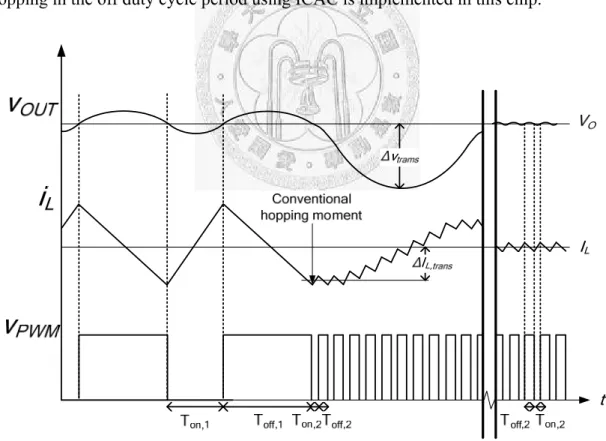
Fig. 3.3 Transient waveforms of output voltage, inductor current and PWM signal in a conventional converter………27
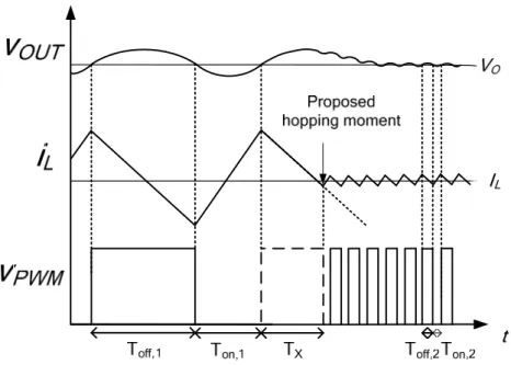
Fig. 3.4 Transient waveforms of output voltage, inductor current and PWM signal in the converter with the proposed ICAC technique………..28
Fig. 3.5 (a) Conventional and (b) proposed transient inductor current that hops frequency from low to high in off duty cycle………..29
frequency from high to low in off duty cycle period………...32
Fig. 3.7 Proposed transient inductor current that hops frequency from low to high in on duty cycle period……….33
Fig. 3.8 Proposed transient inductor current that hops frequency from high to low in on duty cycle period……….33
Chapter 4 Fig. 4.1 Block diagram of the FH buck converter with ICAC controller………34
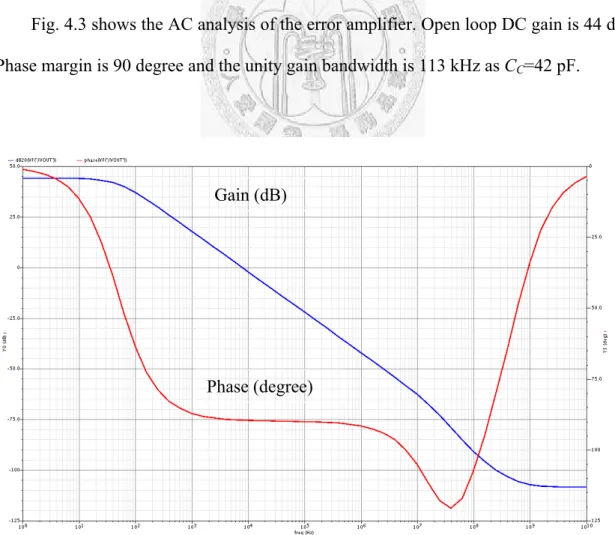
Fig. 4.2 Schematic of the error amplifier……….36
Fig. 4.3 Frequency response of the error amplifier……….36
Fig. 4.4 Schematic of folded-cascade operational amplifier………...38
Fig. 4.5 Frequency response of the OP-Amp without output buffer………...39
Fig. 4.6 Frequency response of the OP-Amp with output buffer………....39
Fig. 4.7 Common- drain output buffer (a) circuit. (b) small-signal equivalent circuit.. 40
Fig. 4.8 Schematic of the comparator……… 41
Fig. 4.9 Schematic of ramp generator……… 43
Fig. 4.10 The circuit of SR latch……… 43
Fig. 4.11 The simulation result of ramp generator………. 44
Fig. 4.12 The simulation of frequency considering process variation………... 45
Fig. 4.13 Schematic of DAC……….. 46
Fig. 4.14 INL and DNL of DAC……… 46
Fig. 4.15 Ramp generator without S&H in front end………. 48
Fig. 4.16 Ramp generator with S&H in front end and calculated pulse circuit in parallel……….48
Fig. 4.17 Circuit of the sample and hold……….49
Fig. 4.18 Diagram of the detector of hopping……….49
Fig. 4.19 Diagram of the control signal of sample time………..50
Fig. 4.20 Relationship between voltage and time length in a ramp signal………..51
Fig. 4.21 (a) Diagram of the additional ramp generators (b) Output of additional ramp generators……… 52
Fig. 4.22 Diagram of full Ramp generators……… 53
Fig. 4.23 Diagram of the calculated-width pulse circuit……… 53
Fig. 4.24 Transient waveform of ICAC……….. 54
Fig. 4.25 Waveform of calculated pulse including delay of components……….. 55
Fig. 4.26 Transient waveform of offset of the comparator………. 57
Fig. 4.27 Schematic of the gate driver with dead time control………59
Fig. 4.28 The simulation result of the gate driver with dead time control………..60
Fig. 4.29 Schematic of the power stage………...61
Fig. 4.30 Simulation of on-resistance of PMOS………..62
Fig. 4.31 Floor plan of the power stage on chip………..63
Fig. 4.32 Output spectrums of the buck converter………..65
Fig. 4.33 The undesired spur magnitude versus Δf…. ………...66
Fig. 4.34 FH transient responses (a) Without ICAC (b) With ICAC…. ………67
Fig. 4.35 Simulated and analytical results of the transient-ripple output voltage versus ΔT….………...68
Fig. 4.36 Improvement of transient ripple on the output voltage versus ΔT…………...68
Fig. 4.37 Simulated efficiency of using ICAC and without ICAC (a) with linear scale. (b) with log scale……...………..69
Chapter 5 Fig. 5.1 The floor plan of the DC-DC buck converter……….71
Fig. 5.2 Chip microphotograph………72
Fig. 5.3 Layout for DC-DC buck converter with pin labels………72
Fig. 5.4 The measurement environment setup……….74
Fig. 5.5 (a) output stage (b) equivalent circuit of output stage………74
Fig. 5.6 The schematic of power supplies and reference voltages on PCB……….76
Fig. 5.7 The schematic of DC-DC converter side………...76
Fig. 5.8 The test board……….77
Fig. 5.9 Switching frequency relates to DFbit… ………78
Fig. 5.10 Output voltage relates to DVbit….………...79
Fig. 5.11 Frequency hopping between 0.85 MHz and 3.4 MHz………..80
Fig. 5.12 Frequency hopping between 1.7 MHz and 2.4 MHz ………..80
Fig. 5.13 Spur magnitude sweeps different frequencies with fcenter =2 MHz…………. 81
Fig. 5.14 Spur reduction sweeps different frequencies with fcenter =2 MHz…………... 81
Fig. 5.15 Transient waveform of frequency hopping from 0.88 MHz to 3.415 MHz (a) without using ICAC and (b)with ICAC……….83
Fig. 5.16 Transient waveform of frequency hopping from 3.415 MHz to 0.88 MHz (a) without using ICAC and (b) with ICAC………83
Fig. 5.17 Comparison between conventional and proposed methods as sweeping
different frequencies with fcenter=2 MHz………..85 Fig. 5.18 Transient ripple on the output voltage sweeps different frequencies with fcenter
=2 MHz………86 Fig. 5.19 Improvement sweeps different frequencies with fcenter=2 MHz………...86 Fig. 5.20 Comparison between conventional and proposed method as
sweeping different supply voltage VIN at vOUT =1.8 V……….87 Fig. 5.21 Transient ripple on the output voltage sweeps different supply voltage VIN…88 Fig. 5.22 Transient ripple on the output voltage sweeps different load current IO……..88 Fig. 5.23 Transient waveform of seventeen different switching frequencies…………..89 Fig. 5.24 Output spectrum using the frequency-hopping technique with seventeen switching frequencies………..89 Fig. 5.25 The spur magnitude of EMI with various of number of
switching frequencies using the frequency-hopping technique………...90 Fig. 5.26 Efficiency at vOUT =2.5 V and VIN =5 V (a) with linear scale
(b) with log scale……….91
List of Tables
Chapter 2
Table 2.1 Characteristics of different random switching schemes………..20
Table 2.2 Comparison of different switching schemes………...22
Chapter 3 Table 3.1 Specification of designed DC-DC buck converter………..24
Chapter 4 Table 4.1 OP types used in this work………...38
Table 4.2 The truth table of SR latch………...43
Table 4.3 Conclusion of control signal of sample time………...…50
Table 4.4 Delay time of comparators………...57
Table 4.5 Delay time of logic gate circuits………..…58
Table 4.6 Size of power transistors………..63
Table 4.7 Resistance of power stage………63
Table 4.8 Design parameters and pin connections of the simulation………..64
Table 4.9 Performance summary in simulation………...70
Chapter 5 Table 5.1 The function of the pin in the DC-DC buck converter………73
Table 5.2 The components on PCB for testing the DC-DC converter………77
Table 5.3 Performance summary in measurement………..92
Table 5.4 Performance comparison……….92
Chapter 1 Introduction
1.1 Motivation
Theelectromagnetic interference (EMI) problem of switched-mode power supplies [1] has received more and more attention with the introduction of the international electromagnetic compatibility (EMC) directive. The control of the switched-mode power supplies is generally associated with the use of the pulse-width-modulation (PWM) technique. Several variable frequency (VF) methods have been proposed for EMI-reduction such as random switching frequencies [2]-[4], frequency hopping (FH) [5]-[6], sigma-delta modulation [7]. While using these VF methods, there is a latent problem that the inductor current ripple varies with different frequencies. This variation results in an undesired spur in the frequency spectrum and a transient ripple on the output voltage.
These variable frequency techniques are widely used in mobile systems where different spectrum-sensitive circuits such as communication ICs are major application.
Further, reducing the size of the passive filter in power converter design becomes an important consideration because of these mobile systems and portable devices.
Unfortunately, when the inductor of the passive filter in buck converters is decreased, the inductor current ripple increases. Therefore, the undesired spur must be taken into account. Even if it is utilized in baseband applications, the transient ripple on the output voltage is still undesired in a typical DC-DC converter. This thesis presents an inductor current average control (ICAC) method for transient-ripple reduction in frequency hopping DC-DC converters. By using this method, it reduces the undesired spur without
increasing the size of the passive filter.
1.2 Thesis Organization
This thesis is organized as six chapters. In Chapter 2, the fundamental specification and requirements of the DC-DC converters are investigated such that limitations and trades-offs for designing can be understood easily. In Chapter 3, the algorithm for the proposed technique in a PWM DC-DC buck converter using variable frequency technique will be demonstrated and the detailed operations will be introduced. For simplicity, use the frequency-hopping technique to represent the variable frequency technique. In Chapter 4, the design and analysis of the circuits in each building block will be described. Furthermore, the simulation result will also be presented. In Chapter 5, the measurement results of the fabricated prototype DC-DC buck converter will be presented. Chapter 6 offers some conclusions and recommendations for future work.
Chapter 2 Fundamental of DC-DC Buck Converter
2.1 Performance Metrics 2.1.1 Efficiency
The efficiency of DC-DC converters is an important topic in electronic system. In general, the DC-DC converter converts a dirty voltage and current into a clean voltage and current. Therefore, the regulator is equal to a medium in electronic system. Since it is only a medium, the power loss is as less as it can be. The less energy the DC-DC converter requires, the more energy can be obtained by the other main electronic circuits.
If the DC-DC converter has low efficiency, not only power is wasted but also unnecessary heat is generated, which will increase unnecessary cost for cooling and decrease reliability.
The efficiency of a switched-mode DC-DC converter is defined as the ratio of the output power and input power as follows:
2 2
= 100%
( ) ( ) ( )
OUT OUT
IN Quiescent onp P onn N others OUT OUT
v i
V i R i R i P v i
(2.1)
where the definition of VIN, vOUT, iOUT, iQuiescent, Ronp, Ronn, iP and iN are shown in Fig. 2.1.
VIN is the unregulated voltage and vOUT is the regulated voltage. iIN is the supply current and iOUT is the load current. Ronp, iP, Ronn and iN are the on-resistance and current of power transistors MP and MN, respectively. iQuiescent is the current flowing into the feedback circuit. In the denominator, the first term VIN×iQuiescent means quiescent power consumption which is the power consumption in the chip when there is no output
current (open circuit). The second term RonpiP2RonniN2means power consumption in power transistors including conduction loss and switching loss, and the third term Pothers means power consumption such as I-V overlap loss, current ripple loss and gate-driving loss. According to the above equation, the first term to the third term in denominator must be minimized to improve efficiency. Saving power consumption in feedback circuit decreases the value of the first term.
CO LO
VIN
vOUT iP
MN MP Ronp
Ronn Load
iN
iOUT iQuiescent
iIN
Feedback circuit
Fig. 2.1 The definition of efficiency in the switching regulator
2.1.2 Regulation
This is an index about influence of environment on the output voltage. It is the measurement of how close the output voltage stays to its nominal value over full range of operating conditions. In general, it is divided into three components: line, load, and temperature regulation [8].
2.1.2.1 Line Regulation
Line regulation is the effect the output voltage as varying the input voltage. There
are usually two methods to define line regulation. The first definition line regulation is percentage of changes in output voltage versus changes in input voltage. It is defined as
mV
( ) ( )
O V
out
in I const
LNR V
V
(2.2) The second definition percentage line regulation includes the parameter of output nominal voltage into the first definition. So its value is highly related to output dc voltage. It is defined as
,
100% %
( ) ( )
V
O
out out nom
in
I const
V PLNR V
V
(2.3)
2.1.2.2 Load Regulation
Load regulation is the percentage change in the steady state output voltage when the load current changes. There are usually two methods to define load regulation. The first definition load regulation is as
( ) (mV)
in A
out
O V const
LOR V
I
(2.4) The second definition percentage load regulation includes the parameter of output nominal voltage into the first definition. So its value is highly related to output dc voltage. It is defined as
(min ) ( )
( )
( ) 100% (%)
in
out L out FL
O FL V const
V V
PLOR V
(2.5)
2.1.2.3 Temperature Regulation
Temperature Regulation is the effect of change in environmental temperature on the output voltage. The definition thermal regulation is as
&
100% %
( ) W
O in
O Onom
D
I const V const
V THR V
P
(2.6)
Although many factors influence regulation of output voltage, the DC-DC converter has feedback circuit to compensate for such changes and keep the output within specified limits.
2.1.3 Transient Response
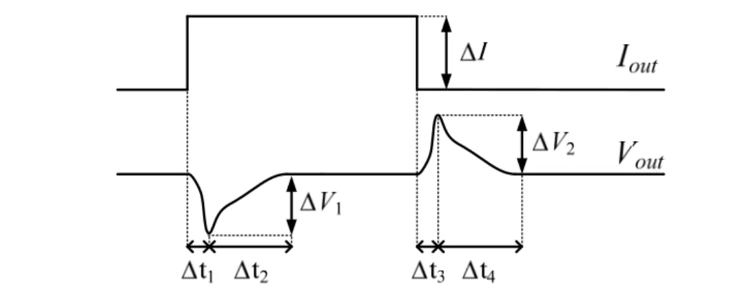
Transient Response is defined as a variation of output voltage when load current suddenly changes from one level to another level. The output voltage drops when load current steps up or increases when load current steps down since the additional or insufficient current supplied from the output capacitor. The transient response is a function of the bandwidth of DC-DC converter, output inductor, output capacitor, equivalent series resistance (ESR) of output capacitor and the load current as shown in Fig. 2.2. In past, this parameter is often ignored in industry. But in present age of high speed electronic manufactures, this parameter is more and more important because most kinds of electronic manufacture need to supply a large number of current in few microseconds even in few nanoseconds. If the DC-DC converter does not keep its output voltage which is supplied to electronic manufactures not change drastically in a big variation of load current, it will highly affect performance of electronic manufactures.
Fig. 2.2 Circuit diagram of the switching converter
Fig. 2.3 shows time characteristic of the transient response. During the time Δt1, a large current is pulled from the load, the finite bandwidth of the switching converter is too slow to provide enough output current to the load. Therefore, the output capacitor must compensate the difference between switching converter current and load current.
As a result, the voltage ΔV1 can be calculated as
1 1
O
I t
V I ESR
C
(2.7)
The time period Δt1 is mainly determined by the bandwidth of the switching converter.
Besides, a large output capacitor will keep on providing charges to the load and holding output voltage without transient spur. The sum of Δt1 and Δt2 is the “Recovery Time”
and it takes for the output to return within the specified regulation limits. ΔV1 is
“Deviation of Output Voltage” between two different load current ΔI. When the load steps down suddenly, the output voltage will jump. Before the inductor current is back to steady state, the excessive current charges the output capacitor. Therefore, ΔV2 can be calculated as
3 2
O
I t
V I ESR
C
(2.8)
The length of the time period Δt2 and Δt4 is dependent on the time required for pass power transistors, MP and MN, in Fig. 2.1 to charge or discharge the output capacitor, and it is also dependent on the phase margin of the whole circuit loop.
Fig. 2.3 The transient response of output voltage when a dynamic load is applied
2.2 Architecture of DC-DC Converters
A DC-DC converter is composed of a power stage and a feedback network. The power stage contains power transistors and an output filter. In the switched-mode DC-DC converter, the power stage contains power PMOS and NMOS transistors and the output filter which consists of an inductor L and a filtering capacitor C. Many feedback networks have been proposed and their goal in common is to provide a stable output voltage. These architectures will be discussed in detail as following.
2.2.1 DC-DC Buck Converter Operation
The buck converter, is a well-known converter that is capable of converting a higher voltage into a lower voltage. The switch produces a rectangular waveform Vs(t) as illustrated in Fig. 2.4. The voltage of Vs(t) is equal to the dc input voltage VIN when the switch is in position 1, and is equal to zero when the switch is in position 2. In practical, the switch is realized using power semiconductor devices, such as transistors and diodes, which are controlled to turn on and turn off as required to perform the function of the ideal switch. The switching frequency f , equals to the inverse of the
switching period Ts, generally lies in the range of 10 kHz to 10 MHz, depending on the switching speed of the semiconductor devices. The duty ratio D is the fraction of time that the switch spends in position 1, and is a number between zero and one. The complement of the duty ratio D’ is defined as (1-D).
Fig. 2.4 Buck converter (a) the switch in 1 (b) the switch in 2
Fig. 2.5 Steady-state output waveform V t s( )
The switch reduces the dc component of the voltage: the switch output voltage Vs(t) has a dc component that is less than the converter dc input voltage VIN. From Fourier analysis, we know that the dc component of Vs(t), as shown in Fig. 2.5, is given by its
average value VS
1 0S ( )
S S IN
S
V T V t dt DV
T
(2.9) So the average value, or dc component, of Vs(t) is equal to the duty cycle times the dc input voltage VIN. The output voltage is reduced from the input voltage by a factor of D.What remains is to insert a low-pass filter as shown in Fig. 2.4. The filter is designed to pass the average of Vs(t) but reject the components of Vs(t) at the switching frequency and its harmonics. The output voltage Vout is then essentially equal to the average of Vs(t). Fig. 2.6 depicts the control characteristic of the converter and the buck converter has a linear control characteristic. Note that the output voltage is less than or equal to the input voltage, since 0<D<1. Feedback systems are constructed to adjust the duty cycle D for regulating the converter output voltage. Inverters in digital controlled or error amplifiers in analog controlled could be built, in which the duty cycle varies slowly with time depending on feedback bandwidth.
Fig. 2.6 Output characteristic of buck converters
The conventional buck converter with inductor current and voltage waveforms shows in the Fig. 2.7. The transistor M1 is usually switched at high frequency to produce a chopped output voltage Vs. This is then filtered by the LC filter to generate a smooth load voltage Vout. When transistor M1 turns on, Vs=Vin, the voltage across the inductor
is:
L in out
V L di V V
dt (2.10) As a result, IL increases linearly. When transistor M1 turns off, the current through the inductor cannot instantaneously fall to zero, so the diode provide a return path for the current to circulate through the load. During this period, Vs=0, so the voltage across the inductor is:
L out
V L di V
dt (2.11) So IL decreases linearly. The peak-to-peak current ripple is:
on Vin Vout Vin T (1 )
I t D D
L L
(2.12)
Therefore, the maximum current and the minimum current are defined separately as:
max
min
2 2
out
out
V I
I R
V I
I R
(2.13)
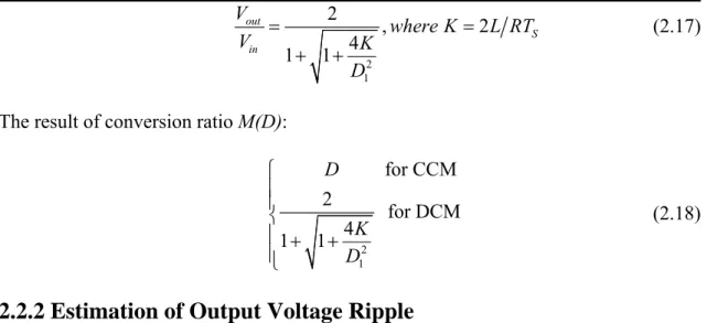
In Fig. 2.7(a), the continuous conduction mode (CCM) means that the minimum inductor current never falls to zero. When the minimum current falls to zero, it is discontinuous conduction mode (DCM) as shown in Fig. 2.7(b). In the steady state condition, the average voltage across an inductor over a complete is zero.
D1Ts D2TsD3Ts
Fig. 2.7 (a) The diagram and waveforms of continuous mode (b) The waveforms of discontinuous mode
In DCM,
1 2 3
( ) ( ) ( ) (0) 0
L in out out
V t D V V D V D
(2.14) Solution for conversion ratio yields
1
1 2
out in
V D
Conversion ratio
V D D
(2.15) From Fig. 2.7(b), the average inductor current is calculated:
1 2
0
1 1 2
1 1 1
( ) ( )
2
( )( )( )
2
TS
L peak S
S S
out S
in out
i t dt i D D T
T T
V D T
Average inductor current V V D D
R L
(2.16)Elimination of D2 from conversion ratio equation and average inductor current equation,
2 1
2 , 2
1 1 4
out S
in
V where K L RT
V K
D
(2.17)
The result of conversion ratio M(D):
2 1
for CCM 2 for DCM 1 1 4
D
K D
(2.18)
2.2.2 Estimation of Output Voltage Ripple
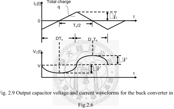
Considering the buck regulator of Fig. 2.8(a), the inductor current iL(t) with a dc component IL and linear ripple of peak magnitude ΔiL are shown in Fig. 2.8(b). It is impossible to build a perfect low-pass filter that allows the dc component to pass but completely removes the components at the switching frequency and its harmonics. So the low-pass filter must allow at least some small amount of the high-frequency harmonics generated by the switch to reach the output.
The output voltage switching ripple should be small in any well-designed converter, since the object is to produce a dc output. For example, in a computer power supply having a 3.3 V output, the switching ripple is normally required to be less than a few tens of millivolts, or less than 1% of the dc output.
Vin Vout L
Vout
L
i
LFig. 2.8 Buck converter (a) circuit (b) steady-state inductor current waveform In a well designed converter, in which the capacitor provides significant filtering of
switching ripple, the capacitance is chosen large enough that its impedance at the switching frequency is much smaller than the load impedance. Hence nearly all of the inductor current ripple flows through the capacitor, and very little flows through load.
As shown in Fig. 2.9, the capacitor current waveform IC(t) is then equal to the inductor current waveform with the dc component removed. The current ripple is linear, with peak value ΔiL.
IC(t)
t
DTs D゙Ts
0
i
LTs/2 Total charge
q
V
V
VC(t)
V
t
Fig. 2.9 Output capacitor voltage and current waveforms for the buck converter in Fig.2.6
From Fig. 2.9, by the capacitor relation Q=CV, the charge q is the integral of the current waveform between its zero crossings.
(2 )
q C V (2.19) 1
2 2
S L
q i T (2.20)
Substitution of equation (2.20) into equation (2.21), and solution for the voltage ripple peak magnitude ΔV yields
8 i TL S
V C
(2.21)
This expression can be used to select a value for the capacitance C such that a given
voltage ripple is obtained. In practical, the additional voltage ripple caused by the capacitor equivalent series resistance (ESR) must also be included. The voltage ripple with ESR is calculated as
( ) ( )
8 8
L S S
C L
i T T
V i t ESR i ESR
C C
(2.22)
In general, the ripple caused by first term “ESR” is much greater than caused by second term (Ts/8C). So consideration of ESR is essential for estimation of output voltage ripple in switching converter.
2.2.3 Feedback-Loop Stabilization
The simply feedback mechanism is illustrated in Fig. 2.10. The converter is composed of power stage and feedback network. The power stage contains a pair of switching elements, which consists of the power PMOS and NMOS transistors, and an output filter, which consists of an inductor and a capacitor. In feedback network, the difference of βVout which the output voltage is scaled down by resistor series and the reference voltage Vref is fed to the error amplifier. And then the output of the error amplifier and the ramp will pass through the comparator to define the duty cycle (PWM). The duty cycle controls the duration of the conducted time between the PMOS and the NMOS to achieve desired voltage such that the feedback is finished to regulate the output voltage The feedback system can be described as Fig. 2.11. The transfer function of the LC filter is defined as:
2
( ) 1
LC 1
H s
s LC
(2.23) The transfer function of the feedback network is defined as:
2
1 2
RR( ) H s R
R R
(2.24)
where T s3( )HLC( )s H sRR( ).
Fig. 2.10 The simply diagram of the PWM converter
Fig. 2.11 The transfer function of feedback system
It is fixed-amplitude pulse of adjustable turn-on ratio of the PWM modulator. Therefore, the transfer function of the PWM modulator is defined as:
2( ) P
T
T s V
V (2.25) where VT is amplitude of ramp waveform and VP is the amplitude of PWM signal. The HRR(s) and T2(s) do not effect on phase shift but they can decay the DC gain. As a result,
there is only error amplifier T1(s) that can provide gain boost to increase the total gain and influence phase for better phase margin.
Next, two types of the error amplifier will be introduced. The first is type II shown in Fig. 2.12 (a), and it has two poles and one zero. The transfer function is calculated as:
2 2 1
1 2
1 1 1 2 2
1 2
2 1
1 2
1 1 2 2 2
1
( )(1 )
1 ,
( )(1 )
V sR C
V sR C C sR C C
C C
sR C assume C C
sR C C sR C
(2.26)
The poles locate at the origin and the frequency
2 2
1
p 2
f R C , the zero locates at the
frequency
2 1
1
z 2
f R C . The frequency response is shown in Fig. 2.10(b) and (c). The
gain in the middle frequency is 2
1
R
R . As a result, appreciate resistors are chosen, and it can compensate the loss caused by the LC filter.
Fig. 2.12 Type II compensator with two poles and a zero
The second is type III, as shown in Fig. 2.13(a), and it has three poles and two zeros.
The transfer function is calculated as:
2 1 1 3 3
1
1 2
2 1 1 2 3 3 2
1 2
2 1 1 3
1 2 1 3
1 1 2 3 3 2 2
(1 )(1 ( ) )
( )(1 )(1 )
(1 )(1 )
, ,
( )(1 )(1 )
sR C s R R C V
V sR C C sR C sR C C
C C
sR C sR C
assume C C and R R
sR C C sR C sR C
(2.27)
The poles locate at the origin, the frequency 1
2 2
1
p 2
f R C and the frequency
2
3 3
1
p 2
f R C . The zeros locate at the frequency 1
2 1
1
z 2
f R C and the frequency
2
1 3
1
z 2
f R C . The gain and phase of this compensator is shown in Fig. 2.13 (b) and (c).
In summary, the maximum phase boost in type II compensator is 90 degrees, and in type III compensator is 180 degrees. According to stability and cost, the system will use the appropriate compensator to achieve desired performance.
Fig. 2.13 Type III compensator with three poles and two zeroes 2.3 Variable Frequency
In variable frequency techniques, there are four typical random switching methods discussed firstly. Then we will introduce a simplest method which is frequency hopping (FH). Since the main issue in this thesis focuses on the moment between different frequencies, the FH technique is a good choice to represent the main issue. Therefore, here uses the FH technique in following analysis,
2.3.1 Random Switching
There are four general random switching schemes for switched-mode DC-DC converters, including random-pulse-position-modulation (RPPM), random-pulse-width- modulation (RPWM), and random-carrier-frequency-modulation with fixed-duty-cycle (RCFMFD) and with variable-duty-cycle (RCFMVD), respectively. They are categorized by the random modulation of pulse which drives power transistors. The parameters of pulse are shown in Fig. 2.14. Tk is the duration of the kth cycle. εk is the delay time of the pulse. αk is the duration of the pulse in the kth cycle. dk which equals to αk/Tk is the duty cycle period of the switch turning on in the kth period. The amplitude of pulse is rail to rail of input voltage. Their operation will be addressed as following paragraphs.
Fig. 2.14 Switching parameters
RPPM is similar to the classical PWM scheme with constant switching frequency.
However, the position of the gate pulse or delay time εk is randomized within each switching period, instead of commencing at the start of each cycle. RPWM allows the pulse width αk to vary, but the average pulse width is equal to the required duty cycle.
RCFMFD exhibits randomized switching period Tk and constant duty cycle d=αk/Tk, while RCFMVD exhibits randomized switching period Tk and constant pulse width α.
With the aid of Fig. 2.15, the characteristics of the pulse g(t) in each scheme are summarized in Table 2.1.
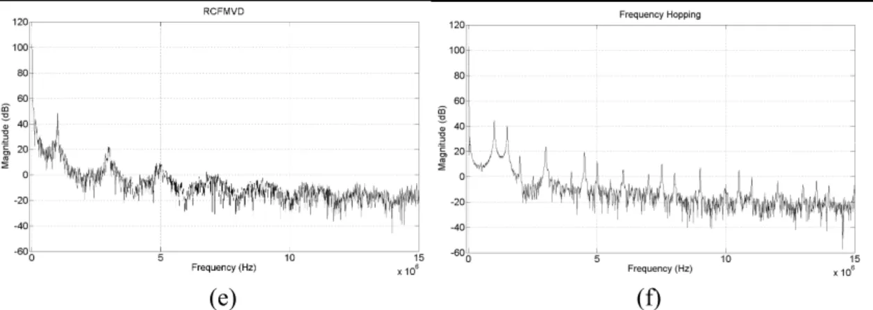
Fig. 2.15 Switching signal with randomized modulation (a)RPPM (b)RPWM (c)RCFMFD (d)RCFMVD (e)FH
Table 2.1 Characteristics of different random switching schemes Switching
schemes
Tk αk d=αk/Tk εk
Standard PWM
Fixed Fixed Fixed Fixed RPPM Fixed Fixed Fixed Randomized RPWM Fixed Randomized Randomized Fixed RCFMFD Randomized Randomized Fixed Fixed RCFMVD Randomized Fixed Randomized Fixed
FH Integer sets Integer sets Fixed Fixed
2.3.2 Frequency Hopping
Compared to random switching schemes, the frequency-hopping (FH) technique utilizes couples of fixed switching frequencies to achieve EMI-peak reduction. Using predictable frequencies relax the complexity of the filter. Its characteristic of the pulse is shown in Fig. 2.15(e). The spectrum results of these variable frequency techniques are shown in Fig. 2.16. Table 2.2 aids to understand each reduction for peak of EMI.
Another issue is the output voltage in time domain. In Fig. 2.17, these techniques have different phenomena in steady state. The reason is that the duty cycle varies in RPWM and RCFMVD.
(a) (b)
(b) (d)
(e) (f) Fig. 2.16 Output spectrum of different switching schemes
Table 2.2 Comparison of different switching schemes Switching
schemes
Peak of EMI (dB) Standard
PWM
50.77 RPPM 50.61
RPWM 50.4
RCFMFD 49.56 RCFMVD 48.56
FH 44.48
Fig. 2.17 Transient waveform of different switching schemes
Chapter 3 Proposed Architecture
3.1 Introduction
The inductor current average control (ICAC) is proposed in this paper. When using variable frequency techniques such as random switching or frequency hopping (FH), the inductor current ripple varies as the switching frequency changes. This variation of current ripple results in a transient ripple on the output voltage and undesired spur. In order to reduce this effect, this thesis discusses the best moment between different frequencies and how to implement. As aforementioned, the main issue focuses on the best moment between different frequencies and the FH technique adapts to this situation.
Therefore, it discusses the hopping moment in following analysis 3.2 Specification of DC-DC Buck Converter
The preliminary specification of DC-DC buck converter of this design is shown in Table 3.1. This work is used in portable devices to drive power amplifiers of RF circuits such as power-level tracking [14]. Therefore, the off-chip components must be small (LO>4.7μH and CO>10μF in conventional circuits) and the output current is determined by the power amplifier. Output voltage range is utilized to the standby mode and active mode in portable devices for saving power. Input voltage range is determined by the battery type. Switching frequency is usually fixed in typical PWM converters, but in spread spectrum methods such as frequency hopping (FH), it needs a particular frequency range.
Table 3.1 Specification of designed DC-DC buck converter.
Specification Parameters
Input voltage, VIN 3.6-5 V
Output voltage, vOUT 0.8-3.4 V Max. output current, IO 450 mA Output inductor, LO 1 μH Output capacitor, CO 1 μF Switching frequency, freq 2-3 MHz
3.3 System Architecture
In this chapter, the detailed operation of the chip will be discussed. The typical architecture is illustrated in Fig. 3.1. A PWM buck converter provides a regulated output voltage vOUT from an unregulated input voltage VIN. The PWM controller compares the ramp signal, vramp, with the output of the error amplifier to generate a square wave, vPWM, for voltage regulation. The gate driver drives the power transistors, MP and MN, with dead-time control to avoid a shoot-through current. The power transistors induce current passing a low pass filter which is composed with an inductor, LO, and a capacitor, CO to the load, IO. Note that the frequency of vramp determines the operation frequency and is able to change for hopping the frequency.
Fig. 3.1 Structure of a conventional PWM buck converter.
3.4 Inductor Current Average Control (ICAC)
As shown in Fig. 3.2, the FH technique with a lower frequency, f1, and a higher frequency, f2 [5] can avoid the energy concentrated on a single frequency at fnohop. Their magnitudes are 6dB down as two frequencies hopping in comparison with the magnitude at only one frequency. However, the converter output suffers transient ripples for several periods after hopping and it would result in an undesired spur at ftrans.
Fig. 3.2 Energy spread to multiple frequencies with the FH technique.
As shown in Fig. 3.3, in conventional PWM DC-DC converters [3], it assumes the frequency hopping at falling edge of vPWM for simplicity and random in practically. The inductor current, iL, increases during on duty cycle period, and decreases during off duty cycle period. In the example of Fig. 3.3, Ton,1 and Ton,2 represent the on duty cycle period of switching period at the low and high frequencies respectively. Toff,1 and Toff,2 represent the off duty cycle period of switching period at the low and high frequencies respectively. It reaches its peak/valley currents at the rising edge or the falling edge of vPWM. After the hopping moment, the average of the transient inductor current would be different from that of the steady-state inductor current, IL, due to the current continuity property of inductor. But, it would gradually approach IL when the inductor current is back to steady state. Therefore, the difference, ΔIL,trans, charges (or discharges) CO and generates transient ripple, Δvtrans on the output voltage. Its frequency response is the undesired spur at ftrans is dominated by LO and CO [15]. The undesired spur can be reduced by a larger capacitor but it pays a longer time to settle. Or, a larger inductor can be used but it occupies a larger area in the circuit.
An Inductor Current Average Control (ICAC) technique for FH structure is
proposed in this paper. As shown in Fig. 3.4, the best hopping moment could be chosen.
The best time length, TX, is calculated to correspond to the best hopping state, which maintains the same IL between the two frequencies. It modulates the off/on duty cycle period to be TX width. The calculated value of TX will be discussed in detail later. In the proposed hopping state, the output ripple voltage is improved by making the amount of charging close to the amount of discharging in the capacitor. If transient ripple on the output voltage is reduced, the undesired spur at ftrans in Fig. 3.4 is also reduced.
The best hopping state can be derived either in the off duty cycle period or the on duty cycle period. The proposed technique for FH from low to high and from high to low in these two different duty cycle periods will be discussed separately. Note that hopping in the off duty cycle period using ICAC is implemented in this chip.
Fig. 3.3 Transient waveforms of output voltage, inductor current and PWM signal in a conventional converter.
Fig. 3.4 Transient waveforms of output voltage, inductor current and PWM signal in the converter with the proposed ICAC technique.
3.4.1 Hopping in Off Duty Cycle Period
As mentioned before, there are two choices to hop, here discusses hopping in off duty cycle period with two parts. One is the frequency hopping from low to high, and another is the frequency hopping from high to low.
3.4.1.1 Hopping frequency from low to high
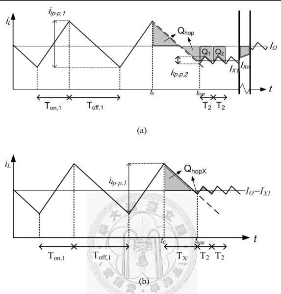
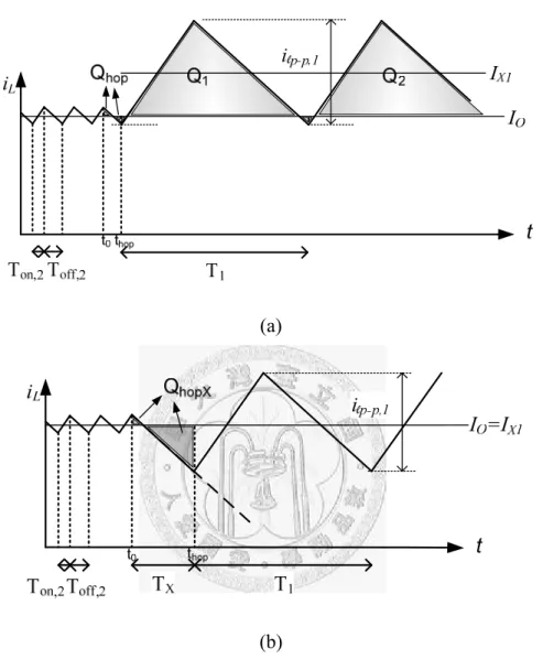
To reduce the complexity of transient response analysis, the loading is supposed to be a constant current source, IO as indicated in Fig. 3.1. Therefore, the load current IO is equal to the average or dc current IL.
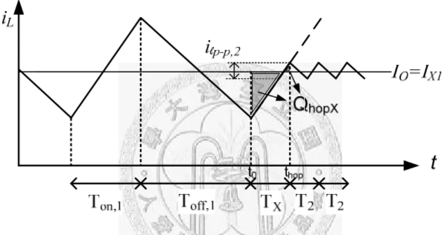
Q2
Qhop
T2 T2 Ton,1 Toff,1
Q1
(a)
(b)
Fig. 3.5 (a) Conventional and (b) proposed transient inductor current that hops frequency from low to high in off duty cycle period.
As shown in Fig. 3.5(a), the net charge on the capacitor, ΔQ, after t0 is
1 2
Q Q
hopQ Q
(3.1)
IXhop-IO
thop-t0 IX1-I TO
2 IX2-I TO
2
where IXhop is the average of transient inductor current from t0 to thop and IXi, i=1,2,… is the average of transient inductor current at the ith period of vPWM after t0. t0 is the time at which the inductor current is at its peak or valley and the capacitor voltage is at its dc value, VO. thop is the hopping moment. T2=Toff,2+Ton,2 is the period of vPWM after hopping.
The transient response can be separated into two parts, the charge in the hopping interval Qhop and total charge after hopping QT=Q1+Q2+…. Since settling time is longer than one period, Qhop is much smaller than QT.
hop T T
Q Q Q Q
(3.2) As illustrated in Fig. 3.5(a), QT is approximated with a triangular area. Its height is the difference between IO and IX1. Its width, TT, is the time from thop to the steady state.
1
- ,1 - ,2
(- )
1 1 1
2 2 2
1 -
T 2 X O T
lp p lp p T
Q I I T
i i T
(3.3)
- p- p,1 - p- p,2 IN
off
off,2 off,2 O
= i = i DV
m T T L
l l
(3.4) where ilp-p,1 and ilp-p,2 are the peak-to-peak values of the inductor current at low frequency and high frequency respectively. moff is the slope of the decreasing inductor current. D is the duty cycle.
Then, the conventional transient ripple on the output voltage can be obtained as
1 2
1 (1- )
( - ) 4
T IN
trans T
O O O
Q V D D
v T T T
C L C
(3.5)
where T1, T2 are the periods of the low and high frequencies respectively.
In order to minimize QT in (3.3), the best time TX of thop is proposed as follows. In Fig. 3.5(a), IX1 can be calculated as
1 1 - ,1 - 0 1 - ,2
2 2
X hop O lp p off hop lp p
I t I i m t t i
(3.6) According to (3.3), if IX1 equals IO, QT=0, most charge during transient settling time can be eliminated.
1 1
I + i + m t - t + i = I (3.7)