國 立 交 通 大 學
電信工程學系
碩 士 論 文
應用於數位電視寬頻調諧器之
三角積分調變頻率合成器
Delta-Sigma Frequency Synthesizer for
DTV Broadband RF Tuner
研究生:黃琳家
指導教授:洪崇智 博士
應用於數位電視寬頻調諧器之
三角積分調變頻率合成器
Delta-Sigma Frequency Synthesizer for
DTV Broadband RF Tuner
研 究 生:黃琳家 Student:Lin-Chia Huang
指導教授:洪崇智 Advisor:Prof. Chung-Chih Hung
國 立 交 通 大 學
電信工程學系
碩 士 論 文
A Thesis
Submitted to Department of Communication Engineering College of Electrical and Computer Engineering
National Chiao Tung University in Partial Fulfillment of the Requirements
for the Degree of Master
in
Communication Engineering October 2006
Hsinchu, Taiwan, Republic of China
應用於數位電視寬頻調諧器之
三角積分調變頻率合成器
學生:黃琳家
指導教授
:洪崇智
國立交通大學電信工程學系碩士班
摘
要
近年來,射頻積體電路(RFIC)技術迅速地發展演進。由於低成本以及低功 率消耗等優點,射頻積體電路在於無線通訊上的應用更是引人注目。在設計收 發機系統時的ㄧ大挑戰,便是在於如何合成所需要的任何本地震盪源(LO)訊 號。因此,頻率合成器隨即被發展出來以解決此種需求。 論文中提出分析ㄧ個整合於單一晶片,無須外掛其他被動元件的三角積分 調變除小數頻率合成器。此頻率合成器是以TSMC 0.18-微米互補式金氧半製程 製造,可以合成1.27 GHz 到 2.08 GHz 頻帶範圍,提供數位電視系統 135 個頻 道切換。模擬結果以及量測數據將會在內文中加以討論、解釋。 本論文主要區分為五部分。第一部分介紹數位電視系統相關知識。第二部 分探討鎖相迴路以及三角積分調變基本原理。我們將著重於電路設計概念以及 介紹一些現有的技術。第三部分呈現頻率合成器架構和組成方塊,包含修正後 的壓控振盪器、相位檢測器、電荷幫浦、迴路濾波器、可程式除頻器以及三角 積分調變器均會詳細地介紹。第四部分展示模擬及量測結果。最後,針對此次
Delta-Sigma Frequency Synthesizer for
DTV Broadband RF Tuner
Student:Lin-Chia Huang
Advisors:Dr.
Chung-Chih Hung
Department of Communication Engineering
National Chiao Tung University
ABSTRACT
Radio Frequency Integrated Circuits (RFIC) have been progressed rapidly in recent years. RFIC becomes attractive for applications in wireless communication due to its low cost and low power. One of the major challenges in the design of the transceiver system is the frequency synthesis of the local oscillator (LO) signal. Therefore, the frequency synthesizer is developed for this purpose.
In this thesis, a Delta-Sigma fractional-N frequency synthesizer in a single chip without any external discrete components is proposed and analyzed. The synthesizer was fabricated in TSMC 0.18µm CMOS process and can support all 135 channels of the DTV system from 1.27 GHz to 2.08 GHz. The simulation results and measurement data are discussed and explained in the content.
related knowledge of the DTV system. The second section discusses the basic principle of the Phase-Locked-Loop and Delta-Sigma modulation. We focus on the important circuit design concepts and existent techniques. The third section presents the architecture and components of a frequency synthesizer. In this section, a modified voltage-controlled oscillator, a phase-frequency detector, a charge pump, a loop filter, a programmable divider, and a delta-sigma modulator are all described in details. The fourth section shows our simulations and measurement results. Finally, a conclusion to this work is given. Suggestions for future works are recommended at the ending of this thesis.
Abstract
誌
謝
本論文能夠順利完成,首先要感謝我的指導教授洪崇智博士。感謝恩師在二 年碩士生涯中細心教導,不斷地指引學生正確的方向,使我對於研究學問的方法 及態度有更深一層的領悟,得以更快邁向成功的一步。若沒有老師的鞭策,本論 文絕對無法順利完成。另承蒙劉萬榮教授,黃淑絹教授,闕河鳴教授對本論文的 諸多指導與建議,使其能夠更趨完整與正確,在這裡謝謝每一位老師。還有,感 謝國家系統晶片中心提供先進的半導體製程,讓晶片的製作得以順利完成。 此外,感謝扶輪社提供高額獎學金,使我不必擔心經濟上的問題,能夠全心 投入於研究之中。感謝實驗室的莊誌倫、羅天佑、張家瑋、邱俊宏、李三益、楊 峻岳等諸位學長在這兩年的幫助與指導,讓我在求學路上能夠更加順利。感恩在 實驗室裡和我打拼了兩年的同學,林政翰、蔡宗諺、何俊達、楊家泰,謝謝你們 在研究及生活上的協助與鼓舞,使得我能夠堅持到最後一刻。還有許多學弟們, 為這實驗室帶來歡笑與活力,讓我們在苦樂中研究,歡樂中成長,也衷心的謝謝 你們。謝謝這一路支持我的女友,有了妳的陪伴,原本平淡無奇的生活頓時變得 多采多姿,讓我緊繃的情緒適時地獲得舒緩。 最後,最要感謝的是我的母親,含辛茹苦的一手拉拔我長大,給予我舒適的 環境讓我專心致力於學業上,追求自己的理想。您至高無上的愛,深植我心,千 言萬語都難以表達我內心的感動,希望您永遠健康、快樂。一路走來,得之於人 者太多,出之於己者太少。僅以此聊表心意,感謝所有曾經幫助過我的人。 黃琳家 于 交通大學電資大樓 710 研究室 九五年 十月
Table of Content
Table of Contents
Chapter 1
Introduction
...11.1 Motivation...1
1.2 Digital television Development ...2
1.2.1 Conventional Analog television………. 2
1.2.2 Introduction to Digital television………3
1.2.3 DTV in Taiwan………4
1.3 Digital television Broadband RF Tuner……….5
1.4 Thesis Overview………7
Chapter 2
Basic theories of Phase-Locked Loop
...92.1 Introduction to PLL...9
2.2 Architecture of Frequency Synthesizer………..11
2.3 Phase/Frequency Detector……….…..……..12 2.4 Charge Pump……….………...……...15 2.5 Voltage-Controlled Oscillator ……….………..16 2.5.1 Crystal Oscillators………. ……..………18 2.5.2 Ring Oscillators………....18 2.5.3 LC Oscillator………..…..19 2.6 Loop Filter……….19 2.7 Frequency Divider……….22
2.8 Noise Analysis of a PLL Synthesizer………22
2.8.1 Phase noise………...25
2.8.2 Spurs……….25
Table of Content
2.8.4 Noise of VCO……….…..26
Chapter 3
Principles of Frequency Synthesizers
………...283.1 Frequency Synthesizer Types and Comparison……….28
3.2 Fractional-N architectures……….29 3.2.1 Pulse swallowing………..29 3.2.2 Phase interpolating ……….……….31 3.2.3 Random jittering………...31 3.2.4 Delta-Sigma modulation………..32 3.2.5 Performance comparison………..33
3.3 Delta-Sigma Frequency synthesis……….34
3.3.1 Fundamental concepts………..34
3.3.2 First-order Σ∆ modulator………..35
3.3.3 High order Σ∆ modulator………..39
3.4 Mash implementations of Σ∆ modulator………40
Chapter 4
Frequency Synthesizers for DTV Tuner……….
434.1 Introduction………43
4.2 System architecture………43
4.3 Behavior Simulation………...45
4.4 Circuit Implementation………...48
4.4.1 Phase Frequency Detector……….48
4.4.2 Charge Pump……….49
4.4.3 Loop Filter……….52
4.4.4 Voltage-Controlled Oscillator………55
4.4.5 Programmable Frequency Divider………....60
Table of Content
4.5 Fractional-N Frequency Synthesizer System……….65
Chapter 5
Testing Setup and Experimental Results
...…695.1 Introduction………69
5.2 Experimental Results……….69
5.2.1 Prototype………...69
5.2.2 Test Setup………..70
5.2.3 Measurement Results………73
5.2.4 Conclusion and Discussion………...76
List of Figures
List of Figures
Fig. 1.1 Superheterodyne tuner………...………...6
Fig. 1.2 Double-Conversion tuner……..………...7
Fig. 1.3 Double-Conversion system spectrum………. 7
Fig. 2.1 Carrier recovery………..10
Fig. 2.2 Clock recovery……….……..……….……10
Fig. 2.3 Frequency demodulation………..……..….11
Fig. 2.4 The simplest diagram of frequency synthesizer ………12
Fig. 2.5 (a) Linear PFD architecture. (b) Operation of PFD ………13
Fig. 2.6 PFD state diagram………..14
Fig. 2.7 Ideal linear characteristic……….…………..14
Fig. 2.8 Conventional PFD………..14
Fig. 2.9 Dead zone problem……….15
Fig. 2.10 Charge pump………...15
Fig. 2.11 CP non-ideal effects………..16
Fig. 2.12 An oscillator crystal: (a) Symbol (b) Equivalent circuit ………18
Fig. 2.13 The simplest ring oscillator………..……….19
Fig. 2.14 Second order passive loop filter………20
Fig. 2.15 Open loop response Bode Plot……….21
Fig. 2.16 Third order filter………...21
Fig. 2.17 Output spectrum of (a) Ideal (b) Actual oscillator ………23
Fig. 2.18 Effect of phase noise in the (a) Receiver and (b) Transmitter …………24
Fig. 2.19 Spurs……….………25
Fig. 2.20 Noise transfer function of the PLL from input to output ………...25
Fig. 2.21 Bode plot of the normalized transfer function……….26
Fig. 2.22 Noise transfer function of the PLL from VCO to output………...27
Fig. 2.23 Phase noise performance of the VCO……….27
Fig. 3.1 Pulse swallowing fractional-N synthesizer……….30
Fig. 3.2 Sawtooth phase error………..30
Fig. 3.3 Amplitude compensation approach.………..31
List of Figures
Fig. 3.5 Delta-sigma modulation frequency synthesizer………33
Fig. 3.6 Σ∆ modulation structure and principle………..………35
Fig. 3.7 The equivalent model of a first-order Σ∆ modulator………. 35
Fig. 3.8 (a) Implementation (b) block diagram of a accumulator ………...36
Fig. 3.9 Realization of Σ∆ modulator………..………...36
Fig. 3.10 Basic structures of (a) second-order modulator (b) third-order modulator.. 40
Fig. 3.11 (a) Implementation and (b) block diagram of MASH 1-1-1……… 41
Fig. 4.1 the architecture of Σ∆ frequency synthesizer………44
Fig. 4.2 Behavior model of the fractional-N frequency synthesizer……….45
Fig. 4.3 Simulation results of fractional-N frequency synthesizer (a) Bode plot of open-loop response (b) transient response. ………...………..46
Fig. 4.4 PSD of Σ∆ modulator (a) 1st order (b) 2nd order (c) 3rd order………..……47
Fig. 4.5 Phase frequency detector ..………48
Fig. 4.6 The time diagram of the PFD………49
Fig. 4.7 (a) Basic charge pump (b) Modification for current reuse……….50
Fig. 4.8 Charge pump used in this synthesizer………...50
Fig. 4.9 The charge situation of the charge pump……….………51
Fig. 4.10 Dead zone simulation of PFD with CP………..………...………51
Fig. 4.11 the output voltage range of charge pump………52
Fig. 4.12 the third order filter……….……….52
Fig. 4.13 Basic design considerations of the third order filter………..53
Fig. 4.14 Bode diagram simulation of the PLL……….54
Fig. 4.15 Block diagram of ring oscillator with dual-delay paths………55
Fig. 4.16 Original delay cell of the ring oscillator………..56
Fig. 4.17 Tuning characteristic of the original ring oscillator………..56
Fig. 4.18 The proposed delay cell……….58
Fig. 4.19 The open drain structure………58
Fig. 4.20 Tuning characteristic of the proposed ring oscillator………..58
Fig. 4.21 Phase noise of the VCO………59
Fig. 4.22 The output swing with the PAD effect………59
Fig. 4.23 Tuning range of the VCO with corner model variation……….60
List of Figures
Fig. 4.26 SCL implementation of an AND gate combined with a latch function…61
Fig. 4.27 The simulation of divide-by-62 frequency divider……….62
Fig. 4.28 Second order Σ∆ modulator……….62
Fig. 4.29 Noise cancellation network………..63
Fig. 4.30 Realization of the noise cancellation network………64
Fig. 4.31 The flow chart of the modulation………64
Fig. 4.32 (a) VCO control voltage and (b) Out Spectrum when LO is 1.27GHz ….65 Fig. 4.33 (a) VCO control voltage and (b) Out Spectrum when LO is 2.08 GHz….66 Fig. 4.34 Physical layout of the Σ∆ frequency synthesizer……….67
Fig. 4.35 The PCB layout……….68
Fig. 5.1 Die microphotograph.………70
Fig. 5.2 LM317 regulator………71
Fig. 5.3 Bypass filter at the regulator output…….………71
Fig. 5.4 Measurement setup of the synthesizer………..72
Fig. 5.5 Photograph of (a) Waveform generator (b) Spectrum analyzer………..…72
Fig. 5.6 The testing PCB in the synthesizer………73
Fig. 5.7 The measured VCO transfer curve………...74
Fig. 5.8 The output spectrum of the synthesizer at 2.28 GHz with Span = 131.1 MHz and (b) Span = 76.53 MHz………...75
Fig. 5.9 The measured phase noise…..………...75
List of Tables
List of Tables
TABLE I Comparison between Different DTV Standards.………...4
TABLE II Total Performance comparison……….33
TABLE III Process corners simulation………..……60
TABLE IV Noise cancellation Network coding (A)………..63
TABLE V Noise cancellation Network coding (B)………..……….64
TABLE VI Performance of the Σ∆ frequency synthesizer..………..67
TABLE VII Comparisons between simulation and measurement……….……..74
Chapter 1
Introduction
1.1 Motivation
Television is the most important medium that educates, informs, and entertains the general public around the world. With the development of communication electronic, the demand for high-quality seeing and hearing information grows increasingly. Traditional television had been already difficult to satisfy customers, so digital television (DTV) technology was proposed to improve this problem. In recent years, DTV system has expanded maturely. Many countries such as America, Europe, Japan, have already advertised relative transmission standard and rules of application [1]. At the same time, Taiwan has also started the transition from analog to digital television.
DTV not only delivers distortion-free audio and video signals but also achieves much higher spectrum efficiency than analog television. DTV can also interface with other communication systems, digital media, and computer networks, making datacasting and multimedia interactive services possible [2][3]. In view of this, it is a key point of the ongoing digital leading toward the information society. A receiver or tuner must be needed in a digital television set to implement channel selection. Thus, it can be seen that a receiver plays an important role in our future digital broadcasting.
Frequency synthesizer is a essential function block in the receiver. It can provide a precise clock frequency to the tuner. By double conversion system, it can select the channel what we want. How to implement a frequency synthesizer by current technology will become a basilic study in the future. Based on this requirement, we use a fractional-N PLL with a second-order modulator to synthesize all frequency range that we need.
1.2 Digital television Development
1.2.1 Conventional Analog television
Traditional analog television is mainly divided into three independent transmission standards. They are NTSC (National Television System Committee), SECAM (Sequential Couleur Avec Memoire or Sequential Colour with Memory), SECAM (Sequential Colour with Memory), PAL (Phase Alternating Line). Besides Taiwan, many countries in the world has also adopted NTSC standard for a long time. This format has been in use from 1954. This technology is achieved by transmitting varying frequencies of radio waves. It uses 525 horizontal lines of picture resolution. This type of TV signal did have the flexibility to add some characteristics such as closed captioning, stereo sound, the second audio program feature, and the transmission of other data. Nevertheless, Analog television signals degrade over distance and are extremely susceptible to sources of interference. This means that some problems such as ghost images or snow may appear, even with expensive equipment and powerful transmitters.
1.2.2 Introduction to Digital television
Television is in the process of converting from analog to digital technology nowadays. Digital technology transmits in strings of 1’s and 0’s. Compared with analog signals, digital form is susceptible to signal loss over distance and is less probably to degrade due to interference. Therefore, digital signals are the preferred media of future transmission due to the simple fact that a 1 is still a 1 regardless of how strong the signal is or is not. In addition to these advantages, the digital signal can be compressed and store more information in less space.
The digital television standard is designed to transmit high-quality video, audio and ancillary data over a 6 MHz channel, which is the same bandwidth used for one analog NTSC channel today. The system is designed to reliably deliver about 19 Mbps (million bits per second) of data in a single terrestrial broadcast channel. DTV can carry standard definition television (SDTV) and high definition television (HDTV). HDTV encompasses six video formats, including the 1080-line interlaced (1080i) mode at either 24, 30 or 60 pictures per second, and the 720-line progressive (720p) format at the same picture rates. All these formats will have a wide-screen, 16:9, aspect ratio. This can be 2 to 3 times as many lines producing a higher picture density. The SDTV formats encompass 12 different versions of a 480-line signal-some progressive, some interlaced. The aspect ratio for the 480-line signal can be either the wide-screen, 16:9 format or the standard width, 4:3 format. SDTV has less resolution but allows the bandwidth of a DTV channel to be subdivided into multiple sub-channels. Broadcasters have the flexibility to select between offering a high definition picture and offering multiple programming options.
The technology of DTV will allow broadcasters to provide free television with CD-quality sound and movie-quality picture and manifold other enhancements.
DTV will also make the rapid delivery of large amounts of information services over your television set possible. Because DTV can free up valuable broadcast spectrum, it will be available for other information and communication services. However, it will depend on individual broadcasters to choose which services they will make available with DTV. Based on previous description, digital skills indeed afford a lot of benefits on DTV.
1.2.3 DTV in Taiwan
Today, the DTV specification development over the world mainly is divided into three segments. They are ASTC (Advanced Television Systems Committee), DVB (Digital Video Broadcasting), ISDB (Integrated Services Digital Broadcasting). Relevant comparisons between them are listed in Table I.
TABLE I Comparison between Different DTV Standards [6]
DVB-T ATSC ISDB-T
Audio MPEG1-layer2 AC-3 MPEG1-layer2
Image MPEG-2 MPEG-2 MPEG2
Bandwidth 6/7/8 MHz 6 MHz 5.6 MHz
Modulation COFDM 8VSB DQPSK/QPSK/16QAM
/64QAM/OFDM DVB-T is in operation in many countries around the world, but several countries follows the U.S. in adopting ATSC instead (Canada, South Korea, and Argentina). Japan is the only country to use ISDB. Taiwan terrestrial broadcasters started broadcasting digital programs in July 2004 using the DVB-T transmission system because of its superior features on mobile or portable reception, indoor reception, the support of country-wide single-frequency networks (SFN), compatible
characteristic with DVB-C and DVB-S, and so on.
In one way or another, we must all face the simple fact that the change of TV signals from analog to digital is avoidless. Currently there are 1 million DVB-T receivers being used in Taiwan, including car STB’s, in home STB’s and PC or Notebook PC DVB-T receivers. The government expected that they will recall the existing analogue TV signal and change into digital broadcasting in an all-round manner, when the DTV rating is up to 85% on January 1 , 2006. In the transition years, the government will ask for stations to convert their systems to the DTV standards and will allow them to broadcast analog and digital signals simultaneously. However, broadcasters will be forced to give up the analog portion of their signals at the end of the transition period. There are also provisions established that will extend the transition period. For example, analog signal will not cease until 85% or more of a given market owns a DTV capable television. Nowadays, Taiwan has not yet made a precise decision on an analogue switch off date but continues to go forward with Digital TV.
1.3 Digital Television Broadband RF Tuner
In order to watch digital television, there must be a receiver in the TV set to implement function of downconversion. Generally speaking, there are four types of receivers, comprising Superheterodyne Receiver, Direct-Conversion Receiver, Low-IF Receiver, Double Conversion Receiver. Most of the traditional TV have adopted “Superheterodyne Receiver” structure, but it was unsuited for portable products because of its huge volume. Fig. 1.1 shows the traditional Superheterodyne tuner.
Fig. 1.1 Superheterodyne tuner
For the sake of reducing the demand for tracking filter, more and more tuners are designed by Double Conversion structure, composed of frequency synthesizers, mixers, and low noise amplifiers, as shown in Fig. 1.2. The first local oscillator (LO) is synthesized by a PLL and controlled by a microprocessor. The second LO is a fixed reference oscillator. This type of tuner converts the entire input band of 50-860MHz up to a fixed first intermediate frequency (IF), that is above the highest input frequency of interest, and selects the desired channel by the RF saw filter. This process rejects the image of the downconversion. Then, the selected channel is down converted to the second intermediate center at 43.75MHz and passes through the second IF saw filter. Finally, the output signal feeds the next stage to demodulate DTV signal. The detailed spectrum is shown in Fig. 1.3.
Fig. 1.2 Double-Conversion tuner
Fig. 1.3 Double-Conversion system spectrum
1.4 Thesis Overview
This thesis comprises five chapters of which this introduction is the first. Chapter 2 begins with basic ideas of phase-locked loops as well as some important characteristics in a frequency synthesizer. The most important part describes the design concepts and every building block in a PLL.
In Chapter 3, we show several techniques to implement fractional-N PLL. The most significant part is the theorems of delta-sigma modulation. We also derive its analytic function to prove the abilities of randomization and noise shaping.
In Chapter 4, a completely integrated delta-sigma frequency synthesizer fabricated in 0.18µm CMOS 1P6M process is presented. We first introduce the architecture of the synthesizer and the behavior simulation in MATLAB. Then, every building block such as the phase frequency detector, the charge pump, the loop filter, the voltage-controlled oscillator, the programmable divider, and the delta-sigma modulator, are discussed and designed.
In Chapter 5, we present the testing environment, including the instruments and components on the print circuit board (PCB). The experimental results for the Σ∆ frequency synthesizer described in Chapter 4 will be presented.
Chapter 6 gives conclusions to this work, in which a delta-sigma fractional-N frequency synthesizer is designed and verified to be feasible. Suggestions for future works are recommended at the end of this thesis.
Chapter 2
Basic theories of Phase-Locked Loop
2.1 Introduction to PLL
Phase-locked loops are used widely in the modern system such as communications, command, telemetry, radar, time and frequency control, computer, and instrumentation systems. Today, it is rare to find a piece of electronic equipment that does not employ a PLL in some form. Take communications for instance, they can recover the carrier from satellite transmission signals, recover clock from digital data signals, synthesize exact frequencies for receiver tuning, perform frequency and phase modulation and demodulation, and reduce EMI effects.
A PLL circuit can make a particular system to track with another one. More definitely, a PLL synchronizes the output signal of an oscillator with a reference signal in frequency as well as in phase. When PLL is locked, the phase error between the reference signal and the oscillator,
s output signal is zero or remains constant.
Some examples are described as follows [6]:
1. Carrier recovery: In all applications related to coherent telecommunications, it is necessary to reconstruct a carrier reference from a noise-corrupted version of the received signal first. Fig. 2.1 shows a received signal vi consisting of bursts of a
sinusoid. When a burst occurs, a PLL can detect the error and then create a output signal vo to correct the phase.
Vi(t) Vo(t) t t ωi ωo Vi(ω) Vo(ω) ω ω ωo = ωi
Fig. 2.1 Carrier recovery
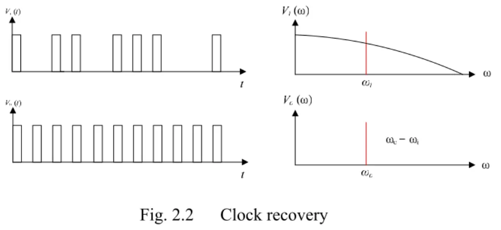
2. Clock recovery : A clock signal is need to be synchronized to a digital data signal vi in some application. As shown in Fig. 2.2, vi represents the data sequence
which is 1,0,1,1,0,1,1,1,0,0,1. Analyzing this data signal knows that there is a component at ωi, where 2π/ωi is the spacing between logic symbols. A PLL can lock
the oscillator frequency ωo to the ωi, producing the clock signal vo.
Fig. 2.2 Clock recovery
3. Frequency demodulation and Phase demodulation: Most FM receivers today adopt a PLL for frequency demodulation. If the bandwidth of the PLL is wide enough, the PLL output frequency ωo can track the input frequency ωi as it varies
according to the modulation. If the control voltage νc of the voltage control oscillator
(VCO) is proportional to ωo , it is also proportional to ωi. Consequently, νc is the
demodulated signal, as shown in Fig. 2.3. Similar concepts can be used for phase demodulation.
Fig. 2.3 Frequency demodulation
2.2 Architecture of Frequency Synthesizer
Frequency synthesizers play an crucial role in the field of communications. The frequency synthesizer was a system creating a set of frequencies what we need. Generally speaking, three common frequency synthesizer types can be distinguished: the direct synthesizer, the indirect or phase-locked synthesizer, and the table-look-up or digital synthesizer. Because the direct synthesizer is too bulky to integrate on a chip and the digital frequency synthesizer can not be used for high output frequencies, most synthesizers used in modern high frequency communication systems are of the phase-locked loop type.
A indirect synthesizer generates multiples of an accurate reference frequency. It is composed of five parts: a phase/frequency detector (PFD), a charge pump (CP), a loop filter (LF), a voltage-controlled oscillator (VCO) and a programmable frequency divider with a divider ratio N. The simplest form of this synthesizer is
shown in Fig. 2.4.
The operation of the PLL is as follows: the VCO output frequency (Fout) is
divided by N. The PFD compares the divided frequency (fdiv) with the reference
frequency (Fref), then it gives digital up or down signals, which is equal to the phase
difference between them, to control the CP. The CP would change the digital signals to the corresponding analog voltage signals. After that, the voltage signal is low-pass filtered by the loop filter, and is used to control the frequency of VCO. When PLL is locked, the phase of the divided output signal accurately tracks the phase of the reference signal. The phase-lock process forces fdiv and Fref to be equal. Finally,
we can obtain
Fout = N.Fref (2.1)
Fig. 2.4 The simplest diagram of frequency synthesizer
2.3 Phase / Frequency Detector
A PFD, which is usually built with a state machine with memory elements such as flip-flops, can monitor the difference between two input signals. Fig. 2.5 illustrates a common linear PFD structure using resettable DFFs and its operation diagram. If the reference signal leads the feedback signal, PFD will output an UP
signal with its pulse width proportional to the phase difference. However, if the reference signal lags the feedback signal, PFD will output a corresponding DN signal.
(a)
(b)
Fig. 2.5 (a) Linear PFD architecture (b) Operation of PFD
We could make a state diagram according to the operation of PFD, as shown in Fig. 2.6. Initially, outputs are both low. When one of the PFD inputs rises, the corresponding output becomes high. The state of the finite-state machine changes from an initial state to an Up or Down state. The state is held until the second input goes high, which in turn resets the circuit and returns the finite-state machine to the initial state. Fig. 2.7 illustrates that the characteristic of the PFD is ideally linear for the entire range of input phase differences form -2π to 2π.
Fig. 2.6 PFD state diagram
∆Φ
Fig. 2.7 Ideal linear characteristic
A conventional CMOS PFD is shown in Fig. 2.8. This PFD has large dead zone, which is shown in Fig. 2.9, in the phase characteristic at the equilibrium point, which generates a large jitter in locked state in PLL. Furthermore, the maximum speed is limited because of the total gate delay [7][8].
.
Fig. 2.9 Dead zone problem
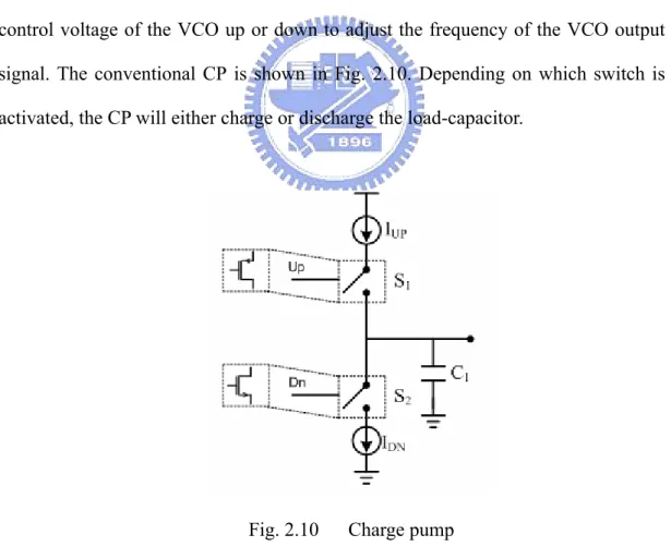
2.4 Charge pump
The charge pump (CP) is an analog circuit controlled by the PFD outputs. It generates phase error correction current pulses to the loop filter, in order to pull the control voltage of the VCO up or down to adjust the frequency of the VCO output signal. The conventional CP is shown in Fig. 2.10. Depending on which switch is activated, the CP will either charge or discharge the load-capacitor.
Fig. 2.10 Charge pump
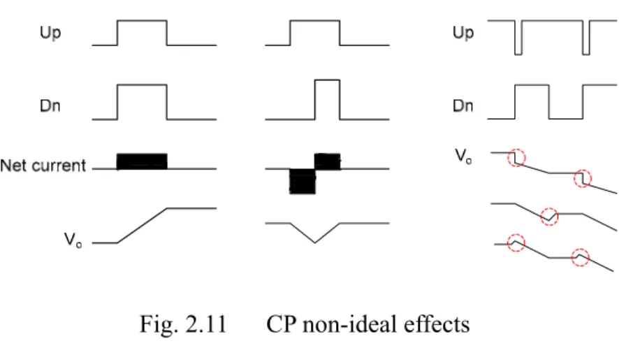
Because these switches consist of MOS transistors, they suffer from several non-ideal effects, such as mismatches, charge injection, clock feedthrough, and
charge sharing, giving rise to clock-skew and reference spurs in the output of PLL. Fig. 2.11 illustrates those effects on the output voltage.
Fig. 2.11 CP non-ideal effects
Subsequently, we discuss the PFD combined with CP. If the phase error between reference signal and feedback signal is ∆ , the charge or discharge current φ of the CP is Ip, the average error current in a cycle is Ie, then
2.5 Voltage-Controlled Oscillator
The voltage-controlled oscillator (VCO) operates at the highest frequency and usually determines the out-of-band noise of the frequency synthesizer. Different applications usually require different specification for the VCO. These requirements are often in conflict with one another, and therefore a compromise is needed. The most important specifications of the VCO are the tuning range, the power consumption, the phase noise, the tuning linearity, and the frequency
2 e p I φ I π ∆ = (2.2) 2 p e d I I K φ π = = ∆ (2.3)
- Tuning range: the VCO must be able to cover the complete required frequency band of the application, taking account of process variations.
- Tuning linearity: to simplify the design of the PLL, the VCO gain Kvco should be
constant.
- Frequency pushing: the dependency of the center frequency on the power supply voltage (in [MHz/ V]).
- Frequency pulling: the dependency of the center frequency on the output load impedance.
The output frequency (Fout) of the VCO is dependent on its control voltage
(Vcontrol). The relationship between them can be written as
, where Kvco (Vcontrol) is the VCO gain factor in [Hz/V] and ωout is the free running
frequency. The relationship of phase θo of the VCO signal with the control voltage
Vcontrol can be derived as
Dropping the first term of the integral, which is not dependent on Vtune, results in
After phase and frequency lock is achieved, Vcontrol is nearly constant, so the
dependency of Kvco on Vcontrol can be neglected. Taking the Laplace transform of (2.7)
yields
We will discuss the most often used oscillator types now.
ω
out=
ω
center+
(
K
vcoV
control)
i
V
control (2.4)( )
=
( )
o t out
t dt
θ
∫
ω
(2.5)
=
∫
(
ω
center+
(
K
vcoV
control)
i
V
control)
dt
(2.6)( )
=
(
)
o t
K
vcoV
controlV
controldt
θ
∫
i
(2.7)( )
o vco controls
K
V
s
θ
=
(2.8)2.5.1 Crystal Oscillators
The most stable oscillator is the crystal oscillator. The symbol and equivalent circuit is shown in Fig. 2.12. From it, we can derive that a crystal has two resonance modes. At series resonance frequency
ω
s , the impedance of the crystal becomesalmost zero. At parallel resonance frequency
ω
p , the impedance of the crystal isinfinite. The corresponding resonance frequencies
ω
s andω
p areSince Cp is much larger than Cs ,
ω
s andω
p are very close together. This is the reasonwhy crystal oscillators achieve very low phase noise. Their low noise and good stability let them the first choice for generating the reference signal in a frequency synthesizer .
Fig. 2.12: An oscillator crystal: (a) Symbol (b) Equivalent circuit
2.5.2 Ring Oscillators
The ring oscillator is one of the most popular oscillators for clock recovery circuits and integrated PLLs because it is simple and easy to integrate. The periodic signal is generated by a ring of inverters. They can be built of three or more inverters,
2 = 1 2 1 1 + 1 s p s s s s p L C L C C
ω
ω
⎛⎜⎜ ⎞⎟⎟ ⎝ ⎠ = i (2.9)is 1 / 2n·Td , where n is the number of inverters in the ring and Td is the delay of one
inverter. Fig. 2.13 shows the simplest ring oscillator. The tuning range is large. However, the phase noise is inferior,impeding its use in high-quality communication systems.
Fig. 2.13 The simplest ring oscillator
2.5.3 LC Oscillators
To improve the phase noise of the ring oscillator, the power consumption will become unacceptably high. The best way to overcome this problem is to utilize the LC oscillator. Since this structure uses high Q passive elements to be their loads, it is expected that it will have a pure spectrum. Generally speaking, the phase noise of LC oscillators is 20dB better than those of ring oscillators. Also high speed operation is achieved because of the simple working principle. Nevertheless, the biggest challenges are how to realize inductors and to reduce needed area.
2.6 Loop Filter
The loop filter provides the current-to-voltage conversion from the charge pump signal to the tuning voltage input of the VCO. The purity of the tuning voltage determines how the spectrum of the VCO output signal is. In consequence, most of the PLL’s specifications will be determined by the loop filter. In the loop filter, extra poles and zeros can be introduced in the open loop transfer function, which are used to set the noise and transient performance of the PLL. The standard second-order
passive loop filter configuration is shown in Fig. 2.14. The shunt capacitor C1 is used to mitigate discrete voltage steps at the control port of the VCO because of the instantaneous changes in the CP current output.
Fig. 2.14 Second order passive loop filter
Then we will discuss its design considerations by adding PFD and CP. The impedance of Fig. 2.14 is 1 2 2
1
//
( ) =
R
sC
Z s
C
⎛⎜⎜ ⎞⎟⎟ ⎝+
⎠ (2.10) 2 2 2 2 1 2 1 2 1 2 21
(
)
=
(
1)
(
)
1
(
)
z h pC R s
C R
K
s
s
s
s
C C s
C C
C C R
ω
ω
⎛ ⎞ ⎜ ⎟ ⎜ ⎟ ⎜ ⎟ ⎜ ⎟ ⎜ ⎟ ⎝ ⎠+
+
≡
+
+
+
+
(2.11) 2 21
zC R
ω
=
, 1 2 2 1 2 2 11
p zC
C
C
C C R
C
ω
=
+
=
ω
⋅
⎛
⎜
+
⎞
⎟
⎝
⎠
With this transfer function, we can easily draw the Bode Plot to observe its behavior and use the open loop gain bandwidth and phase margin to determine the component.
Fig. 2.15 shows its Bode plot. Typically, we locate the unity gain frequency
ω
tFig. 2.15 Open loop response Bode Plot
However, additional pole is often necessary for suppressing the reference spur. For this application, we place a series resistor and a shunt capacitor prior to the VCO for more attenuation of unwanted spurs. The recommended filter configuration is shown in Fig. 2.16. The added attenuation from the low pass filter is:
Besides, it is worthy to notice that the added pole must be lower than the reference frequency, in order to significantly attenuate the spurs, but must be at least 5 times higher than the loop bandwidth to keep system stable.
Fig. 2.16 Third order filter
(
)
2 3 3Attenuation = 20log
⎡⎢ω
refR C
1
⎤⎥⎣
+
⎦ (2.12) R2 C2 C1 C3 R3I
cpV
ctr2.7 Frequency Divider
Frequency dividers are used to synthesize a high frequency LO from a precise low frequency crystal oscillator. The output frequency fdiv equals the input frequency
fin divided by an integer number. From this information we could derive a model for
the divider in the phase domain.
The phase θin of the input signal is given by
and the instantaneous frequency of the input signal is
and the phase of the output signal can now be found as
2.8 Noise Analysis of a PLL Synthesizer
Apart from channel selection and frequency accuracy, there are several other aspects of frequency synthesizers which have an influence on the performance of a transceiver, like phase noise and reference spur.
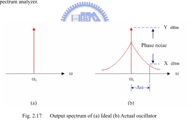
2.8.1 Phase Noise
A frequency synthesizer is expected to provide a pure spectral signal as shown in Fig. 2.17(a). There should be no unwanted frequency/phase modulation or
( ) = 2
p
sin 2
m int
π
f t
inθ
π
f t
θ
+
(2.13)( )
1
( ) =
+
cos 2
2
in p m m inst ind
t
f
t
f
f
f t
dt
θ
θ
π
π
=
(2.14)cos 2
=
instin
+
p m m divf
f t
f
f
f
N
N
N
θ
π
=
(2.15)( ) = 2
( )
= 2
+
sin 2
=
( )
div div p in m int
f
t dt
f
t
f t
N
N
t
N
θ
π
θ
π
π
θ
∫
(2.16)amplitude in the output spectrum because those undesired effect will reduce the channel selectivity and degrade the bit error rate of the receiver. However, the phase of the oscillation will fluctuate because of some noise at the frequency control input of the oscillator or the thermal noise of the resistors and transistors in the oscillator. The phase fluctuation forms “skirts” around the carrier in the frequency domain as shown in Fig. 2.17(b). So, the phase noise is developed in order to determine how the performance of a VCO is. The phase noise is characterized as the power ratio of the noise within an unit bandwidth at an offset ∆ω with respect to ωc to the carrier.
{ }
f
(
dBc Hz
/
) = (
X dBm Y dBm
)
(
) 10log(
RBW
)
L
∆
−
−
(2.17)where ∆f is the offset frequency from carrier and RBW is the resolution bandwidth of spectrum analyzer.
Fig. 2.17 Output spectrum of (a) Ideal (b) Actual oscillator
The phase noise has a great effect upon both the receiver and transmitter. As illustrated in the Fig. 2.18(a), if there is a large interference signal near the small desired signal and the LO exhibits phase noise, both the desired signal and the interference will be mixed down to the IF. However, both signals will suffer from
significant noise which is generated from the LO signal since the down-conversions is actually a convolution in frequency domain. If the powers of the interference signals are large, the signal-to-noise ratio (SNR) of the desired signal will be reduced. This effect is called “reciprocal mixing.” On the other hand, for the receiver, large-power transmitted signals with substantial phase noise will corrupt nearby weak signals. Therefore, the output spectrum of the LO must be extremely sharp to avoid being detected by mistake. Fig. 2.18(b) describes this appearance [13].
Fig. 2.18 Effect of phase noise in the (a) Receiver and (b) Transmitter
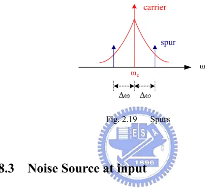
2.8.2 Spurs
In addition to phase noise, the oscillator can also be modulated by some fixed frequency noise due to the switching of other circuits in the synthesizer. Take current
switching noise in the divider and the CP at the reference rate for example, they may cause unwanted FM sidebands at the LO. Fig 2.19 illustrates this circumstance that two tones appear at the upper and lower sideband of the carrier. These tones are called “spurs”. It is similar to the case of phase noise that these spurious sidebands will also cause noise in adjacent channels and degrade the SNR of the desired signal.
Fig. 2.19 Spurs
2.8.3 Noise Source at input
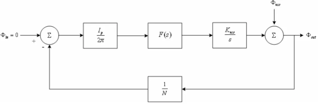
Fig. 2.20 shows the linear PLL model to analysis the input noise effect on the PLL output signal. The transfer function from Φin(s)to Φout(s) is derived as
Fig. 2.20 Noise transfer function of the PLL from input to output 1 ( ) ( ) 2 1 ( ) 1 ( ) 2
( )
vco out vco in K Ip F S s s N K Ip s F S s NH s
π π ⋅ ⋅ ⋅ Φ = Φ + ⋅ ⋅ ⋅=
(2.18)For simplicity, we use first-order loop filter to rewrite the above equation as
Fig. 2.21 shows Bode plot of the transfer function. The input phase noise is shaped by the low-pass characteristic of the second-order PLL. For the sake of reducing the phase noise in the output signal because of the input noise, it is expected to let the PLL bandwidth as narrow as possible.
Fig. 2.21 Bode plot of the normalized transfer function
2.8.4 Noise of VCO
The phase noise of the VCO can be modeled as Fig. 2.22. Similar to Eq. 2.19, we also use the first-order filter to derive the transfer function. It can be expressed as
2 2 2 1 1 2 2 1 1 2 1 2
( )
vco n n vco n n K sCR Ip s sC s N N K sCR Ip s s sC s NH s
π ξ ω ω ξ ω ω π + ⋅ ⋅ ⋅ ⋅ + = ⋅ + + ⋅ + + ⋅ ⋅ ⋅=
(2.19) where = and 2 2 2 p vco p vco n I K R I K C NC N π πω
ξ
=
2 2 2 1 1 1 2 1 2( )
vco n n s K sCR Ip s s sC s NH s
ξ ω ω π = + + ⋅ + + ⋅ ⋅ ⋅=
(2.20) where = and 2 2 2 p vco p vco n I K R I K C NC N π πω
ξ
=
Fig. 2.22 Noise transfer function of the PLL from VCO to output
Compared with the input noise, the VCO phase noise is shaped by a high-pass characteristic by the second-order PLL. If we want to reduce the VCO phase noise, we need to make the PLL bandwidth as wide as possible. In view of this, we can know there is a tradeoff in the bandwidth position. The optimum loop bandwidth depends on the application. However, it is common to increase the loop bandwidth since the dominant source of noise is usually the VCO in fully integrated frequency synthesizer. Fig. 2.23 shows the PLL effect on the VCO output spectrum.
Chapter 3
Principles of Frequency Synthesizers
3.1 Frequency Synthesizer Types and Comparison
Frequency synthesizers can traditionally be considered to be of two main forms. One is the integer-N frequency synthesizer, and the other is the fractional-N frequency synthesizer. For the integer-N synthesizer, its output frequency is always an integer multiple of the reference frequency. On the other hand, in the fractional-N frequency synthesizer the output frequency can be a fractional ratio of the reference frequency.The inherent limitation of an integer-N frequency synthesizer is that its frequency resolution is equal to the PLL reference frequency Fref. Fine frequency
resolution needs a small Fref and a correspondingly small loop bandwidth. Narrow
loop bandwidths are undesired due to inadequate suppression of VCO phase noise, long switching times, and susceptibility to noise. So, the fractional-N frequency synthesizer has been developed to solve this problem [13]. With the same channel spacing, the fractional-N frequency synthesizer can be designed with a higher loop bandwidth than the integer-N frequency synthesizer. Higher loop bandwidth results in faster frequency switching and thereby dynamic bandwidth techniques can be used more efficiently [14][15]. This will also relax the PLL requirements in terms of
synthesis solves the frequency resolution issue, but it also generates other unwanted problems.
3.2 Fractional-N architectures
When designing a fractional-N frequency synthesizer, we suffer from a trade-off between loop bandwidth, tuning bandwidth, frequency switching speed, and power consumption. There are four Fractional-N frequency synthesizer techniques: pulse swallowing, phase interpolation, Wheatly random jittering and Delta-Sigma modulation [16][17].
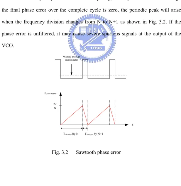
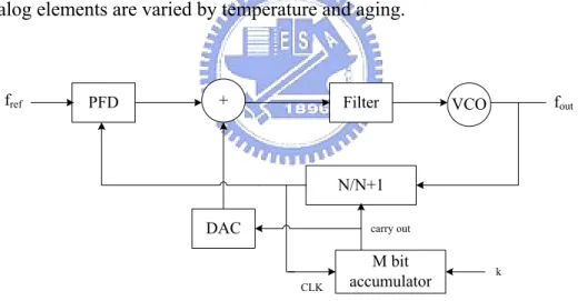
3.2.1 Pulse swallowing
Let us consider a pulse swallowing fractional-N synthesizer shown in Fig. 3.1. The condition of overflow in the accumulator is used to shift the divider modulus from n to n+1. For a M-bit accumulator, the average division factor N will be controlled by the accumulator input k as the following formula:
On every cycle of the divider output, k is added to the accumulator content X, so the new accumulator value would be X+k except the accumulator overflows. Then, the value assigned to accumulator is X+k-2M. In the condition of overflow, a carry output is generated to switch the divider modulus.
M
k
N = n +
PFD Filter VCO N/N+1 fout fref M bit accumulator CLK k carry out
Fig. 3.1 Pulse swallowing fractional-N synthesizer
The main problem of this operation is the phase error between the instantaneous frequency and the wanted frequency, at the phase detector. Although the final phase error over the complete cycle is zero, the periodic peak will arise when the frequency division changes from N to N+1 as shown in Fig. 3.2. If the phase error is unfiltered, it may cause severe spurious signals at the output of the VCO. 2 N π t Tdivision by N Tdivision by N+1 Wanted average divison ratio Phase error
3.2.2 Phase interpolating
The phase interpolation is a spur reduction skill to suppress the spurious tones as seen in the pulse swallowing approach. The technique uses amplitude compensation to the PFD output utilizing a digital to analog converter (DAC), as shown in Fig. 3.3. The accumulation of the phase of the fractional part is subtracted from the output of the PFD with that of the DAC. If the two signals exactly match, the phase error signal and output spurious are eliminated because fractional synthesis is reduced. However, the precision of the compensation directly rely on the DAC accuracy. Even if the system is well compensated during the production phase og the design, the compensation does not remain accurate as the characteristics of the analog elements are varied by temperature and aging.
PFD Filter VCO N/N+1 fout fref M bit accumulator CLK k carry out + DAC
Fig. 3.3 Amplitude compensation approach
3.2.3 Random jittering
This skill employs a random sequence generator to randomize the division modulus and so converts the output spurs to jitter [18]. Fig. 3.4 illustrates this concept. The comparator output is one bit in order to control the divider module.
This technique brings a main drawback that the output spectrum displays a 1/f 2 phase noise near the output frequency.
Fig. 3.4 Random jittering approach
3.2.4 Delta-Sigma modulation
Fig. 3.5 shows a Delta-sigma (Σ∆) modulation frequency synthesizer. The divider operates as the coarse quantizer, as only integer division ratios can be realized. By switching of the division between two or more integers, the average value of the division ratio is generated at the output of the frequency synthesizer. A Σ∆ modulator has the characteristic of noise shaping, so it can shape the phase noise resulting from randomization and quantization to a higher offset frequency. In this way, the SNR and dynamic range at the relevant frequency range is improved and the shaped quantization noise can be eliminated by filtering. However, it has a large power consumption and relatively high complexity.
PFD Filter VCO N/N+n fout fref Delta-sigma modulator CLK k carry out
Fig. 3.5 Delta-sigma modulation frequency synthesizer
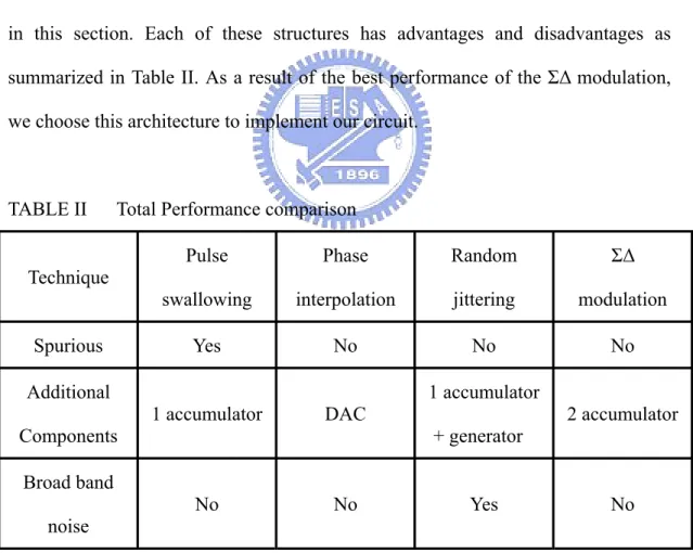
3.2.5 Performance comparison
A brief overview of different fractional-N frequency synthesizers is presented in this section. Each of these structures has advantages and disadvantages as summarized in Table II. As a result of the best performance of the Σ∆ modulation, we choose this architecture to implement our circuit.
TABLE II Total Performance comparison Technique Pulse swallowing Phase interpolation Random jittering Σ∆ modulation Spurious Yes No No No Additional
Components 1 accumulator DAC
1 accumulator
+ generator 2 accumulator Broad band
3.3 Delta-sigma frequency synthesis
Delta-sigma modulation technique was primarily used in over-sampling converters until Riley used the modulator noise shaping property to improve the random jitter and phase noise.
3.3.1 Fundamental concepts
Fig. 3.6(a) shows that a Σ∆ modulator consists of three components such as the integrator, the quantizer, and the differentiator. Their frequency response and power spectrum is shown in Fig. 3.6(b). In an analog to digital converter, the analog input propagates to an integrator followed by a quantizer working at a high sampling frequency compared to the Nyquist frequency. Then, the output of the quantizer is delivered to the differentiator. Fig. 3.6(c) illustrate the operation of this process, we can find that the Σ∆ modulator noise transfer characteristic is high pass in nature and results in very low in-band noise levels. So, the in-band quantization noise is alleviated and higher out-of-band quantization noise can be suppressed by the low pass loop filter.
In a fractional-N synthesizer, the input of the Σ∆ modulator is usually a digital word representing the wanted fractional value and the output of the modulator is a stream of integer numbers used to control the divider modulus. This stream forces the VCO output frequency to be fractional ratio of the reference frequency. Over time, the average if the Σ∆ modulator output converges to the desired fractional ratio.
1
1
(1−z−) (1−z−1)
Fig. 3.6 Σ∆ modulation structure and principle
3.3.2 First-order Σ∆ modulator
The equivalent model of a first-order Σ∆ modulator is shown in Fig. 3.7.
1
Z− Z−1
Fig. 3.7 The equivalent model of a first-order Σ∆ modulator
we can get the transfer function as follows:
Now, we consider an accumulator and its equivalent block diagram, as shown in Fig. 3.8.
1
(1
)
aFig. 3.8 (a) Implementation (b) block diagram of a accumulator
A transfer function of the accumulator can be derived as follows:
From Eq. (3.3), we find the output is a delayed version of the input with shaped quantization noise. Because the input is a constant, Eq. (3.2) and Eq. (3.3) are equal. We prove that the implementation of Σ∆ modulator can be achieved by a accumulator.
In order to know the effect of noise shaping, we incorporate the Σ∆ modulator in the PLL to control the divider modulus, as shown in Fig. 3.9.
X Y
~
÷N/N+1 Latch K b(t) overflow k bit Accumulator VCO PD X+Y LPF Fin Fout Fdiv + -1 [ ]. [ ] (1
) [ ]
a N z=
f z
+ −
z
−q z
(3.3)A discussion of the effects of quantization noise on the overall output, Fout ,
follows. Our first step is to evaluate the phase noise in Fdiv supposing an ideal VCO
at a fixed frequency. The instantaneous frequency of Fdiv(t), is determined by the
VCO frequency, Fout, and the instantaneous of division rate. The instantaneous
frequency division rate in the case of Σ-∆ modulated dual-modulus divider is given by n + b(t), where b(t) is the bit stream alternating between 0 and 1; hence
Then, the bit stream can be broke up into the desired dc value, K/M, and an additive quantization noise [19][20]. In the time domain the quantization noise is labeled
qe(t), giving
The normalized instantaneous frequency departure is defined as
Then,
If the rms spectral density of the quantization noise is labeled Sqe(f), then the
power spectral density of the normalized phase deviation will be given by ( ) ( ) out div F F t n b t = + (3.4) ( ) ( ) ( ) 2 out out div eff e e k F F F t K N q t n q t = ≡ + + + (3.5) ( ) 1 ( ) ( ) 1 ( ) 1 1
, where 1 for small
1+ in div e diff e in eff eff F F t q t F t q t F N N ε ε ε − = = − ≅ + ≅ − (3.6) ( ) 2 [ ( )] 2 ( ) 2 ( ) e in div in div in e eff t F F t dt F F t dt F q t N θ π π π = ⋅ − = ⋅ ⋅ = ⋅ ⋅
∫
∫
∫
(3.7) ' 2 in e( ) e eff F q t N θ = π⋅ ⋅ (3.8)According to Eq. (3.3)
Because the quantizer in first order Σ∆ modulator is one bit,
The power spectral density of the quantization noise through the quantizer can be described as follows:
( )
(
)
2 2 1 1 j f 2 s i n F i n i n z e f H f z F ππ
− = ⎛ ⎞ = − = ⎜ ⎟ ⎝ ⎠ (3.13)Combine Eq. (3.12) with Eq. (3.13), we can find its noise shaping ability
( )
1 2 2 s i n r a d / H z , 3 2 e i n q i n i n F f S f f F Fπ
⎛ ⎞ = ⋅ ⎜ ⎟ ≤ ⎝ ⎠ (3.14)Then from Eq. (3.9), we can get the final power spectral density of quantization noise is
( )
(
)
2 s i n 2 0 3 e i n i n e f f F f S f f F N f θπ
⎛ ⎞ = ⋅ ⎜ ⎟ ∝ ⋅ ⎝ ⎠ (3.15)However, from Eq. (3.15), we know that the noise un the output of VCO is flat, not the differential as we expected. In view of this, in order to obtain the noise shaping effectively, we must adopt the higher order Σ∆ modulator.
' 2 2 2 2 1 ( ) ( ) ( ) (2 ) 2 ( ) e e e e in q eff in q eff F S f S f S f f f N F S f f N θ θ π π π ⎛ ⎞ = ⋅ =⎜⎜ ⎟⎟ ⋅ ⋅ ⎝ ⎠ ⎛ ⎞ =⎜⎜ ⎟⎟ ⋅ ⋅ ⎝ ⎠ (3.9) 1 [ ]
(1
) [ ]
e z aq
= −
z
−q z
(3.10) 1 [ ] 12 a in z Fq
=
(3.11) 2 ( ) ( ) ( ) e a q q S f = H f ⋅S f (3.12)3.3.3 High order Σ∆ modulator
Based on the previous section, it is clear that implementing a fractional-N synthesizer with an accumulator known as a first-order Σ∆ modulator to control the divider is unwise. These shortcomings are greatly alleviated by implementing the division control with higher-order Σ∆ modulators. With this structure, the switching of the divider ratio is randomized, such that the spurious signals are no longer present in the output signal of the synthesizer. Fig. 3.10 (a) shows the second-order Σ∆ modulator and Fig. 3.10 (b) shows the third-order Σ∆ modulator. By principles of the superposition, we can easily know their outputs which the quantization noise is reduced more through noise shaping.
Second-order: Third-order: 1 1 1 z− − 1 1 1 z− − 1 z− (a) 1 2 Output = Input + (1qa −z− ) (3.16) 1 3 Output = Input + (1qa −z− ) (3.17)
1 1 1 z− − 1 1 1 z− − 1 z− 1 1 1 z− − (b)
Fig. 3.10 Basic structures of (a) second-order modulator (b) third-order modulator
3.4 Mash implementations of Σ∆ modulator
Higher-order delta-sigma modulators improve the noise shaping characteristic, even so, they are not always stable because there are several feedback loops in the system. Fortunately, this problem was solved in the structure referred as Multistage Noise Shaping Technique (MASH) [21][22][23].
The MASH or cascade 1-1-1 Σ∆ modulator is depicted in Fig. 3.11(a). The MASH modulator consists of a cascade of first-order modulators and of a combiner stage. Fig. 3.11(b) shows the block diagram of the MASH 1-1-1. The operation of the modulator is as follows: each subsequent first-order modulator performs a quantization operation on the quantization error from the previous stages; the combiner stage, on its turn, realizes a noise shaping operation on the output signals from the first-order modulators. The math equation description is as follows:
So, the output of third-order modulator is: 1 1( ) . ( ) (1 ) a1 N z = f z + −z q− (3.18) 1 2( ) a1 (1 ) a2 N z = −q + −z q− (3.19) 1 3( ) a2 (1 ) 3 N z = −q + −z q− (3.20)
X Y Latch K X+Y X Y Latch X+Y X Y Latch X+Y Latch + + X Latch + + b[n] C C C C1 C2 C3
-(a) + 1 1 1 z− − + + 1 z− .f(z) qa1(z) + 1 1 1 z− − + + 1 z− qa2(z) _ + 1 1 1 z− − + 1 z− qa3(z) _ 1 1 z− − + 1 1 z− − + _ _ _ - qa1(z) - qa2(z) N1(z) N2(z) N3(z) Nf(z) (b)Fig. 3.11 (a) Implementation and (b) block diagram of MASH 1-1-1
1 1 2 1 2 3 1 3 3 ( ) ( ) (1 ) ( ) (1 ) ( ) . ( ) (1 ) f a N z N z z N z z N z f z z q − − − = + − + − = + − ⋅ (3.21)
Similar to first-order Σ∆ modulator, we can also change the noise transfer function to H(f) = ( 1-z-1 )3 and get the final power spectral density of output noise.
( )
(
)
2 6 4 1 6 s i n 3 e i n i n e f f F f S f f F N f θπ
⎛ ⎞ = ⋅ ⎜ ⎟ ∝ ⋅ ⎝ ⎠ (3.22)According to Eq. (3.22), we find that the output power spectral density is now proportional to f 4, showing that the quantization noise is suppressed in the signal band. Through the process of the derivation, we can conclude that the for ith order Σ∆ modulator the power spectral density of the phase noise is [24]
( )
(
)
2 2 2 2 s i n 1 2 e i i n i n e f f F f S f r a d H z F N f θπ
⎡ ⎛ ⎞⎤ = ⋅ ⎢ ⎜ ⎟⎥ ⋅ ⎣ ⎝ ⎠⎦ (3.23)Chapter 4
Frequency Synthesizers for DTV Tuner
4.1 Introduction
Today,s high-performance RF frequency synthesizer are often required: (1) to have smooth transition among channel intervals; (2) to have low phase noise and frequency variation; (3) to work over a wide frequency range which can cover the desired range; (4) to have an integrated loop filter on the chip. In the previous chapters we discussed system level design issues of a frequency synthesizer. Based on the knowledge, we will implement a Σ∆ frequency synthesizer for a DTV broadband RF tuner. This synthesizer is fabricated in a 0.18µm standard CMOS technology. Provided a 36MHz input reference signal and several bits digital codes, the circuit can generate a frequency tuning range from 1.27 to 2.08 GHz with 6 MHz channel bandwidth.
4.2 System architecture
Fig. 4.1 shows this Σ∆ frequency synthesizer. It consists of phase frequency detector (PFD), charge pump (CP), voltage controlled oscillator (VCO), loop filter (LP), programmable divider, and Σ∆ modulator. The specification of every component must be designed with extreme care. The PFD must operate correctly to
distinguish phase error and frequency error, the filter must provide an optimum compromise in output noise, switching speed, and frequency settling. In addition to these, the VCO must be of high quality and the programmable divider should work at high speed.
Fig. 4.1 the architecture of Σ∆ frequency synthesizer
In the Fig. 4.1, we choose the second-order Σ∆ modulator to realize modulus control. When the output of the Σ∆ modulator is -1, 0, 1, and 2, we select the modulus of the divider as N+1, N, N-1, and N-2 respectively. Thus, a fractional division ratio from n fref to (n + 1) fref is achieved as known in previous chapters.
We use 7 bits accumulators to construct the modulator due to the minimum frequency resolution.
4.3 Behavior simulation
simulations can be made with SIMULINK to test and verify transient response and system parameters rapidly. The behavior model of the frequency synthesizer is implemented in SIMULINK as shown in Fig. 4.2. The behavior simulation results of the system are shown in Fig. 4.3 and Fig. 4.4.
Fig. 4.2 Behavior model of the fractional-N frequency synthesizer
(b)
Fig. 4.3 Simulation results of fractional-N frequency synthesizer (a) Bode plot of open-loop response (b) transient response
20dB/dec
40dB/dec
60dB/dec
4.4 Circuit Implementation
4.4.1 Phase Frequency Detector
A common drawback for some phase frequency detector is a dead zone in the phase characteristic at the equilibrium point. The dead zone generates phase jitter because the control system does not change the control voltage when the phase error is within the dead zone. This influence can be improved by increasing the precision of the PFD. To reduce the dead zone and to overcome the speed limitation, we choose the dynamic phase frequency detector shown in Fig. 4.5 [25]. Compared with the conventional PFD, the transistor numbers are decreased to 12 and thus possesses smaller parasitic inherently. According to the phase difference between both input signals, UP is used to increase and DN is used to decrease the frequency of the output signal. Fig. 4.6 simulates its operation situation.