This content has been downloaded from IOPscience. Please scroll down to see the full text.
Download details:
IP Address: 140.113.38.11
This content was downloaded on 28/04/2014 at 07:50
Please note that terms and conditions apply.
Improvement of Polysilicon Oxide Integrity Using NF3-Annealing
View the table of contents for this issue, or go to the journal homepage for more 2000 Jpn. J. Appl. Phys. 39 L562
(http://iopscience.iop.org/1347-4065/39/6B/L562)
Jpn. J. Appl. Phys. Vol. 39 (2000) pp.L562–L563 Part 2, No. 6B, 15 June 2000
c
°2000 The Japan Society of Applied Physics
Improvement of Polysilicon Oxide Integrity Using NF
3-Annealing
Wen Luh YANG, Ming Sun SHIEH1, Yu Min CHEN, Tien Sheng CHAO2, Don-Gey LIUand Tan Fu LEI1
Institute and Department of Electrical Engineering, Feng Chia University, Taichung, Taiwan, R.O.C. 1Institute and Department of Electronics, National Chiao Tung University, Hsinchu, Taiwan, R.O.C. 2National Nano Device Laboratories, Hsinchu, Taiwan, R.O.C.
(Received April 7, 2000; accepted for publication May 19, 2000)
We report a method to improve the polysilicon oxide integrity by using NF3-annealing. Incorporating with stronger Si–N
and Si–F bonds at the polysilicon/ polyoxide interface, significant improvements are found in terms of roughness, breakdown strength, charge-to-breakdown, and stress-induced-leakage-current.
KEYWORDS: polyoxide, NF3-annealing, nitrogen, fluorine, SILC
L562
1. Introduction
For nonvolatile memories such as erasable-programmable read-only memory (EPROM), electrical-erasable program-mable read-only memory (EEPROM), and Flash, thermal ox-ides grown on n+polysilicon (polyoxides) have been used as the interdielectrics. Requirements of the polyoxides include low leakage current and high electric breakdown field (Ebd)
to achieve a long charge retention time. However, polyox-ides exhibit lower Ebd and higher leakage current than
ox-ides grown on single crystal silicon due to surface rough-ness caused by the enhanced oxidation at polysilicon grain boundaries. Recent studies show that the reliability of MOS and polyoxide capacitors can be improved by introducing proper amounts of fluorine.1–3)It also reported that the N2
O-grown and N2O-annealing polyoxides have better electrical
performance than O2-grown polyoxide, which attributes to
the nitrogen incorporation at the polysilicon/polyoxide inter-face.4, 5)Therefore, in this paper, NF3-annealing is proposed
to achieve the advantages of both nitrogen and fluorine si-multaneously. By using optimized NF3 flow-rate, it can be
expected to improve the polyoxide integrity. As compared to the ion-implantation, this method provides a low cost and high throughput for mass production.
2. Experimental
The n+-polysilicon/polyoxide/n+-polysilicon capacitors were fabricated on the p-type (100) silicon wafers. First, a 100 nm-thick buried oxide was thermally wet oxidized at 1000◦C. Then the polysilicon layer (bottom polysilicon) with a thickness of 300 nm was deposited and subsequently doped with POCl3 at 875◦C to obtain a sheet resistance of 40–
60Ä/¤. The p-glass was stripped off and then an 83 Å poly-oxide was grown at 900◦C in dilute (N2+ O2) ambient. After
that, a 300 nm-thick top polysilicon layer was deposited, fol-lowed by annealing in the diluted NF3 gas. Samples were
annealed in NF3at 600◦C with pressure of 260 mTorr for
dif-ferent time, 10 to 30 minutes in a low-pressure chemical-vapor-deposition (LPCVD) system. After optimization, the flow rates for N2 and NF3are set at 200 and 3 sccm,
respec-tively. Then top polysilicon was doped by POCl3 as the n+
-polysilicon gate electrode at 875◦C for 1 hour. After defin-ing the top gate pattern, a passivation oxide was deposited by plasma enhanced chemical vapor deposition (PECVD) and contact holes were opened. Finally, Aluminum was sputtered, patterned, and sintered at 350◦C for 40 minutes.
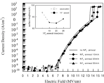
Fig. 1. The J-E characteristics of polyoxides with/without NF3 annealed for positive top-gate bias. The inset is surface roughness for these four samples.
3. Results and Discussion
Figure 1 shows curves of current density vs electric field. The electric field is defined as Vg/Tox, where Vg is the gate
voltage. The breakdown field, Ebd, increases with the
in-troduction of NF3-annealing, which reaches a maximum of
15 MV/cm for 20 minutes case. The inset in Fig. 1 shows the root-mean-square roughness measured by the atomic force microscope (AFM) of bottom polysilicon with different NF3
-annealing time. The value of surface roughness decreases as introduction of NF3and reaches to a minimum for 20-min
an-nealing. These results show that 20-min annealing is the opti-mized condition to obtain the smoothest surface of the bottom polysilicon, and results in a highest Ebdin return. For a longer
annealing time, i.e., 30-min, excessive fluorine and/or nitro-gen atoms break the Si–O–Si bonds and create non-bridging oxygen defects. Figure 2 shows gate voltage shift under con-stant current stressing at 100µA/cm2for these four samples. NF3-annealing samples show a smaller charge trapping-rate
than control sample. This implies NF3-annealing samples
have better immunity to electron trapping than control. As considering the reliability of polyoxide in nonvolatile memories, charge-to-breakdown (Qbd) is to guaranty long
read/write cycles. In the conventional polyoxide fabrication, Qbdvalues are very small (in the range of 0.01 to 0.1 C/cm2)
due to surface roughness and non-uniform polyoxide thick-ness. Figure 3 shows the Qbd for these four samples. With
NF3 treatments, Qbd increases significantly. Besides the
im-provement on roughness as mentioned in Fig. 1, the improved integrity is also due to incorporation of nitrogen and fluorine atoms which relax the interface stress.2, 4)It is found that Qbd
greater than 1 C/cm2 can be obtained as NF3 annealing time
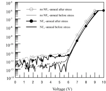
is larger than 20-min. Finally the stress-induced-leakage-current (SILC) was investigated. Mechanism of SILC could be explained by the stress-induced weak sports with a low-ing barrier height, the trap-assisted tunnellow-ing by the neutral electron trap filling and emptying, and the positive charge assisted tunneling.6–8) The fresh and the after stressed I –V
curves are shown in Fig. 4. It is seen that the SILC of the NF3-annealing sample was smaller than that of the control
sample. Once again, the stronger Si–F and Si–N bonds at
the polysilicon/polyoxide interface resulting from the NF3
an-nealing made polyoxides less vulnerable than the control sam-ple under the electrical stressing. In this study, all samsam-ples were measured with the positive-gate bias and the results of the negative-gate bias were similar to those obtained from the positive-gate bias.
4. Conclusions
NF3-annealing method had been demonstrated to improve
the polyoxide integrity. The breakdown field up to 15 MV/cm and charge-to-breakdown more than 1 C/cm2can be obtained using NF3-annealing. Incorporating with stronger Si–N and
Si–F bonds at the polysilicon/polyoxide interface, significant improvements are found in terms of roughness, breakdown strength, charge-to-breakdown, and stress-induced-leakage-current.
Acknowledgement
The authors would like to express thanks for the financial support of the Feng Chia University through the contract of FCU-RD-88-01. The partial financial support of the National Science Council of the R.O.C. (NSC-89-2215-E-035-010) is also acknowledged.
1) K. P. MacWilliams, L. F. Halle and T. C. Zietlow: IEEE Electron Device Lett. 11 (1990) 3.
2) H. N. Chern, C. L. Lee and T. F. Lei: IEEE Electron Device Lett. 15 (1994) 181.
3) P. Chowdhury, A. I. Chou, K. Kumar, C. Lin and J. C. Lee: Appl. Phys. Lett. 70 (1997) 37.
4) C. S. Lai, T. F. Lei and C. L. Lee: IEEE Trans. Electron Devices 43 (1996) 326.
5) J. H. Klootwijk, H. H. Weusthof, H. V. Kranenburg, P. H. Woerlee and H. Wallinga: IEEE Electron Device Lett. 17 (1996) 358.
6) P. Olive, T. N. Nguyen and B. Ricco: IEEE Trans. Electron Device 35 (1988) 2259.
7) S. H. Lee, B. J. Cho, J. C. Kim and S. H. Choi: IEDM Tech. Dig. (1994) 605.
8) D. J. Dumin and J. R. Maddux: IEEE Trans. Electron Devices 40 (1993)
986.
Fig. 3. The Weibull plots of the charge-to-breakdown for NF3-annealing polyoxide in different time at room temperature of 25◦C. The stress current density is 10 mA/cm2.
Fig. 2. The curves of gate voltage shifts versus stress time under a constant current stressing at 100µA/cm2.
Fig. 4. The fresh and stressed I -V curves of the stress-induced-leakage-current (SILC) for samples without NF3-annealing and the 20-min. NF3-annealing. The injected charge density is 0.05 C/cm2.