國立交通大學
電子物理學系
碩士論文
表面形態及結晶條件對薄膜電晶體與非揮發性
記憶體之影響
The Impact of Morphology and Crystallization Condition on
Thin Film Transistors and Nonvolatile Memories
研 究 生:劉劭軒
指導教授:趙天生 博士
表面形態及結晶條件對薄膜電晶體與非揮發性
記憶體之影響
The Impact of Morphology and Crystallization Condition
on Thin Film Transistors and Nonvolatile Memories
研究生:劉劭軒 Student : Shao-Xuan Liu
指導教授 :趙天生 博士
Advisor : Dr. Tien-Sheng Chao
國立交通大學
電子物理所碩士班
碩士論文
A Thesis
Submitted to Department of Electronphysics College of Science
National Chiao Tung University
in Partial Fulfillment of the Requirements
for the Degree of Master of Science in Electrophysics
June 2012,
Hsinchu, Taiwan, Republic of China.
中華民國 一百零一 年 六 月
I
表面形態以及結晶條件對薄膜電晶體與非揮發性記憶體之影響
研究生:劉劭軒 指導教授:趙天生 博士國立交通大學
電子物理研究所碩士班
摘要
近年來非揮發性記憶體的應用已遠超於任何人的想像, 像是個人
電腦、邏輯運算幫手以及各式各樣的電子攜帶式產品。另一方面,為
了成功實現系統整合面板(SOP)顯示器,提升 LTPS-NVSM 的品質當為首
要任務。然而,在 LTPS-NVSM 中,仍舊缺乏探討通道結晶條件對於記
憶體品質的影響的研究。基於此因,在本論文中我們將完整的探討表
面形態以及結晶條件對於薄膜電晶體以及非揮發性記憶體之影響。
首先,我們使用熱氧化製程製備了不同的表面粗糙度,並且探討
不同表面粗糙度對於寫入、抹除效率的影響。我們也發現了電晶體的
電性(如載子遷移率、臨界電壓以及漏電流)與表面粗糙度有很強烈的
相依性。此外我們發現通道厚度以及結晶溫度將會導致晶粒尺寸與缺
陷密度的差異,也因此影響了電晶體與記憶體的電性。通道厚度較厚
的元件提升了元件效能,卻導致較高的漏電流;而結晶溫度低的元件
(580
°C),拜能夠結晶出較大的晶粒所賜,展現了優越的電性。
II
另一方面,在本文中我們也探討了關於不同表面形態與結晶條件
對於記憶體的各種種類之可靠度問題,包含了 retention、閘極干擾(gate
disturbance)以及汲極干擾(drain disturbance)。
III
The Impact of Morphology and Crystallization Condition on Thin Film
Transistors and Nonvolatile Memories
Student: Shao-Xuan Liu Advisor: Dr. Tien-Sheng Chao
Institute of Electrophysics
National Chiao Tung University
Abstract
Recently, the applications of the nonvolatile memory device have gone far beyond anyone else such as computer, personal digital assistant, and electronic portable equipment. On the other hand, to realize system-on-plane (SOP) display, the important task is to improve LTPS-NVSM. However, the impacts of the poly Si channel condition on NVSM are missing. As the result, this dissertation studies the impacts of morphology and crystallization condition on thin film transistors and nonvolatile memory.
First, the roughness generated by thermal oxidation conditions was systematically reviewed for the nonvolatile memory P/E efficiency. Also, the mobility, threshold voltage, and leakage current exhibit a strong dependence on roughness. Moreover, we find the channel thickness and crystallization temperature altering the grain size and trap density, resulting in the different electrical characteristics of nonvolatile memory and transistors. Thicker channel devices enhance performance but case higher leakage current. On the other hand, lower SPC temperature (580 °C) devices show the better electrical characteristics, because their larger grain.
On the other hand, we also study reliability issues such as retention, gate disturbance and drain disturbance with different morphology and crystallization condition.
IV
誌謝
時光匆匆,兩年的碩士班生活轉眼間即將結束,我也從一個懵懂
無知的大學生到現在即將投入職場。在這兩年的歷程中,認識了許多
人也受到了許多人的幫助,有爆肝熬夜的實驗也有充滿歡笑的點點滴
滴。實驗室的好朋友們、使用過的各種機台、即將搬離的舊實驗室…,
在道別的同時,心中卻也充滿了不捨。有人說,人與人的相聚就是種
緣分,面對這兩年的緣分,除了珍惜,我更加感激在這裡所遇到的一
切人事物。
首先我要感謝家人的支持與諒解,在我大學延畢時並沒有太多的
苛責,而是繼續的支持我考取碩士班。感謝父親劉振賢先生與母親黃
珍汝女士為整個家庭無私的奉獻與照料,給孩子無憂無慮的成長環境
以及提供我們求學過程中的堅強後盾。感謝姐姐劉映江小姐在成長過
程中的相伴,使我從不感到孤單。
而在碩士班的生涯裡,我最感謝的人是趙天生老師,感謝老師願
意給我機會來到這裡學習,也感謝老師提供良好的研究環境與指導。
老師以身作則的身教、言教,無時無刻地影響了研究室中的每一個人,
幫助我們成為正直無私、頂天立地的人。
此外,我要特別感謝廖家駿學長長期的指導,指導了我各種理論
以及嚴謹的實驗方法,讓我能夠養成謹慎的處事態度以及習得半導體
V
元件的豐富知識,幫助我順利完成學業。也感謝實驗室的學長姐們長
期的陪伴與幫助,感謝穆政昌學長的引薦,讓我能夠順利地融入這個
大家庭;感謝郭伯儀學長專業的建議;感謝同是中興畢業的呂侑倫學
長與呂宜憲學長對於棒壘球的教學;感謝江宗育學長與王冠迪學長對
於記憶體知識與量測時的幫助;感謝林哲緯學長的 Wet-Bench 教學與
挫折時的鼓勵;感謝吳翊鴻學長半夜陪我打 NBA;感謝嚴立丞學長與
張添舜學長半夜的宵夜 F4 團以及對數據討論的幫助;感謝陳昱璇學姊
對實驗室無微不至的照料;感謝薛富國學長上課時陪我聊天;感謝鄭
子彥學長總是為實驗室帶來各種保養品當禮物;感謝林哲毅學長半夜
小七的泡麵;感謝卓大鈞學長讓實驗室“中興人”的血脈得以延續;
感謝林岷臻、李時璟、薛芳昌、謝其儒、吳立盈……等畢業學長姐的
經驗分享與傳承。另外也感謝唐明慈與郭柔含兩位同窗好友,感謝柔
含在我半夜趕報告的時候陪我解悶,也感謝明慈與我的鬥嘴吵架為生
活增添了許多樂趣。也謝謝偉斌、貽泓、儀儒、卓俐、芳瑜等學弟妹,
雖然與你們小咪時,你們很難得有百分之百的出席率,但碩班生活卻
因為有了你們而多了許多歡笑。
最後,我要感謝與我一同從中興來到新竹就讀碩士班的老友們,
兩年前我們一起攜手來到了這個風大、雨大、太陽大的陌生環境,現
VI
在請讓我們再次一起抬頭挺胸、帶著自信與收穫離開新竹,勇敢的面
對下一段人生歷程!!!!
劉劭軒 誌於 風城交大
VII
Contents
Abstract (Chinese) ……….
IAbstract (English)……….
IIIAcknowledgement (Chinese)……….
IVContents………...
VIITable Caption……….
XFigure Caption………..……..
XIChapter 1 Introduction……..…..…..…..………...……...
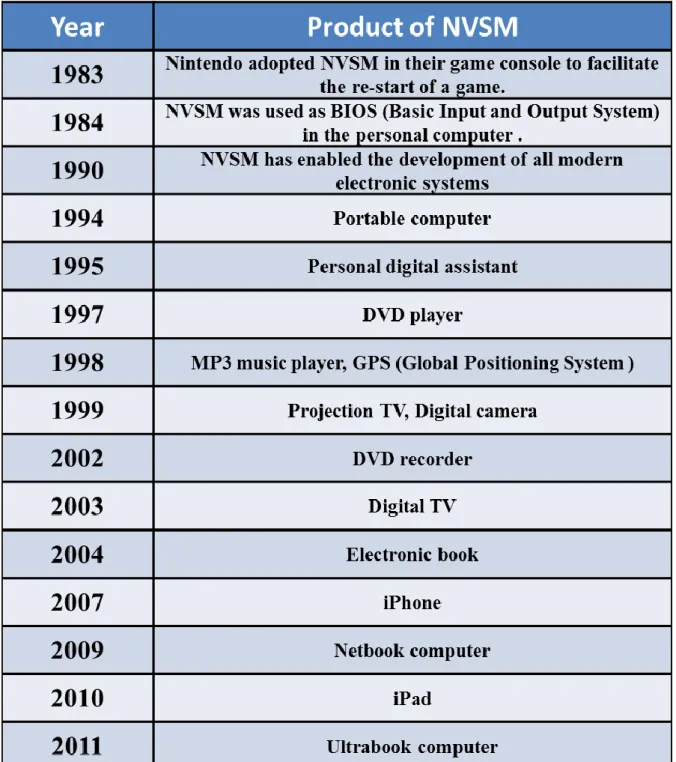
11.1 Overview of Memory Device and its Challenges……….. 1
1.1.1 The Invention of NVSM………. 1
1.1.2 The Developing of NVSM market……… 1
1.1.3 The Scaling Down Challenge of NVSM……...……….. 2
1.2 Alternative Structure of Floating-Gate NVSM……… 3
1.2.1 MNOS and SNOS Devise………...………... 4
1.2.2 SONOS Devise……… 4
1.2.3 Nano-Crystal Device……...……….. 4
1.2.4 TANOS Device………. 5
1.2.5 BE-SONOS Device………. 5
1.3 Brief Introduction of TFT with SONOS NVSM Device……….. 6
1.4 Motivation……….. 6
1.5 Organization of the Thesis...………. 7
Chapter 2 Device Fabrication and Experimental Setup………….
152.1 Introduction………...……… 15
2.2 Experimental Procedure………... 15
VIII
2.4 Method of device parameter extraction……… 17
2.4.1 Threshold Voltage………... 17
2.4.2 Subthreshold Swing……… 17
2.4.3 Transconductance……….. 18
2.5 Operation and Characteristic of Memory……… 18
2.5.1 Program Mechanism……….. 19
2.5.2 Erase Mechanism………... 19
2.5.3 Characteristic of Retention……….. 20
2.5.4 Disturb Characteristics………. 21
Chapter 3 Characteristics of TFT Nonvolatile Memory………….
293.1 Introduction………... 29
3.2 Interface Morphology Dependence……….. 29
3.2.1 Atomic Force Microscopy (AFM) Analysis………... 29
3.2.2 Program/Erase Characteristics………... 30
3.2.3 Transistor Performance………. 30
3.2.4 The Comparison of Off-Leakage………. 31
3.3 Channel Thickness Dependence………... 31
3.3.1 X-ray Diffraction (XRD) Analysis………... 31
3.3.2 Program/Erase Characteristics………... 32
3.3.3 Transistor Performance………. 32
3.3.4 The Comparison of Off-Leakage………. 33
3.4 Annealing Temperature Effect……….. 34
3.4.1 Program/Erase Characteristics………... 34
3.4.2 Transistor Performance………. 34
IX
3.5 Summary……… 35
Chapter 4 Reliability of TFT Nonvolatile Memory……….
554.1 Introduction………... 55
4.2 The Comparison of Retention Characteristics………. 55
4.3 The Comparison of Disturbance Characteristics……… 56
4.4 Summary……… 57
Chapter 5 Conclusions and Future Work………
675.1 Conclusions………... 67
5.2 Future Work………... 67
Reference……….
70X
Table Caption
Chapter 1
Table 1.1 The application of NVSM ………... ………….. 8
Table 1.2 The NVSM technology requirements for NAND-type Flash memory in ITRS 2012. ………... 9
Table 1.3 The NVSM technology requirements for NOR-type Flash memory in ITRS 2012.………... ……….. 9
Chapter 3
Table 3.1 Operation principles and bias conditions utilized during the operation of the TFT nonvolatile memory. ……… 37Table 3.2 The splits of fabrication process conditions. ……….. 37
Table 3.3 The electrical parameters of Fig. 3.4..………... 40
Table 3.4 The electrical parameters of Fig. 3.14………. 46
Table 3.5 The electrical parameters of Fig. 3.23
………..
51Chapter 4
Table 4.1 Voltage conditions utilized during the reliability analysis of the TFT nonvolatile memory. ………... 59Chapter 5
Table 5.1 The comparison of different interface morphology devices………... 69Table 5.2 The comparison of different channel thickness devices………. 69
XI
Figure Caption
Chapter 1
Fig 1.1 Cross-section view of the first non-volatile semiconductor memory
with a floating gate in 1967……… 10
Fig. 1.2 Market share of three NVSM products from year 2000to 2011, and projected to 2020……… 10
Fig 1.3 Current-voltage curves of a floating-gate memory device when there is no charge stored in the floating-gate (curve A) and when an negative charge Q is stored in the floating-gate (curve B)……… 11
Fig 1.4 Current-voltage curves of a floating-gate memory device when there is no charge stored in the floating-gate (curve A) and when an negative charge Q is stored in the floating-gate (curve B)………. 11
Fig. 1.5 Design space analysis for floating gate NOR-type Flash. (a) Design space vanishes for 90nm node device. (b) Design space vanishes for 45nm node devise………...……… 12
Fig. 1.6 Silicon-nitride-oxide-silicon (SNOS) …………...……… 13
Fig. 1.7 Silicon-Oxide-Nitride-Oxide-Silicon (SONOS)……… 13
Fig. 1.8 Nanocrystals memory……… 13
Fig. 1.9 TaN gate- Al2O3 blocking-oxide-nitride-tunneling oxide-silicon (TANOS).………... 14
Fig. 1.10 Band-gap engineered SONOS (BE-SONOS)……… 14
Chapter 2
Fig. 2.1 Schematic of the experimental processes for fabricating TFT-nonvolatile memory………...…… 24XII
Fig. 2.3. The schematic of the oxidation and HF wet etching process. (a) The original channel film. (b) After oxidation process. (c) After HF wet etching process………... 25 Fig. 2.4 The experimental setup of each apparatus for pulse generator and I-V
characteristics measurement of memory cell………. 26 Fig. 2.5 The Id-Vg characteristic for programming state “1” and erase state
“0”, showing the ΔVt and memory window ………. 26 Fig. 2.6 The schematic mechanism of the FN tunneling by our programming
condition………. 27
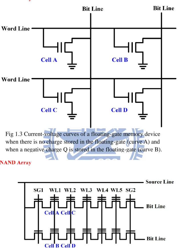
Fig. 2.7 The schematic mechanism of our erasing condition, purple lines are FN hole injection, green lines are band-to-band-hot-hole injection and blue lines are substrate-transient-hot-hole injection……….. 27 Fig. 2.8 The equivalent circuits schematic of the memory cell. During Cell A
is programmed, the gate disturbance takes place in Cell B and the drain disturbance takes place in Cell C……….. 28
Chapter 3
Fig. 3.1 The AFM images of the polysilicon films with oxidation process (a) 0-nm, (b) 10-nm, (c) 20-nm, (d) 40-nm, and removed……….. 38 Fig. 3.2 Program speed characteristic for samples with different
morphologies. ……… 39 Fig. 3.3 Threshold voltage for samples with different oxidation conditions…... 39 Fig. 3.4 Transfer characteristics (Id-Vg curve) with different oxidation
thickness………. 40
Fig. 3.5 Output characteristics (the Id-Vd curve) with different oxidation
XIII
Fig. 3.6 Threshold voltage for samples with different oxidation conditions….. 41 Fig. 3.7 Subthreshold swing for samples with different oxidation conditions… 42 Fig. 3.8 Gm,max for samples with different oxidation conditions………. 42
Fig. 3.9 The gate voltage corresponding to minimum leakage current at fixed drain bias with different oxidation thickness………. 43 Fig. 3.10 The minimum current of the samples with different oxidation
thickness………. 43
Fig. 3.11 X-ray diffraction (XRD) results of polysilicon with different channel thicknesses. (a)50-nm, (b)100-nm, (C)150-nm. These results indicate that thicker poly-silicon have larger grain size……….. 44 Fig. 3.12 Program speed characteristic for samples with different poly-silicon
channel thickness………... 45 Fig. 3.13 Threshold voltage for samples with different poly-silicon channel
thickness………. 45
Fig. 3.14 Transfer characteristics (Id-Vg curve) with different poly-silicon
channel thickness………... 46 Fig. 3.15 Output characteristics (the Id-Vd curve) with different channel
thickness………. 47
Fig. 3.16 Threshold voltage for samples with different channel thicknesses…… 47 Fig. 3.17 Subthreshold swing for samples with different channel thicknesses…. 48 Fig. 3.18 Transconductance for samples with different channel thicknesses…… 48 Fig. 3.19 The gate voltage corresponding to minimum leakage current at fixed
drain bias with different poly-silicon channel thickness……… 49 Fig. 3.20 The minimum current of the samples with different poly-silicon
XIV
Fig. 3.21 Program speed characteristic for samples with for different annealing temperature………... 50 Fig. 3.22 Erase speed characteristic for different annealing temperature………. 50 Fig. 3.23 Transfer characteristics (Id-Vg curve) with different annealing
temperature……… 51
Fig. 3.24 Output characteristics (the Id-Vd curve) with different annealing
temperature……… 52
Fig. 3.25 Threshold voltage for samples with different annealing temperature… 52 Fig. 3.26 Subthreshold swing for samples with different annealing temperature. 53 Fig. 3.27 Transconductance swing for samples with different annealing
temperature……… 53
Fig. 3.28 The gate voltage corresponding to minimum leakage current at fixed drain bias with different annealing temperature………. 54 Fig. 3.29 The minimum current of the samples with different annealing
temperature……… 54
Chapter 4
Fig. 4.1 Retention characteristic for different morphologies at different temperature (a)25oC, (b)75oC, and (c)100oC………. 60
Fig. 4.2 Retention for samples with different channel thicknesses at different temperature 25oC, 75oC, and 100oC………... 61
Fig. 4.3 The schematic of the channel edge damage. (a) The device with channel film 50 nm. (b) The device with channel film 150 nm………. 62 Fig.4.4 Retention for samples with different annealing temperature at
different temperature (a)25oC, (b)75oC, and (c)100oC………... 63
XV
Fig.4.6 Drain disturbance for different interface morphologies. ………... 64
Fig.4.7 Gate disturbance with different channel thicknesses………. 65
Fig.4.8 Drain disturbance with different channel thicknesses……… 65
Fig.4.9 Gate disturbance with different annealing temperature. ………... 66
1
Chapter 1
Introduction
1.1 Overview of memory device and its challenges
1.1.1 The Invention of NVSM
Nonvolatile semiconductor memory (NVSM) was invented by S. M. Sze and Dawon Kahng in April 1967 [1.1]. It is noted that the magnetic core memory (MCM) has many drawbacks, including a large from factor, high power consumption, long access time, and incompatibility with the existing semiconductor technology. In order to alleviate those drawbacks of MCM, S. M. Sze and Dawon Kahng adopted a new structure, a metal layer embedded in the gate oxide of a conventional MOSFET. The structure of first floating-gate nonvolatile memory is shown in Fig. 1.1. There are five layers, including metal (control gate), upper insulator (blocking oxide), metal (floating gate), lower insulator (tunnel oxide) and semiconductor (floating gate) in the floating-gate nonvolatile memory, called MIMIS.
At first, floating gate material adopted zirconium (Zr), because the surface of Zr could be oxidized easily to form ZrO2 as the blocking oxide. However, the lower quality of ZrO2
results the leakage problem [1.2]. To avoid the leakage problem existing in MIMIS structure, floating gate material were replaced by heavy doping Si, called MISIS (metal-insulator-semiconductor-insulator-semiconductor). In this approach, the silicon-dioxide is used as an insulator for its low trap densities, ease of fabrication, and low Si-SiO2 interface states [1.3].
1.1.2 The Developing of NVSM Market
Recently, the applications of the floating-gate memory device have gone far beyond anyone else though it would be. The application of the floating-gate memory is showed in Table 1.1. Undoubtedly, NVSM technology has extensive market requirements, such as
2
computer, personal digital assistant, and electronic portable equipment (USB, MP3 audio player, digital camera, iPod, Ultrabook and so on) [1.4].
Among the current available nonvolatile memory technologies (ROM, EPROM, EEPROM, Flash), Flash memory satisfies many of an ideal memory. There are two major types of Flash memory: one is for code storage applications, and the other is for storage application [1.5]. The structures of NOR and NAND are showed in Fig. 1.2 and 1.3, respectively. NOR-type memory can implement the CHE program, because it has the ground side. Therefore, NOR-type Flash memory has faster program speed than NAND-type. NOR-type memory is suitable for code storage application due to its fast random access speed, such as PC BIOS, cellular phone, application in embedded in system. On the other hand, NAND structure reduces the cell size by connecting the cells in series between a bit line and a source line, leading to eliminate the contact hole [1.6].NAND-type memory has been adopted for data storage, such as Digital Still Camera (DSC), memory care, Silicon Audio and PDA [1.7], due to its high density.Fig. 1.4 shows the market share of the aforementioned NVSM products from the year 2000 to 2011 and projected to 2020 [1.8]. Due to the demand for high-volume storages for portable products, NAND Flash has had the largest market share since 2005.
1.1.3 The Scaling Down Challenge of NVSM
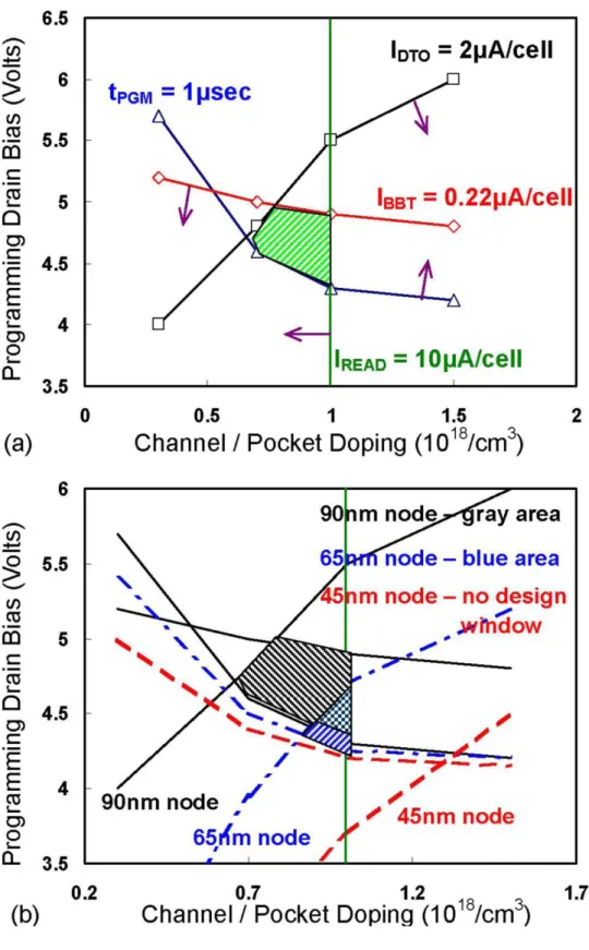
Table 1.2 shows the ITRS roadmap [1.9]. The scaling down would lead to higher density of device, but relentless reduction has created many scaling challenges in last two decade [1.10]. NOR-type Flash memory has two scaling down limits: 1) the non-scalability of the tunneling oxide 2) the challenges of optimizing the junction shape. When the memory is in the retention state, the charges in the floating gate provide a built-in electric field, which makes charges to tunnel out (or for the opposite charge to tunnel in). The previous study had reported that the oxide leakage current at low electric field increases
3
with decreasing the oxide thickness, and this phenomenon is especially serious when oxide thickness beyond 8-nm [1.11]. This is attributed to the defect in the tunneling oxide enhances the probability of charges tunneling back to the channel by Frenkel-Poole mechanism. Therefore, the tunneling oxide thickness should thicker than 8-nm to prevent charges from tunneling out of floating-gate. Moreover, the programming method of NOR Flash memory is channel hot electron (CHE), produced by the strong lateral electric field at the drain edge. Therefore, NOR Flash memory requires an abrupt drain junction, resulting in the serious short channel effect. Fig 1.5 shows the design space of NOR Flash memory. Because of the unscalablity of the tunneling oxide and abrupt junction, the design space would vanish at 45-nm technology node [1.12].
On the other hand, NAND Flash memory operation principle different from NOR Flash, resulting in different scaling limit. NAND Flash uses the Fowler-Nordheim (FN) tunneling mechanism to program, so it does not require abrupt deep junctions. In addition, NAND Flash has larger design space, because of the lower performance requirement compared to NOR Flash. However, NAND Flash faces the intensive challenge, such as floating gate interference, a lower coupling ratio and less tolerant charge loss [1.13]. When the space between word-lines drops below 30-nm, the interference originating from neighboring floating gate for select device will become more serious and the smaller space between word-lines greatly reduced coupling ratio [1.14].
1.2 Alternative Structure of Floating-Gate NVSM
To overcome the scaling limits and enhance the retention of the conventional FG structure, many alternative structures were be proposed, including replacing trapping layer material, improving the tunneling oxide, and adopting high-K metal gate for blocking oxide and control gate. In this section, we would list some common structures.
4
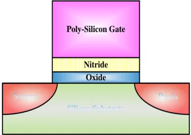
1.2.1 MNOS and SNOS Devise
Metal-nitride-oxide-silicon (MNOS) device, the first electrically alterable semiconductor (EAROM) devices, was invented in 1967 [1.15]. Charges are injected from the channel by quantum mechanical tunneling through the tunneling oxide. In 1980, an important breakthrough was achieved, that transform the metal gate by heavy doping Si-gate SNOS (silicon-nitride-oxide-semiconductor) [1.16]. The cross-section of SNOS is showed in Fig. 1.6. Si-gate fabrication markedly improves the data retention by introducing high temperature H2 annealing, which enhances the interface quality of
nitride-oxide and oxide-Si [1.17].
1.2.2 SONOS Devise
In order to reduce the charges injection from the gate, oxide were provide on top of the nitride, called SONOS (silicon-oxide-nitride-oxide-semiconductor) device [1.18], as illustrated in Fig. 1.7. The benefit of nitride trapping device is that charges are stored in the discrete trapped states. Because charges would not all leaked by local oxide defects generated after program stress, therefore, the tunneling oxide thickness scaling limit of SONOS-type memory can be thinner than FG-type memory [1.12]. In addition, the discrete trapped states make the multi-level-cell (MLC) become possible. On the other hand, nitride is the insulator without floating gate interference.
Besides memory characteristics, SONOS-type memory offers other superiorities compared to FG-type memory: 1) simple fabrication process 2) compatible to CMOS technologies 3) elimination of the drain induced turn on effect [1.19]-[1.23]. For these reasons, SONOS-type memory has great potential to replace FG-type memory.
1.2.3 Nano-crystal Device
5
by Tiwari et al in 1995 [1.24]. The nanocrystals (NCs) memory can be created by break up the floating gate into many nanocrystals poly-silicon dots in a floating gate device [1.25]. Recently, the Si, Ge, high-k dielectric, metal and silicide are used for storage node application in the NCs memory device [1.25]-[1.29]. Like SONOS, NCs memories have discrete trapped states that result faster programming- and erasing – speed than FG- memory. On the other hand, NCs memories have better retention than SONOS-type memory by the deep trap level state of nanocrystals dots.
However, NCs memory will reach the limiting by the amount controlling of NCs. The smaller device dimension, the less amount of NCs. The variation of NCs will become obvious, leading unacceptable variation of threshold voltage in program state.
1.2.4 TANOS Device
Samsung proposed a new structure that replaces blocking-oxide and poly-silicon gate by Al2O3 and TaN gate, respectively in 2003 [1.30]. The structure of TANOS (TaN gate-
Al2O3 blocking-oxide-nitride-tunneling oxide) is showed in Fig. 1.9. The TaN gate has higher work function than the poly-Si gate and Al2O3 has higher dielectric constant than
SiO2. Therefore, it significantly inhibited gate injection effect during FN-erase operation. As the result, both programming- and erasing – speed are improved in TANOS device.
1.2.5 BE-SONOS Device
Macronix proposed the bandgap engineered SONOS (BE-SONOS) memory, replacing the tunneling-oxide by ultra-thin O1/N1/O2 layer as a non-traping tunneling dielectrics showed in Fig. 1.10. Under retention state, charges are blocked by the total thickness on the O1/N1/O2 layer, and the top layer (O2) becomes invisible to the substrate holes in the erase state. Therefore, BE-SONOS offers fast hole erase, and great better retention for the conventional SONOS [1.31].
6
1.3 Brief Introduction of TFT with SONOS NVSM Device
Nearly a decade, low-temperature polycrystalline silicon (LTPS) thin film transistor (TFT) has becomes an appealing research area for their use in active-matrix liquid crystal displays (AMLCDs) [1.32]. Because higher mobility and more stable threshold voltage than a-Si:H TFTs, LTPS TFTs enable the integration of driver electronics, sensors, memories, and peripheral circuits on the glass substrate to produce system-on-panel (SOP) display. Therefore, manufacture the high quality NVSM is an important issue for the realization of SOP.
In LTPS-TFTs, due to the poor thermal conductivity of the glass substrate, manufacturing the high quality tunneling oxide and the optimized retention of TFT-floating gate memory would become difficult. As the result, SONOS-type memory has higher potential for SOP due to its discrete storage node and simple fabrication. How to further enhance TFT-SONOS memory programming/erasing efficiency and improve retention are the important issue.
1.4 Motivation
To realize system-on-plane (SOP) display, the task is to further improve LTPS-SONOS. Such as section 1.2 described, there are some literature proposing that replacing nitride by NCs or high-k material [1.33], optimizing blocking oxide and poly-gate by high-k metal gate [1.34], and improving tunneling oxide by bandgap engineered mechanism [1.31]. However, the impacts of the poly Si channel condition on NVSM are missing.
Apparently, enhancing the local electric field is a direct way to improve P/E speed. The previous study had reported that a Fowler-Nordheim tunnel current is enhanced with the rougher surface [1.34]-[1.35]. Therefore, we want to demonstrate the rougher
7
morphology for faster P/E speed of TFT-SONOS. On the other hand, it is noted that the performance would be altered by different crystallization condition. However, the relation between TFT-memory characteristics and crystallization conditions is still not clear. In this work, the impacts of morphology, channel thickness, and crystallization temperature on the poly-Si TFTs and non-volatile memory would be systematically studied.
1.5 Organization of the thesis
In thr Chapter 1, an introduction about the general background and the scaling challenge of nonvolatile memory devices are described. Moreover, we also introduce the alternative structures (ex. SNOS, SONOS, Nano-crystal memory, TANOS and BE-SONOS) for the purpose of the scaling limits and of the conventional FG. At last, we introduce the motivation of our study.
In the Chapter 2, we report the process of TFT-NVSM with different morphology, channel thickness, and crystal condition. In addition, the measurement condition (such as programming, erasing, retention and disturbance) and the parameter definitions are also presented in this chapter.
In the Chapter 3, the detail study about the TFT-SONOS devices with different morphology, channel thickness, and crystal condition. First, we discuss the P/E efficiency, second the Transistor Performance (Id-Vg, Id-Vd, threshold voltage, transconductance and
subthreshold swing), at last we analyze the leakage current.
In the Chapter 4, we study the reliability issues such as retention, gate disturbance and drain disturbance with different morphology, channel thickness, and crystal condition.
Finally, in the Chapter 5, conclusions of this dissertation and recommendation for further research are presented.
8
9
Table 1.2 The NVSM technology requirements for NAND-type Flash
memory in ITRS 2011 [1.9]
Table 1.3 The NVSM technology requirements for NOR-type Flash
memory in ITRS 2011 [1.9]
10
Fig 1.1 Cross-section view of the first non-volatile
semiconductor memory with a floating gate in 1967.
Metal Gate
Insulator
Insulator
Silicon Substrate
e -e -e- e- e -e-Floating
Gate
Source
Drain
Fig. 1.2 Market share of three NVSM products from year
2000 to 2011, and projected to 2020 [1.8].
11
Fig 1.3 Current-voltage curves of a floating-gate memory device
when there is no charge stored in the floating-gate (curve A) and
when a negative charge Q is stored in the floating-gate (curve B).
Fig 1.4 Current-voltage curves of a floating-gate memory device
when there is no charge stored in the floating-gate (curve A) and
when a negative charge Q is stored in the floating-gate (curve B).
12
Fig. 1.5 Design space analysis for floating gate NOR-type Flash.
(a) Design space vanishes for 90nm node device. (b) Design space
vanishes for 45nm node devise. [1.4]
13
Fig. 1.6 Silicon-nitride-oxide-silicon (SNOS).
Poly-Silicon Gate
Nitride Oxide
Silicon Substrate
Source Drain
Fig. 1.7 Silicon-Oxide-Nitride-Oxide-Silicon (SONOS).
Fig. 1.8 Nanocrystals memory
Oxide Poly-Silicon Gate Oxide Silicon Substrate Source Drain Nanocrystals Oxide Poly-Silicon Gate Nitride Oxide Silicon Substrate Source Drain
14
Fig. 1.10 Band-gap engineered SONOS (BE-SONOS)
TaN Gate Nitride Oxide Silicon Substrate Source Drain Al2O3
Fig. 1.9 TaN gate- Al
2O
3blocking-oxide-nitride-tunneling
oxide-silicon (TANOS)
Oxide
O O NPoly-Silicon Gate
Nitride
Silicon Substrate
Source
Drain
Ultra-thin
ONO
15
Chapter 2
Device Fabrication and Experimental Setup
2.1 Introduction
In the previous chapter, we presented the invention of nonvolatile memory and alternative structures of FG memory. In order to realize the system-on- panel (SOP) and system-on-chip (SOC), integrating NVSM into the thin film transistor (TFT) digital circular is necessary. Unlike single crystal NVSM, TFT device has the poly-Si channel and rougher interface morphology, but it had been not completely studied in literature. In this chapter, we report the process of TFT with different morphology, channel thickness, and crystal condition. Moreover, the measurement condition such as programming, erasing, retention and disturbance are also presented in this chapter.
2.2 Experimental Procedure
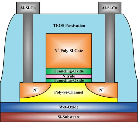
Fig. 2.1 shows the fabrication process of the devices for this work. A 6-in (100) silicon wafer was adopted as the base substrate. First, the 500-nm thermal oxide was grown on silicon wafer by standard furnace. The a-Si layer was deposited by low-pressure chemical vapor deposition (LPCVD) with the thickness 50, 100, 150-nm (Fig. 2.1-(a)), and then wafers were annealed for 24 hour at 580, 600 and 620 °C(Fig. 2.1-(b)). Some samples were grown dry-oxide 10, 20 and 40-nm, and removed it by HF solution. After defining the active regions (Fig. 2.1-(c)), the ONO tri-layer were formed by LPCVD with the tunneling oxide 13-nm, nitride 14-nm and blocking oxide 24-nm. Next, 150-nm n+ polysilicon as the gate electrode was deposited and implanted with phosphorous (40keV at 5×1015 cm-2) (Fig.
2.1-(d)). After gate electrode patterning (Fig. 2.1-(e)), source/drain were implanted with phosphorous (20keV at 5×1015 cm-2) by self-aligned method and activated at 600 °C for
16
24-hr annealing in an N2 ambiance (Fig. 2.1-(f)). The 500-nm TEOS oxide as the passivation layer was deposited (Fig. 2.1-(g)), and the contact hole was patterned. Finally, the 600-nm Al-Si-Cu pad was deposited and patterned to finish the process of TFT-SONOS fabrication. The TFT-SONOS memory structure cross section is illustrated in Fig. 2.1-(h). All process splits are showed in the Fig. 2.2.
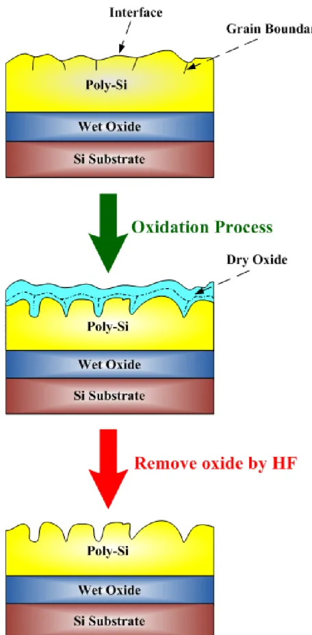
Furthermore, in order to discuss the memory characteristic with different morphology, the different thickness dry oxide were grown and removed by HF. Because of the material characteristics, dry oxide would be grown along grain boundaries. As a result, we could get different morphology by growing different thickness dry oxide and removing it. The process is illustrated in Fig. 2.3.
2.3 Measurement and Equipment Setup
The measurement setup of this TFT-SONOS device is illustrated in Fig. 2.4, including the electrical characterization system characterization system (KEITHLEY 4200), two channel pulse generator (Agilent 81110A), low leakage current switch mainframe (KEITHLEY 708A) and the probe station.
KEITHLEY 4200 equipped with programmable source-monitor units (SMU) and provides a high current resolution to pico-ampere range to facilitate the current measurement. Agilent 81110A with two pulse channels provides the high timing resolution pulse for the P/E characterization of nonvolatile memory. KEITHLEY 708A configured a 10-input×12-outpute switching matrix, that can switches the signals from the KEITHLEY 4200 and Agilent 81110A when the devise is measured in probe station. Moreover, the C++
17
2.4 Method of Device Parameter Extraction
In this section, the definition of electrical parameters are introduced, including the threshold voltage (Vth), subthreshold swing (S.S), and maximum transconductance
(Gm,max).
2.4.1 Threshold Voltage
In this thesis, by fixing drain current method Id=Idn×(W/L) where Idn is a normalized
drain current, the threshold voltage (Vth) is defined as Vg when Idn=10nA. This definition can avoid the ambiguity associated with devices where the effective mobility depends strongly on the gate bias, based on the surface bend bending on the identical gate bias of all devices are the same.
2.4.2 Subthreshold Swing
Depending on the gate and source-drain voltages, the MOSFET Id-Vg curve can be identified as three regions, including the sub-threshold region, saturation region and linear region. In the sub-threshold region, the most important parameter is sub-threshold swing, because it describes how a MOSFET device switches off.
The sub-threshold swing (S.S.) is defined as the reciprocal of slope of the logarithmic scale Id-Vg curve in the sub-threshold region and as the amount of gate voltage required to
upgrade drain current by one order of magnitude. The previous study had reported that S.S. is closely related to the trap states located near the mid-gap (deep states), which originate from dangling bonds and the mobility is associated with the trap states near the band edge (tail state) [2.1-2.2]. Therefore, the S.S and mobility properties are effective to determine the deep state density and tail state density, respectively.
18
2.4.3 Transconductance
Transconductance (Gm) is the guide to obtain the field effect mobility. There are three
stages for Gm-Vg curve (Vd=constant). First stage is drain current in the saturation region (Vg>Vt and Vd>Vd,sat=Vg-Vt), which is proportional to quadratic of Vg-Vt as the eq. 2-1, so
Gm is proportional to Vg-Vt as the eq. 2-2. Id,sat = WL μFECox(Vg−Vt) 2 2 ……….……….……..…(eq. 2-1) Gm≡ ∂V∂Id g = W LμFECox(Vg− Vt) …….…….………..…(eq. 2-2) The second stage is the linear region (Vd<Vd,sat=Vg-Vt), and the drain current is
proportional to Vg-Vt as the eq. 2-3 and Gm is constant as the eq. 2-4.
Id,sat = WL μFECox(Vg− Vt−V2d)Vd ……….………..…(eq. 2-3) Gm≡ ∂V∂Id
g =
W
LμFECoxVd ……….………...(eq. 2-4) When entering the third region, the increase of Vg forces carriers to approach to the
interface, so that the mobility would degradation by surface roughness scattering. As this result, Gm has the maximum at the transition between linear region and saturation region
(Vd=Vd,sat=Vg-Vt) as shown in eq. 2-5. Gm,max ≡∂V∂Id
g =
W
LμFECoxVd ………...………..(eq. 2-5) In this work, KEITHLEY 4200 is adopted to extract gm. By finding out the Gm,max,
we can compare the field effect mobility of all samples as eq. 2-5.
2.5 Operation and Characteristic of Memory
Generally, non-volatile memory device interprets the programmed state “1” and the erase state “0” by threshold voltage. Data was stored successfully by trapping charges in the floating gate, and the definition of memory window is the change of threshold voltage between the programmed state and erased state as show in Fig. 2.5. This section we will
19
introduce P/E mechanism and characteristics of retention.
2.5.1 Program Mechanism
There are wide varieties of program principles of NVM. Fowler-Nordheim (FN) injection [2.3]-[2.5] and channel-hot electron (CHE) injection [2.6]-[2.8] are prevailing in modern nonvolatile industry. For FN tunneling programming, the positive bias is applied to the gate terminal during the programming and the voltage drop across the tunneling oxide make the electric field more than 6MV/cm. The electrons would be injected from channel into trapping layer. The main drawback of FN tunneling mechanism is slower programming speed, compared to CHE, due to lower tunneling current [2.9].
On the other hand, for the CHE, the carriers are accelerated by the horizontal electric field in the channel and obtain high energy in the program process. Therefore, impact ionization would generate electron-hole pairs near drain side, and then the high energy hot electron could be injected into trapping layer by the vertical electric field. Compare to the FN mechanism, CHE has faster program speed and smaller program voltage, but CHE injection causes the tunneling oxide damage near the drain side.
In this thesis, we adopted the FN injection to program. Because the voltage of channel are identical in the inversion mode, the programming condition (Vg=20 V, Vs=Vd=-15V) is
identical to Vg = 35 V as shown in the Fig. 2.6.
2.5.2 Erase Mechanism
SONOS-type NVM device has two common kinds erasing mechanism: Fowler-Nordheim (FN) tunneling and band to band hot holes (BTBHH) injection. For FN tunneling erasing, the negative bias is applied to the control gate and the electron would detrap from the trapping layer. Like programming, the drawback of FN tunneling erasing is the slower erase speed [2.9].
20
There is another common erasing method, Band-to-Band tunneling Hot-Hole (BTBTHH). The negative bias and positive bias are applied to control gate terminal and drain terminal during the erasing, respectively. When the negative gate bias is large enough, the band banding of the drain would become sufficient to generate electrons and holes. Then, the generated holes gain enough energy due to high electrical field and would inject to the trapping layer. BTBHH erasing mechanism has faster erase speed than FN erasing mechanism, but the high energy hot holes injection would cause tunneling oxide reliability issues.
There is another prevailing erasing method, called substrate transient Hot-Hole (STHH) injection. The STHH injection mechanism makes electron/hole pair by changing the junction bias of source/drain-substrate into reverse bias instantaneously. When the junction of S/D and substrate are switch to the reverse bias, a fast discharge and hot carriers are generated by the transient avalanche junction breakdown. Afterward, the hot holes would be extracted with negative gate bias and injection into trapping layer [2.10].
To obtain more uniform holes injection and high erasing speed and avoid gate injection, we adopt the erasing condition (Vg=-9V, Vs=Vd=15V) as shown in Fig.2.7. There
are three mechanisms FN, BTBHH and STHH used in our erase condition. First, smaller negative bias can avoid gate injection but degrade FN efficiency. As a result, we apply the positive bias to the source/drain terminal, BTBHH injection would help to erase efficient. Moreover, STHH injection occurs significantly as source/drain bias be applied.
2.5.3 Characteristic of Retention
For SONOS-type NVM, data retention is an important reliability issue. The previous study had reported that retention capability of SONOS memories has to be checked by using accelerated test such that high electric fields or high temperature [2.11]. In this work, we discuss data retention characteristic after programming with three different
21
temperatures, 25 °C, 75 °C and 125 °C. By way of measure the Vt variation, we can find out the amount of the excess trapping electrons.
2.5.4 Disturb Characteristics
Fig. 2.11 schematically shows the array of NAND architecture. In order to execute programming and erasing with our condition, the common source lines are adopted into this NAND architecture, and the common source voltage is called Vcs. It is known from the literature that the disturbance problems including program disturbance, erase disturbance and read disturbance [2.12][2.13]. The disturbed phenomenon of programming happened to the common word-line device called gate disturbance makes the electrons tunneling into the trapping layer and causes threshold voltage fluctuation. Another gate disturbance situation is that the trapped electrons tunnel from the trapping layer to the control gate via the defects located in the blocking oxide, while the applying voltage of gate terminal is large.
On the other hand, the read disturbance happened to the common bit-line device is called drain disturbance. The drain bias may force electrons to inject into the trapping layer, resulting in unacceptable threshold voltage increase.
In this thesis, the disturbance problems are shown in Fig 2.8. In cell B, high gate voltage stress is generated by the common word-line during the programming of cell A (VWLn =Vg =20 V and VBLi =Vd =Vcs =Vs = -15 V), resulting in the gate disturbance.
Moreover, the cell C meets the drain disturbance by the common bit-line during the erasing of cell A (VWLn =Vg =-9 V and VBLi=Vd =Vcs =Vs =20 V). Because the reading drain bias
(Vd=0.1) is far less than erasing drain bias, we would not discuss the drain disturbance during the reading state.
22 Si-Substrate Wet-Oxide a-Si Si-Substrate Wet-Oxide Poly-Si Si-Substrate Wet-Oxide Poly-Si
(a) Thermal oxide was grown on silicon wafer and the
a-Si layer was deposited by low-pressure chemical
vapor deposition (LPCVD) with thickness 50, 100,
150-nm.
(b) SPC annealed for 24 hour at 580, 600 and 620
°C.
(c) Defining the active regions.
(d) The ONO tri-layer were formed by LPCVD and
150-nm n+ polysilicon as the gate electrode was
deposited and implanted with phosphorous (40keV
at 5×10
15cm
-2).
Si-Substrate Wet-Oxide Poly-Si-Channel Nitride Tunneling-Oxide Blocking-Oxide N--Poly-Si-Gate23
(f) Source/drain were implanted with phosphorous.
(e) Gate electrode patterning.
24
Fig. 2.1 Schematic of the experimental processes for fabricating
TFT-nonvolatile memory.
Fig. 2.2. Schematic of the fabrication process.
Thermally oxidized wafer A,B,C,D,E,F,G,H a-Si 50nm G a-Si 100nm H a-Si 150nm A,B,C,D,E,F 600 oC 24hr Crystallization A,B,C,D,G,H 580 oC 24hr Crystallization E 620 oC 24hr Crystallization F Dry-oxide 10nm B Dry-oxide 20nm C Dry-oxide 40nm D Dry-oxide 0nm A,E,F,G,H
25
Fig. 2.3. The schematic of the oxidation and HF wet etching
process. (a) The original channel film. (b) After oxidation
process. (c) After HF wet etching process.
26
Fig. 2.5 Current-voltage curves of a NVSM device, when there is no
charge stored in the floating-gate (curve A) and when the negative
charges are stored in the floating-gate (curve B).
Fig. 2.4 The experimental setup of each apparatus for pulse generator
and I-V characteristics measurement of memory cell.
27 Si-Substrate Wet-Oxide Poly-Si-Channel Blocking-Oxide
Gate
Drain Sorce Tunneling-Oxide Nitridee
-e
-e
-e
-e
-e
-e
-Vg(+20)
V
d(-15)
V
s(-15)
Fig. 2.7 The schematic mechanism of our erasing condition, purple lines
are FN hole injection, green lines are band-to-band-hot-hole injection and
blue lines are substrate-transient-hot-hole injection.
Fig. 2.6 The schematic mechanism of FN tunneling by our programming
condition.
28
Fig. 2.8 The equivalent circuits schematic of the memory cell. During Cell
A is programmed, the gate disturbance takes place in Cell B and the drain
disturbance takes place in Cell C.
29
Chapter 3
Characteristics of TFT Nonvolatile Memory
3.1 Introduction
The significant demands of nonvolatile memory device are the programming/erasing efficiency and data retention. However, the studies of poly-TFT nonvolatile memory with different channel condition are investigated rarely. In this chapter, the P/E efficiency and electrical characteristics of poly-TFT with different channel condition were studied. First, we discuss the effect of interface morphology by oxidation process. Second, the poly-silicon channel thickness dependence would be reviewed, too. At last, the effect of annealing temperature would be discussed. The P/E conditions are showed in Table 1 and all splits of fabrication processes are showed in Table 2.
3.2 Interface Morphology Dependence
3.2.1 Atomic Force Microscopy (AFM) Analysis
In order to investigate the relation between interface morphology and P/E efficiency, dry-oxide (10, 20 and 40-nm) were grown and removed by HF. The morphology of poly-Si channel after removing dry-oxide is shown in Fig. 3.1. Root-Mean-Square (Rms) of samples is 0.375-nm, 0.788-nm, 1.013-nm and 1.647-nm, respectively. Obviously, the thicker the dry oxide grown on poly-Si initially, the rougher the morphology becomes. This is due to thermal oxide would grow along the grain boundary, leading to the rougher morphology after removing the dry-oxide. As a result, different oxidation conditions can effectively alter the poly-Si channel property.
30
3.2.2 Program/Erase Characteristics
Fig. 3.2 show the memory programming speed at Width/ Length = 10μm/ 10μm, and the programming voltage were at Vg =20 V and Vs= Vd= -15 V. As it expected, rougher
morphology enhances the memory program speed. This is attributed to that the rougher morphology leads to a smaller conduction area and higher localized electric field, subsequently causing a higher electron trapping rate [3.1]-[3.2].
Fig. 3.3 show the memory programming speed at Width/ Length = 10μm/ 10μm, and the programming voltage were at Vg = -9 V and Vs= Vd= 20 V. Unlike programming, the trend for the erase state was not observed. This is attributed to the different barrier height and effective mass of the electron and hole are responsible for the different trend of P/E speed induced by morphology.
3.2.3 Transistor Performance
Fig. 3.4 shows the Id-Vg and Gm-Vg characteristics with different oxidation thickness and the electrical parameters are showed in Table 3.3. Fig. 3.5 shows the drain current– drain voltage (Id-Vd) characteristics with different oxidation thickness for different Vg overdrive voltage (0, 3, 6 and 9 V). These results indicate that sample B has the smallest threshold voltage, steepest subthreshold swing and highest on-state current. In addition, the electrical analyses such as Vth, subthreshold swing, and maximum Gm were performed and
shown in Fig. 3.6, 3.7 and 3.8, respectively.
Sample B exhibits the better performance (S.S., Vth and Gm,max) than the control
sample due to the additional oxidation step which causes the secondary grain growth [3.3]-[3.4], that reduces both interface and intra-grain defects. However, as the oxidation time is increased for sample B and C, the roughness scattering would counteract the secondary grain growth and degrades the mobility. Moreover, the rougher morphology
31
causes more interface defects, so that the subthreshold swing became poorer. These results were similar to previous reports [3.5]. On the other hand, it is observed that sample A and B have more obvious kink current than sample C and D in Fig.3.5. This observation can be possibly ascribed to that the thicker oxidation sample has the thinner poly-silicon channel. Thus, the thinner poly-Si channel exhibits relatively fully deplete at saturation operation, leading to suppress kink effect [3.6].
3.2.4 The Comparison of Off-Leakage
We investigated the relation between minimum current and drain bias in Fig. 3.9 and Fig. 3.10. In this work, Vg,min represents the gate voltage that causes the minimum drain
current (Id,min). The strong observed dependence of the leakage on Vg,min and Vd implies that trap assisted GIDL dominates the leakage current.
Fig. 3.9 shows sample A has higher Vg,min, meaning it’s more easy to generate GIDL current at the low voltage drop Vdg. Moreover, we also observed that Id,min would become
lower by enhancing the oxidation thickness in Fig. 3.10. This observation can be possibly ascribed to that oxidation samples (sample B, C and D) have the extra secondary grain growth step, reducing the inter grain defect as well as trap assisted GIDL effect. Therefore, sample D has the lowest Id,min and Vg,min.
3.3 Channel Thickness Dependence
3.3.1 X-ray Diffraction (XRD) Analysis
Fig. 3.11 shows the X-ray diffraction (XRD) results of poly-silicon channel with different channel thicknesses (50, 100 and 150 nm)
.
As the results, poly-Si grain size would be enhanced by using thicker a-Si channel based on the same thermal budget. This is attributed to that thicker a-Si channel has larger space for grain growth.32
3.3.2 Program/Erase Characteristics
Fig. 3.12 and 3.13 show the P/E speed with different poly-silicon channel thickness. It was showed that no significant difference in the program state; However, the sample- G with the thinnest poly-Si thickness has the slowest erase speed.
This observation can be possibly ascribed to the different mechanisms of programming and erasing. For the programming state, the programming condition as FN-programming (Vg=20 V, Vs=Vd=-15V), is only dependent on the intensity of vertical electrical. Thus, we believe that although thicker poly-silicon channel devices with larger grain size can exhibit the higher horizontal electrical field, but no significant different vertical electrical fields at the interface based on the result. Therefore, there are no significant differences for the programming speed.
On the other hand, there are three different mechanisms of our erasing condition (Vg=-9V, Vs=Vd=15V), including FN, BTBHH and STHH, are shown in Section 2.5.2. FN-erasing efficiency depends on the vertical electrical field, BTBHH-erasing efficiency is dominate by the voltage-drop between gate and drain terminal, and STHH-erasing efficiency is dependent on the junction bias between the source/drain and substrate. Using the same doping and S/D annealing condition, thicker channels would have deeper junction depth, resulting higher quantity of electron-hole pair generation of the substrate transient effect. Therefore, thicker channel devices have higher erasing speed by STHH mechanism. However, the erasing speed have no significant differences between sample H and A, meaning that these samples exhibit the comparable junction depth. In other words, the effective junction depth may be saturated, as the channel thickness we adopted beyond a critical thickness.
3.3.3 Transistor Performance
33
and the electrical parameters are showed in Table 3.4. Fig. 3.15 shows the drain current– drain voltage (Id-Vd) characteristics for different Vg overdrive voltage (0, 3, 6 and 9 V).
Obviously, sample A has the best drain current in saturation range and the largest maximum transconductance.
Fig. 3.16, 3.17 and 3.18 show the electrical characteristics for samples with different channel thickness. The thicker the channel film of the device, the higher trans-conductance would be observed (Fig. 3.18). This observation can be possibly ascribed to that thicker polysilicon has larger grain size. It not only reduces grain boundary density but also decreases the grain-barrier height [3.7]. Also, there are two mechanisms that could explain the Vth and subthreshold swing degradation related to sample-H. The first mechanism is
related to the fully depletion below 100-nm [3.8]. The second possible mechanism is related to the larger grain size above 100-nm. On the other hand, thinner channel device (sample G and H) can reduce kink effect current significantly and the results are shown in Fig. 3.15 [3.9].
3.3.4 The Comparison of Off-Leakage
Fig. 3.19 and Fig. 3.20 show the characteristics of minimum current with different channel thickness. The gate voltage corresponding to minimum current at fixed drain bias for sample G is higher than others, meaning that thin channel device possesses smaller grain size and higher inter grain defects.
However, there is another mechanism affecting Id,min. The thicker the channel thickness of device, the deeper junction depth would be obtained by the same junction annealing temperature. Therefore, although thicker channel device has larger grain size that reduce the inter grain defects, but the deeper junction would result higher leakage current.
34
3.4 Annealing Temperature Effect
In this section, we would discuss memory characteristics and electrical performance for different annealing temperature devices.
3.4.1 Program/Erase Characteristics
Fig. 3.21, 22 show P/E-speed characteristics, and no significant divergence were found based on the annealing temperature investigation. This is attributed to that annealing temperature effect affects the grain growth speed as well as the horizontal electrical field but no apparent enhancement related vertical electrical field at interface. Therefore, we can’t observe significant different of P/E speed (program as FN-programming and erase as FN-, BTBHH-, and STHH-erasing).
3.4.2 Transistor Performance
Fig. 3.23 shows the Id-Vg and Gm-Vg characteristics with different SPC temperature
and the electrical parameters are showed in Table 3.5. Fig. 3.24 shows the drain current– drain voltage (Id-Vd) characteristics for different Vg overdrive voltage (0, 3, 6 and 9 V). It’s
not observed significant different in Fig. 3.23, because the splits of annealing temperature are very close. However, in Fig. 3.24, we can observe low annealing temperature device have slightly high drain current in linear range.
As expected, the deposited temperature exhibits an impact on the electrical properties of sample A, E, and F as shown in Fig. 3.25, Fig. 3.26, and Fig. 3.27. The previous study had reported that grain size is influenced by the annealing temperature with the largest grain size obtained at low annealing temperatures [3.10].Solid phase crystallization (SPC) of amorphous silicon involves two distinct processes, namely the nucleation of seeds (formation of clusters crystalline silicon) and their growth to polycrystalline film [3.11].
35
Because that lower annealing temperature of sample E leads to a lower speed of generation of seeds. Therefore, there are less nucleation sites of seeds for sample E during the same annealing time. As a result, lower annealing temperature devise has the largest grain size after 24 hour annealing, and causes a higher trans-conductance, lower Vth, greater
subthreshold swing.
3.4.3 The Comparison of Off-Leakage
Fig. 3.28 and Fig. 3.29 show the characteristics of minimum current. Although the difference is not significant, we can observe that sample E has the lower Vg,min, representing fewer inter grain defects. This is ascribed to that lower temperature annealing devise has larger grain size. Moreover, there are no significant differences for Id,min in Fig. 3.29, because the splits of annealing temperature are very close.
3.5 Summary
In this chapter, morphology and crystallization conditions of thin film transistor nonvolatile memory were studied. Section 3.2, we find that rough morphology improves program speed, but leads to the degradation of electrical performance. Moreover, extra oxidation step causes the reduction of the intra-grain defects due to the secondary grain growth. As the result, oxidation samples improve the Vth and reduce trap assisted GIDL effect.
In the section 3.3, we observed that thicker poly-silicon channel has larger grain size, resulting in the great performance and the reduction of trap assisted GIDL effect. However, thinner channel devise have great swing and low off-state leakage current by shallower junction depth. Besides, there is no significant correlation between channel thickness and memory characteristics.
36
In the section 3.4, we discuss TFT-memory characteristics with different SPC temperature and not find the different of P/E speed. This is attributed to that grain size can’t affect P/E efficiency by vertical electrical field dominate mechanism and the result is consistent with the results of the section 3.3. On the other hand, lower SPC temperature devices have higher performance and reduce trap assisted GIDL effect, because of larger grain size.
37
Table 3.1 Operation principles and bias conditions utilized during the
operation of the TFT nonvolatile memory.
38
Fig. 3.1 The AFM images of the polysilicon films with oxidation
39
10
-710
-610
-510
-410
-310
-210
-110
0-4
-3
-2
-1
0
A (Without Oxidation)
B (Oxidation 10nm)
C (Oxidation 20nm)
D (Oxidation 40nm)
V
th
(V)
Time (sec)
Vg= -9(V),Vs=Vd=20(V)
W/L=10
(
m
)/10(
m)
Fig. 3.2 Program speed characteristic for samples with
different morphologies.
Fig. 3.3 Threshold voltage for samples with different
oxidation conditions.
10
-710
-610
-510
-410
-310
-210
-110
00
2
4
6
8
10
Vg=20(V),Vs=Vd= -15(V)
W/L=10
(
m
)/10(
m)
A (Without Oxidation)
B (Oxidation 10nm)
C (Oxidation 20nm)
D (Oxidation 40nm)
V
th
(V)
Time (sec)
40
![Table 1.2 The NVSM technology requirements for NAND-type Flash memory in ITRS 2011 [1.9]](https://thumb-ap.123doks.com/thumbv2/9libinfo/8717117.200314/26.892.69.835.125.461/table-nvsm-technology-requirements-nand-flash-memory-itrs.webp)
![Fig. 1.2 Market share of three NVSM products from year 2000 to 2011, and projected to 2020 [1.8]](https://thumb-ap.123doks.com/thumbv2/9libinfo/8717117.200314/27.892.143.745.669.1076/fig-market-share-nvsm-products-year-projected.webp)