I
,
an improvement of 13.4dB in receiver sensitivity. A sensitivity
of -36.8dBm was measured for a 1100 sequence, which agrees very well with the predicted sensitivity of -37.6dBm.
1 u
[788131 optical i n p u t power, dBm Fig. 3 10 Gbitls bit error rate curves
(i) with optical preamplifier (ii) without optical preamplifier
The increased penalty (3.0dB) incurred for a 2’
-
1 PRBS as compared to the 1100 result when using an optical pre- amplifier, is believed to be due t o the impact of patterning ofthe optimal threshold setting in the decision circuit.
Conclusions: A high performance lOGhit/s transmission testbed has been developed and a sensitivity of -20.4dBm has been achieved for a 2’
-
1 PRBS. This is the best reported result for a lOGbit/s pin-FET receiver.A high gain (27.2dB), low noise figure (5.6dB) E D F pre- amplifier pumped at 1480nm has been realised. This optical preamplifier has been used t o achieve a sensitivity of -33.8dBm (325 photonsbit) at 10Gbit/s for a 2’ - 1 PRBS, at
a
wavelength of 1548 nm. This is the highest reported sensi- tivity at lOGbit/s for an EDFA pumped at 1480nm. The result for a 1100 sequence is - 3 6 3 dB m (163 photonbit), which agrees very well with predicted performance. This also indicates that there is potential for improvement in per- formance. By reducing patterning, it is expected that a sensi- tivity of-
35 dBm to - 36 dBm could be achieved at 10 Gbit/s using an EDFA pumped at 1480nm. These results illustrate that erbium-doped fibre amplifiers make 10 Ghit/s transmis- sion viable over cost-effective span lengths.Acknowledgments: The authors would like t o thank the Direc-
tors of BNR Europe Limited for permission t o publish this Letter. B. L. PATEL E. M. KIMBER M. G. TAYLOR A. N. ROBINSON I. HARDCASTLE A. HADJIFOTIOU S. J. WILSON R. KEYS J. E. RIGHTON 10th September 1991 BNR Europe Limited
London Road, Harlow, Essex, United Kingdom
References
1 HENMI, N., et al.: ‘Rayleigh scattering influence on performance of a 10Gbit/s optical receiver with an Er doped fibre amplifier’. OFC ’90, THC5, p. 155
2 BLAIR, L. I., and NAKANO, H.: ‘High sensitivity lOGbit/s optical receiver using two cascaded EDFA preamplifiers’, Electron. Lett., 1991,27, pp. 835-836
SAITO, T., et al.: ‘High receiver sensitivity at lOGbit/s using an Er-doped fibre preamplifier pumped with a 0.98pm laser diode’. OFC‘91, PD14, pp. 65-68
4 DESURVIRE, E., and SIMPSON, I. R.: ‘Amplification of spontaneous emission in erbiumdoped single-mode fibres’, J . Lightwave Technol., LT-7, pp. 835-845
3
CRYSTALLINE P M O S INVERTER USING
A M O R P H O U S T H I N F I L M TRANSISTOR AS
ACTIVE LOAD
Indexing terms: Inverters, Semiconductor devices and materials. Transistors
The integration of the amorphous silicon (a-Si : H) thin film transistor on top of a crystalline ptype silicon metal-xide semiconductor (PMOS) transistor to serve as active load has k e n achieved successfully. The vertical integration of crys- talline silicon and amorphous silicon circuits to form the three dimensional structure is a promising technique for future application in high density memory cells and neural network image sensors.
The recent advance in 4Mbit SRAM’-3 relies on the stacking
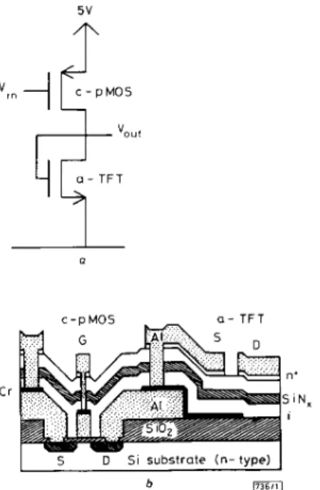
of the load element, i.e. thin film transistor (TFT), on top of the metal-oxide-semiconductor (MOS) transistor. The purpose is to reduce the cell area. We present the results on the successful integration of an amorphous silicon T F T (load) on top of the crystalline p-channel MO S (c-PMOS) transistor. Fig. la and b show the circuit diagram and cross-section of
the integrated crystalline PMOS inverter with amorphous 5 v C
-
PMOS C - D M O S a - T F T SIN,I
s
D S I substrate ( n - t w e )I
bFig. 1 Circuit diagram and cross-section of integrated common gate CMOS circuit consisting of crystalline PMOS and amorphous silicon TFT
a Circuit diagram b Cross-section
silicon T F T (a-TFT) as an active load. The fabrication pro- cesses are as follows. The starting silicon wafer is a lightly doped n-type substrate. After a standard RCA cleaning process, the 7000A field oxide is grown. The first lithographic step is a source and drain patterning, in which the source and drain regions of the MOS field effect transistor are etched using buffered oxide etch. A thin buffer oxide about 300A thick is then grown, followed by source and drain implanta- tion with BF:. The second step is to define the active region. The oxide in this region is first stripped. A 400A thick gate oxide is then regrown, its quality and uniformity being critical in determining the proper device characteristics. The next step is to open source and drain contact regions. The final step is t o pattern A1 followed by annealing a t 350°C for 10min and the crystalline PMOS is completed. The gate length and width
of c-PMOS are 30 and 300pm, respectively.
As for the fabrication processes for the upper a-TFT, the 6rst step is the deposition of 2000A Cr t o serve as etch stop because the etching solution of a-Si : H will also attack the underlying AI.
Afterwards, a n a-Si : H i layer, SiN,, a-Si : H i, and n + layers are grown successively. The first i layer is a buffer layer to separate the gate oxide SiO, and SIN,. It is found that if n o buffer layer is inserted between these two materials, the under- lying c-PMOS will be seriously degraded due to the stress between SiO, and SiN,. SiN, is the gate insulator of the a-TFT, the second a-Si : H i layer serves as the channel and the n + layer is the contact layer. The windows are then opened to contact the underlying Cr. Finally the AI layer is evaporated and patterned and the n + a-Si : H layer is then etched away by reactive ion etching (RIE). This completes the entire fabrication processes. The gate length and width of the a-TFT are 25 and 400ym, respectively.
Fig. 2a shows the common source I-V characteristics of the c-PMOS in this integrated inverter. The gate bias V, varies
In the fabrication of the a-TFT onto the crystalline PMOS, a new technique of inserting an a-Si : H i layer between SiO,
".
0 4 a F O2
I 3"
4 1 n 1 2 3 4 5 age V, V1736131
volt,-I 0 1 Fig. 3 I-V characteristics of a-TFT loud with drain and gate shorted
:j=;l
L L 7:
-0 4 2 -0 2 0 0 - 1 -2 -3 -4 - 5and SiN, layer successfully solves the stress problem and pre- serves the usual performance of the crystalline MOSFET. The success of the integration of crystalline silicon device and amorphous silicon device is a key step in future three dimen- sional memory cell and neural network applications.
drain voltage V&V
(1
0 1 2 3 4 5
I n p u t voltage VI,,. V
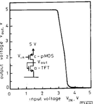
Fig. 4 Transfer curve of integrated circuit using a-TFT as active load
3 0 - 3 - 6
gate v o l t a g e .VG5,V
b
1736121
Fig. 2 Common source I-V characteristics of c-PMOS in this integrated inverter and I-V transfer charucteristics of c-PMOS in integrated circuit
a Common source I-V characteristics Gate bias V, varies from 0 to - 6 V b I-V transfer characteristics
Drain voltage V,, is kept at constant -0.1 V
from 0 to - 6 V . Fig. 26 displays the transfer I, against V,,
curve with drain voltage VDs = -0.1 V. The threshold voltage is 1.5V. The hole mobility as calculated from the trans- conductance is 39 cm2/v s. Fig. 3 shows the I-V characteristics of an a-TFT load with gate and drain shorted. This I-V char- acteristic indicates that the equivalent resistance of the active load is not constant and is large at low gate bias. The drain current has not saturated a t
a
drain bias of 5 V. Fig. 4 shows the transfer curve of this inverter. When the input voltage (gate voltage of c-PMOS) is below 3.2V. the c-PMOS is onwhile the dynamic resistance of the a-TFT is high, which makes the output voltage
V,,,
high; when the input voltage is more than 3.5V, the c-PMOS is turned off and the output voltage is pulled down t o less than 0.5V. In conclusion, the integration of amorphous Si : H T F T on top of crystalline PMOS to serve as active load has been successfully achieved.Acknowledgment: This work is supported by the National Science Council of the Republic of China under contract No. NSC 80-0417-E002-04.
H.-C. LIN 4th September 1991
W.-J. SAH S.-C. LEE
Department of Electrical Engineering National Taiwan University Taipei, Taiwan, Republic of China
References
1 ADAN, A. o., SUZUKI, K., SHIBAYAMA, H., and MIYAKE, R . : 'A half- micron SRAM cell using a double-gated self-aligned polysilicon PMOS thin film transistor load'. Proc. IEEE 1990 Symp. VLSI Technology, 1990, pp. 19-20
UEMOTO, Y., RIIII, E., NAKAMURA, A., and SENDA, K.: 'A high- performance stacked-CMOS SRAM cell by solid phase growth technique'. Proc. IEEE 1990 Symp. on VLSI Technology, 1990, 2
pp. 21-22
KUBOTA, K., MATSUOKA, F., OYAMATSU, H., OCHII, K., and MACGUCHI, K.: 'TFT (thin film transistor) cell technology for 4Mbit and more high density SRAMs'. Proc. IEEE 1990 Symp. on VLSI Tech- nology, 1990, pp. 2 3 2 4
3 KINUGAWA, M., KAKUMA, M., YOSHIDA, T., NAKAYAMA, T., MORITA, S.,
ELECTRONICS LETTERS 7th November 1991 Vol 2 7 No. 23