國 立 交 通 大 學
電子工程學系 電子研究所碩士班
碩 士 論 文
低功率管線式類比數位轉換器的設計與分析
Design and Analysis of Low Power Pipelined
Analog-to-Digital Converter
研 究 生:張仲儀 Johnny Chang
指導教授:羅正忠 博士 Dr.Jen-Chung Lou
低功率管線式類比數位轉換器的設計與分析
Design and Analysis of Low Power Pipelined
Analog-to-Digital Converter
研 究 生:張仲儀 Student : Johnny Chang
指導教授:羅正忠 博士 Advisor : Dr. Jen-Chung Lou
國 立 交 通 大 學
電子工程學系 電子研究所碩士班
碩 士 論 文
A thesis
Submitted to Department of Electronics Engineering & Institute
of Electronic College of Electrical and Computer Engineering
National Chiao Tung University
in Partial Fulfillment of the Requirements
for the Degree of Master
in
Electronic Engineering
January 2008
Hsinchu, Taiwan, Republic of China
低功率管線式類比數位轉換器的設計與分析
研究生:張仲儀 指導教授:羅正忠 博士
國 立 交 通 大 學
電子工程學系 電子研究所碩士班
摘要
近年來,隨著數位電路的發展,系統整合變成主要趨勢,因此電路的面積和其功
率消耗必需愈小愈好。在本論文中將以幾個傳統的低功率設計技巧互相搭配來
完成一個十位元以及四千萬赫茲/秒取樣頻率的管線式類比數位轉換器。
論文中最主要的是以一個預先充電式(雙密勒電容式)的取樣保持電路來降低
第一級放大器設計的難度,而在電源電壓三伏特之下,利用差動的方式將訊號表
式範圍提高到四伏特以便簡化元件匹配及雜訊的問題,並搭配放大器共用的技
巧進而降低功率消耗。本研究使用
TSMC 2P4M 0.35um 的製程去模擬所設計的
電路,根據模擬結果,在電源三伏特下,輸入差動訊號為正負二伏特,取樣頻率為
四千萬赫茲/秒,有效位元達到九點四個位元,整體功率消耗為四十五微瓦特
Design and Analysis of Low Power Pipelined
Analog-to-Digital Converter
Student: Johnny Chang Adviser: Dr. Jen-Chung Lou
Department of Electronics Engineering and Institute of Electronics
National Chiao Tung University, Hsinchu, Taiwan
Abstract
In recent years, digital products play an important role in IC design business. Accompanying with
development of digital circuit system integration becomes a trend, where low power and small area of circuits is the basic requirements. In this thesis we use several old techniques for low power to design a 10-bit, 40M/s sampling rate pipelined analog-to-digital converter.
The primary feature in the thesis is the use of precharged (double miller capacitors) sample-hold amplifier to ease the design of analog amplifier and opamp sharing to further reduce the power dissipation. We also use differential voltage of 4Vp-p to be the reference voltage. The large reference voltage makes noise issues become less important. In this research, pipelined ADC has been designed with standard TSMC 2P4M 0.35um COMS technology. Simulated results show that under 3V supply voltage and input range of 4Vp-p, the designed pipelined ADC can operate at sampling rate of 40MHz, effective numbers of bit of 9.4 bits and total power consumption of 45mW.
致 謝
在交大碩士班這兩年多,隨著這本論文的完成也將結束,而這也可能是我求
學時期的終點,但我知道,學習卻不會因此而間斷,因為接下來的兵役和嶄新的
職場生活將會是我的另一個挑戰。
在這兩年多的期間我要感謝我的父母,他們對我的鼓勵和期望讓我有繼續
努力的動力,每次有空回家時都讓我特別感到家的溫暖。我要感謝指導教授羅
正忠老師在專業上的指導,當然包括那些修課的任課老師也給予我許多電路設
計上的指正。我要感謝林柏村學長和他的學生志瑋帶我度過碩一上這個過度時
期,還有在修課時認識電控所的嘉明,以及我的大學同學志煌總是在 MSN 上給我
鼓勵。我要感謝實驗室裡一起奮鬥的伙伴們,像是建華、修豪等學長讓我在碩
一時有了一盞明燈,以至於不會太迷惘;陪我打撞球的忠樂、愛吃美食的昱鈞、
在唸博班的智仁、愛在實驗室連線的嘉宏等都陪我度過這最困難的碩士班生
活。
要感謝的人太多,最後只好感謝交大提供這麼優美的校園環境和極具優良
的師資,不管在人文和學術風氣上都讓我覺得來到交大真是不虛此行阿!優秀
的交大讓我深深以他為榮,未來期許自己能在事業、家庭、朋友關係中有出色
的表現,讓交大也以我為榮。
張 仲 儀
誌於 風城交大
九十七年 冬
Contents
Abstract (in Chinese)……….Ⅰ
Abstract (in English)……….Ⅱ
Acknowledgement………..Ⅲ
Contents………..Ⅳ
Figure Captions……….Ⅶ
Table Captions………..ⅩⅠ
Chapter 1 Introduction ………...………1
1.1 Background 11.2 Introduction to Low Power Pipelined ADC 1
1.3 Motivations 3
1.4 Organization of the Thesis 4
Chapter 2 Precharged Sample-and-Hold Amplifier………..…7
2.1 Switch Design 7
2.1.1 NMOS Switch 7
2.1.2 CMOS Switch 7
2.2 Introduction to Precharged SHA 8
2.3 Opamp Design 9
2.3.1 DC Gain Requirement 10
2.3.3 Unity-Gain-Frequency Requirement 11
2.4 Bootstrapped Switch Design 11
2.5 Capacitor Size Selection 12
2.6 Simulation Results 13
2.6.1 Opamp Simulated Results 13
2.6.1.1 Input-Referred Offset Voltage Simulation 13
2.6.2 Bootstrapped Switch Simulated Results 14
2.6.3 Precharged SHA Simulated Results 15
2.6.3.1 Ideal-Switch Preaharged SHA Simulated Results 15
2.6.3.2 Bootstrapped-Switch Precharged SHA Simulated Results 15
2.6.4 Final Results and Discussion 16
Chapter 3 Multiplying Digital-to-Analog Converter ………34
3.1 Introduction to Multiplying Digital-to-Analog Converter (MDAC) 34
3.2 Differential Comparator Design 34
3.2.1 Differential Comparing Circuit Design 34
3.2.2 Preamplifier Design 35
3.2.3 Latch Design 36
3.3 Opamp Design 36
3.4 MDAC Design 37
3.5 Simulated Results 38
3.5.1 Differential Comparator Simulated Results 38
3.5.1.1 Input-Referred Offset Voltage Simulation 39
3.5.2 Opamp Simulated Results 39
Chapter 4 Pipelined Analog-to-Digital Converter ………...56
4.1 Clock Generator 56
4.2 ADC Design 56
4.2.1 Analog Path of ADC 56
4.2.2 Digital Path of ADC 57
4.3 Simulated Results 58
4.3.1 Clock Generator Simulated Results 58
4.3.2 ADC Simulated Results 58
Chapter 5 Conclusions and Future Works ………69
5.1 Conclusions and Future Works 69
References ………...70
Figure Captions
Chapter 1
Fig 1.1 Connection between analog world and digital world ………..5
Fig 1.2 Classification of ADC applications according to sampling rate and resolution ………..5
Fig 1.3 10-bit Pipelined ADC structure ………...6
Fig 1.4 Simplified circuit for modeling a typical feedback amplifier ………..…………...6
Chapter 2
Fig 2.1 NMOS switch configuration ………..17Fig 2.2 NMOS channel resistance versus input signal level ………..17
Fig 2.3 CMOS switch configuration ………..18
Fig 2.4 CMOS channel resistance versus input signal level ………..18
Fig 2.5 Precharged SHA configuration ………..19
Fig 2.6 Clock phases used in Precharged SHA ………..19
Fig 2.7 Telescopic opamp with continuous common mode feedback (CMFB) circuit ……….20
Fig 2.8 Precharged SHA in the hold mode and take some parasitic capacitors into account …………20
Fig 2.9 Bootstrapped analog switch configuration ………21
Fig 2.10 Linear phase response of first-order low pass filter ………21
Fig 2.11 Channel resistance of Mc-vgs in bootstrapped analog switch versus input signal level ………22
Fig 2.12 Gain and phase response of telescopic opamp ………22
Fig 2.13 Input/Output transfer curve of telescopic opamp ………23
Fig 2.14 Input common mode range of telescopic opamp ……….23
Fig 2.15 Simulated input-referred offset voltage over 200 Monte Carlo indices ………..24
Fig 2.16 Distribution of input-referred offset voltage ………...24
Fig 2.18 Input and output voltages of bootstrapped analog switch ………...25 Fig 2.19 Phase response of bootstrapped analog switch ………....26 Fig 2.20 Frequency spectrum of bootstrapped analog switch when 2.5V and 20MHz single-ended input voltage is presented ………..………..…………..26 Fig 2.21 Simulated SFDR of bootstrapped analog switch at 2.5V input voltage versus input signal frequency ………...27 Fig 2.22 Simulated SFDR of bootstrapped analog switch at 20MHz input frequency versus input signal level ……….27 Fig 2.23 Precharged SHA with real transistor implementation, where the bootstrapped analog switch configurations are shown in Fig 2.9 ………...28 Fig 2.24 Transient simulation of a precharhed SHA with implementation of real transistors ………...28 Fig 2.25 Frequency spectrum of ideal-switch SHA at frequency of 20MHz and differential input of
4Vp-p ………29
Fig 2.26 Simulated SFDR of ideal-switch SHA versus input signal frequency ………29 Fig 2.27 Simulated SFDR of ideal-switch SHA versus input signal level ………30 Fig 2.28 Frequency spectrum of bootstrapped-switch SHA at frequency of 20MHz and differential input of 4Vp-p ……….30 Fig 2.29 Simulated SFDR of bootstrapped-switch SHA versus input signal level ………31 Fig 2.30 Simulated SFDR of bootstrapped-switch SHA versus input signal frequency ………...31
Chapter 3
Fig 3.1 A radix-2 1.5-bit switch-capacitor pipeline stage schematic ………42 Fig 3.2 Differential comparing circuit ……….42 Fig 3.3 Circuit connection in two phases (a) Sample the reference voltages on capacitors (b) Sample the signal voltages on capacitors ……….43
Fig 3.5 Preamplifier and latch configurations ………..44
Fig 3.6 Two-stage opamp structure with two dynamic common mode feedback (CMFB) circuits…..44
Fig 3.7 Simplicity of a differential ×2 amplifier used for understanding the gain and speed requirements of opamp ………..45
Fig 3.8 Common mode feedback (CMFB) used in two-stage opamp ………...45
Fig 3.9 The MDAC schematic and capacitors values are shown for the first stage of MDAC ……….46
Fig 3.10 Clock phases used in MDAC ………..46
Fig 3.11 Transfer curve of MDAC ………47
Fig 3.12 Simulated transfer curves when reference voltage (Vref) is (a)1V (b)-1V ………..47
Fig 3.13 Digital output of comparator when inputs a certain signal pattern ……….48
Fig 3.14 Statistics of comparator’s output voltage over 600 Monte Carlo indices ………48
Fig 3.15 Gain response and phase response of two-stage opamp ………..49
Fig 3.16 Transconductance of input differential pairs versus input common mode voltage ………….49
Fig 3.17 Transient simulation when unity-gain feedback is connected and inputs a pulse voltage …..50
Fig 3.18 Transient simulation of output common mode voltage ………...50
Fig 3.19 Simulated output offset voltage of two-stage opamp over 200 Monte Carlo indices ……….51
Fig 3.20 Simulated transfer curve of MDAC ………51
Fig 3.21 Block diagram for catching the settled signal of MDAC’s output ………..52
Fig 3.22 Input and output signals of the circuit diagram shown in Fig 3.21 ……….52
Fig 3.23 INL error of MDAC’s transfer function ………..53
Chapter 4
Fig 4.1 State diagram of clock generator ………...61Fig 4.2 Clock generator schematic ………61
Fig 4.3 Positive-trigger D flip-flop ………62 Fig 4.4 Two consecutive stages of MDAC using opamp sharing (a) sample phase in the first stage (b)
amplification phase in the first stage ……….62
Fig 4.5 Analog path of pipelined ADC ………..63
Fig 4.6 Entire ADC architecture ………63
Fig 4.7 Digital error correction structure ………...64
Fig 4.8 Simulated clock phases of synchronous sequential clock generator ……….64
Fig 4.9 Circuit connection for simulating ADC performance ………...65
Fig 4.10 Simulated DAC’s output signal from Fig 4.9 ………..65
Fig 4.11 Simulated DAC’s output spectrum ………..66
Fig 4.12 Histogram of number of hits at each code ………66
Table Captions
Chapter 2
Tab 2.1 RMS noise voltage on a capacitor ………32
Tab 2.2 Transistor sizes of telescopic opamp ………32
Tab 2.3 Telescopic opamp performance summary ……….32
Tab 2.4 Transistor sizes of bootstrapped analog switch ……….33
Tab 2.5 Switch sizes of precharged SHA ………...33
Tab 2.6 Precharged SHA performance summary ………...33
Chapter 3
Tab 3.1 Switch sizes of comparing circuit ……….53Tab 3.2 Transistor sizes of preamplifier and latch ……….53
Tab 3.3 Dynamic comparator performance summary ………54
Tab 3.4 Transistor sizes of two-stage opamp ……….54
Tab 3.5 Switch sizes of common mode feedback used in two-stage opamp ……….54
Tab3.6 Performance of two-stage opamp ………..54
Tab 3.7 Switch sizes of MDAC ……….55
Chapter 4
Tab 4.1 State-assigned table for state diagram in Fig 4.1 ………..67Tab 4.2 Clock generator performance summary ………68
CHAPTER 1
Introduction
1.1 Background
Analog-to-digital converter (ADC) has revolution for years. Now it becomes an indispensable product for many electronic systems. Because the world we live is an analog world, such as lights, heats, forces, waves, etc, all kinds of staffs we’ve seen and heard are analog signals. It is important to convert these analog signals into digital signals for storing and evaluating in digital circuits. In Fig 1.1 we can see the connection between computer and a real world. There are lots of applications in our life and we use them everyday. For example, digital camera, it converts the analog pixel information into digital information and processes them by DSP chips. Also it has wide applications, such as audio systems, video systems, medical instruments, mobile communications, wireline communication, control systems, etc. All kinds of these applications bring us to the world of entertainment. Depending on applications the ADC with different resolution and sampling rate has to be chosen correspondingly. Let us see Fig 1.2 to clearly know the correspondent applications. This figure also points out what kind of ADC architecture should be used for a given resolution and sampling rate. With medium resolution and sampling rate the opamp-based ADC is used often. There is an essential challenge the ADC is facing, power consumption. For many computer systems we might consider to integral all circuit blocks together including digital, analog and mix-signal circuits. Integration means that low power is necessary. For designing a low power ADC there are so many fantastic methods to implement it. In the next section we will talk about some old methods but put them together to really perform a low power pipelined ADC.
Shown in Fig 1.3 is the block diagram of pipelined ADC. The first stage called SHA samples an analog signal and the following ten stages quantify the sampled signal. This pipelined ADC has one analog input and ten parallel outputs. In Fig 1.3 the signal passes to the next stage every one clock cycle. While after ten clock cycles the pipelined stages have been filled up and then the digital outputs will be produced every one clock cycle. One clock cycle generates one 10-bit parallel digital outputs is why the pipelined ADC is often used in high speed applications. In submicron CMOS technology and the rapid revolution of digital circuits, it is necessary to combine analog and digital circuits together for power issues. The other essential issue of analog circuits is the noise. The RMS noise voltage in ADC has to be smaller than 1 LSB of ADC and we know that it must waste power to get low noise. For a given reasonable noise level designing low power ADC is now having a challenging test to take. Especially in opamp-based ADC the noise is an essential issue for ultra low power design. However, the resolution of ADC is mostly determined by CMOS technology and it could achieve 0.1% accuracy of the ratio of two devices if careful layout is effectuated. Some other methods called delta-sigma converters and digital calibration converters are often used to achieve high resolution. Now we continue to introduce and explain some techniques for designing the low power pipelined ADC.
(1) Precharged SHA is used in the first stage [1][2], which has benefit of low power analog opamp. By precharging the output capacitors technically relax the design of opamp, having low power circuit could be achieved.
(2) In 10-bit pipelined ADC shown in Fig 1.3 the gain accuracy, settling speed and offsets requirement become less important when we move down the line [3]. Smaller (and thus low power) stages can be used for later stages having, possibly, a dramatic effect on both layout size and power dissipation.
(3) In Fig 1.3 the amplifier in each stage is used for only half of a clock cycle. Every consecutive stages do not perform amplification at the same clock cycle so significant power reduction can be achieved by sharing an amplifier between every consecutive stages [4][5]. For example, the
first and the second stages of quantization circuit can use only one opamp back and forth when amplification is needed.
(4) In pipelined stages we have options that how many bits each stage can solve. We have solution from predecessors [6] that solving multiple bits in the first stage would save power but consequently slow down the circuit.
(5) Reference voltage is the voltage range used to represent the signals. First thing when designing an ADC is to decide how large your reference voltage is (may also be presented in differential form). As the supply voltage scaling down, the voltage available to represent the signal reduce, therefore, dynamic range becomes an important issue [7]. The dynamic range can be written as:
(
)
2 ddV
DR
KT
C
α
∝
(1.1) , where DR is the dynamic range, K and T are Boltzmann’s constant and absolute temperature respectively and α represents what fraction of the given supply voltage is being utilized. Finally, we can get some insight from Fig 1.4 and use the concluded expression to show the relation between power and other parameters, and which is given by:2 gs t s dd
V
V
P
KT DR
f
V
α
−
⎛
⎞
∝
⋅
⎜
⎟
⋅
⎝
⎠
(1.2) , where P is the power consumption, fs is the given sampling rate and (Vgs-Vt) is the overdrivewhen we model the opamp as a single transistor. In (1.2) we saw that for an given dynamic range, amplifier’s performance and sampling rate the power dissipation is minimized if we increase the fraction of a given supply voltage to represent the signals.
1.3 Motivations
Today is the day called “Digital World”. Digital world makes unportable products become portable, unmemorable become memorable, hard to process become easy to process. However,
digital circuits dominate the electronic technologies while the most important thing is that our world is really an analog world. Analog world must be transferred through the “box” called ADC to becoming a Digital world. This is why an ADC is so necessary and is not going to be endangered. The challenges the ADC encountered need lots of tricks playing around to solve them. That is why so many companies in the world really feel it interesting and they know this will be the exciting thing forever. Having dreams lead people to happiness. There are always some people there insist their dreams and make the world colorful. This is why this work worth to do and the results of these people’s hard working will lead the world to be more colorful.
1.4 Organization of the Thesis
There are five chapters in the thesis. Chapter 1 is the introduction to ADC talking about background and motivations of research in ADC. Chapter 2 is the design and simulation of precharged SHA. The results of each circuit block in SHA will be shown at the end of this chapter. Chapter 3 is the design and simulation of Multiplying Digital-to-Analog Converter (MDAC). In this chapter the process variation in comparator will be simulated. After all the circuit blocks being done we move to Chapter 4, where we will talk about whole ADC architecture using circuit blocks designed before. The effective number of bits (ENOB), INL and DNL will be simulated. Finally, Chapter 5 is the conclusion about this research.
Fig 1.1 Connection between analog world and digital world
Fig 1.3 10-bit pipelined ADC structure
CHAPTER 2
Precharged Sample-and-Hold Amplifier
2.1 Switch Design
2.1.1 NMOS Switch
This section will introduce NMOS and CMOS switches which are used a lot in designing mixed-signal circuits. Shown in Fig 2.1 is a simple NMOS switch controlled by a clock signal. When clock goes low, the charge in the channel will inject to both sides equally, which can be written as:
(
GS- T)
ch ox
Q =C WL V V (2.1) , in which we assume that impedance on the both sides are equal. This charge injection will cause voltage stored on a capacitor change, therefore, destroy the information we want. Also, the channel resistance is written as:
(
)
1 ch n oxW
GS TR
C
V
V
L
μ
−⎡
⎤
=
⎢
−
⎥
⎣
⎦
(2.2) , it is an important design consideration when speed becomes an issue. Shown in Fig 2.2 is channel resistance with different channel widths versus input signal level.2.1.2 CMOS Switch
When large signal has to be process, we might consider using CMOS switch shown in Fig 2.3. In the same design manner, charge injection and channel resistance are important parameter. The charge injection of CMOS switch is difficult to express, but it is often much smaller than that of NMOS switch. In circuit design, the charge injection problem will be conquered by some techniques. The channel resistance of CMOS switch is written as:
( )
(
)
( )
( )
( )
1 { } ch n ox dd tn n ox p ox in n n p p ox tp p W W W R C L V V C L C L V W C L Vμ
μ
μ
μ
− ⎡ ⎤ = − −⎢ − ⎥⋅ ⎣ ⎦ − (2.3), we see that if we can make n oxC (W )n p oxC (W )p
L L
μ =μ , then the channel resistance is independent of input signal level [8]. Fig 2.4 shows the channel resistance with different sizes of NMOS and PMOS versus input signal level. It is apparent to see that large transistor size can have small and constant resistance.
2.2 Introduction to Precharged SHA
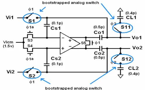
Precharged SHA and also called double miller capacitors SHA is shown in Fig 2.5. It can be seen that in the sample mode signals are sampled on both Cs and CL, which is the loading of the
next stage. Having this design manner the output is precharged to approximate desired voltage in sample mode. When in the hold mode, which forms the miller capacitor around the opamp, the output signal would not vary considerably, so the opamp’s output voltage could stay nearly at the common mode voltage, therefore, low power and small output swing could be achieved. Also, clock phases are shown in Fig 2.6. When ψ1 is high, it is in the sample mode. ψ1ais off before
ψ1 because it would disable the path to be injected charge. This clock phase arrangement is called bottom plate sampling [9]. When the instant of ψ1a goes low, the outputs start to hold the
voltages sampled before (the charge stored on Cs is unchanged). When at the end of ψ2 the hold
signal is stable and then the low of ψ2 is the time when the next stage is processing this
sampled signal. In fact, the exact voltage at the output is not the point, but the charge stored on capacitor is. Ideally the charge stored on Cs does not change either in the sample mode or the hold
mode unless the charge injections are considerable. As we mentioned before the combination of Cs
and Co in the hold mode forms a miller capacitor, reducing the charge injections dramatically from
switches S1 to S4. Since we use differential structure and the information is stored as the type of
So the input common mode voltage of amplifier is defined at the middle of opamp’s input common mode range, while output common mode voltage is defined at the middle of supply voltage.
Now we discuss the noise issue in SHA. The noise in the integrated circuits is expressed as power. In Fig 2.5 both the sample mode and hold mode contribute the noise to the outputs. We first express the output noise power in the sample mode as:
2 . S O L n s
KT
V
C
C
C
=
+
+
(2.4) ,where K is Boltzmann’s constant and T is absolute temperature. Then in the hold mode the outputnoise is described by:
(
)
(
)
(
)
2 . //4
. 1
3
S S L S pi n h e piKT C
C
V
n
C C
⎡ +C C
⎤ ⎣ ⎦+
=
+
(2.5) , where Cpi is the input capacitor of the opamp and ne is the noise contribution factor of the opampdue to the other noise source except the input transistors, and it depends on the architecture of the opamp [1]. These two noise power values should be added to obtain the total noise power.
2.3 Opamp Design
Fig 2.7 shows a telescopic opamp. Telescopic opamp has the advantages of low power, high gain, high speed and low noise, but it suffers from small output swing. Listed above are the properties of telescopic opamp, the real performance is determined by designers in terms of system requirements and the tradeoffs between each of them. Now we talk about some concerns for designing this opamp: (1) slew rate is not we concern since output voltage is much stable and the differential inputs will not drive it out of its linear range. (2) small output swing can be designed, therefore large overdrive of transistors and high speed are achieved. (3) input common mode range need not to be large unless switch charge injections are very large, which is controlled by designing switches to be small. (4) speed and phase margin are much complicated to describe and they depend on how much loading of the next stage is. (5) common mode feedback amplifier
(CMFB) could not tolerate large output swing, so the overdrive of differential pairs in CMFB (Mc1~Mc4) have to be chosen carefully [9]. Now we move to specify the specifications of the
opamp used in precharged SHA mathematically.
2.3.1 DC Gain Requirement
In the feedback amplifier, feedback network is usually formed by passive component such as resistors and capacitors and its gain is determined by its ratio. In this feedback SHA system, the forward path, i.e. opamp, has high gain to perform virtual short at the input differential voltage. If gain is not large enough, the inputs would have a little differential voltage, therefore, causing the feedback amplifier’s gain deflect from its ideal value. Precharged SHA is supposed to have gain of one in the hold mode if opamp’s gain and bandwidth are infinite. First if we consider the DC gain only we could write the input/output transfer function in the hold mode as:
1
1
1
1
.
L1
O O co cl i i iV
C
V
V
V
A V
A C
V
⎡
⎛
⎞
⎛
⎞
⎤
= ⋅ +
⎢
⎜
− +
⎟
⎜
−
⎟
⎥
⎝
⎠
⎝
⎠
⎣
⎦
(2.6) , where Vi is voltage stored on Cs at the end of ψ1a , Vco and Vcl are voltages stored on Coand CLat the end of ψ1, respectively. Now assume that Vco/Vi and Vcl/Viare about 0.96 if input signal is
limited in 20MHz. To achieve 10-bit accuracy, the deviation of Vo from Vi should be less than
1/2N+1 (0.00049) of V
i. With these assumption, substitute them into (2.6), then we obtain that A0
(DC gain of opamp) should be larger than 163.
2.3.2 Output Swing Estimation
Here output swing is defined as differential output swing. The output swing is caused by the input differential signals when charge injections of switches are not equal or opamp’s mismatch problem, but the most importantly this will happen is that voltages stored on Cs, Co and CLare not
equal. An unequal voltages stored on these capacitors is obvious because the time difference betweenψ1 and ψ1a. The output swing can be expressed by:
(
)
(
)
, L.
O o op i coC
i clV
V V
V V
C
=
−
+
−
(2.7)With some rational assumptions of Co=CL and Vco=Vcl=0.96Vi, we obtain that Vo,op = 0.32Vp-p.
2.3.3 Unity-Gain Frequency Requirement
In precharged SHA the feedback factor is one in the hold mode, the unity gain frequency (ft) of
opamp would approximately be the bandwidth (f-3dB) of SHA. It is the frequency range that an
opamp has gain ability to operate correctly. More importantly it affects the settling speed of small signal processed in the opamp. In small signal model, transfer function of the first-order system can be written as:
( ) ( )
[
( ) ( )0]
.
t o t o o oV
=
V
∞−
V
∞−
V
e
−τ (2.8) according to Laplace transform of the system [11]. The extreme single-ended output swing is1.66V (from 1.5+0.32/2) if common mode output voltage is 1.5V. If 10-bit accuracy is desired, then settling within 0.1% of sampled voltage must be achieved. If we assume that settling within 3ns is rational, then substitute these assumptions into (2.8), we have ft >281MHz. Fig 2.8 shows
the configuration in the hold mode for calculating the time constant of the system. Time constant of the system is given by:
(
//)
(
1)
. L s pi po po o s pi m s C C C C C C C C G Cτ
= ⎡⎣ + ⎤⎦ + + + (2.9) , in which Gm is the transconductance of the opamp. In (2.9) we could see that the time constant isaffected by many parameters and tradeoff is complicated among each of them.
2.4 Bootstrapped Switch Design
In Fig 2.5, switches design is critical when analog signals have to be processed. We see very clearly that S1, S2, S11 and S12 sample analog input signal, therefore, their linearity and accuracy
are very critical than others. The designs of the other switches are simple because they just process a constant voltage. If voltage level is large CMOS switches are used, otherwise NMOS switches
are used. Now we consider a special switch called bootstrapped analog switch for sampling analog signal. Bootstrapped switch configuration is shown in Fig 2.9 [7][12]. The idea in this is that making the charge injection independent of input signal level leads to no distortion at the output. What makes the charge injection a constant is that we let the gate-source voltage of Mc-vgs constant
and which can be understood in (2.1). The circuit operation can be achieved by charging the capacitor (Cb) in advanced, then disconnect the path to avoid the charge lost and gate-source
voltage will maintain the voltage charged before. We must note that there are some nodes of this circuit will exceed the supply voltage, so the substrates have to be connected to the highest voltage nodes [7]. There is also a very important design consideration here that it must be designed that the delay time of switch is constant at all input frequencies. This is because non-constant delay time would cause distortion at the output. Now we use a terminology called group delay to exhibit the delay time at each frequency. The group delay at each frequency equals the negative of the slope of the phase at that frequency, it can be defined as:
( )
d
{
H j
( )
}
d
τ ω
ω
ω
= −
∠
(2.10) , where ∠H(jw) is the phase response [13]. For no delay time we should have our input frequency be less than one-tenth of f-3dB. Fig 2.10 shows a RC phase response with zero phase shifts (zerotime delay) below one-tenth of f-3dB, so we can keep the resistance of switch small to reduce time
delay. The resistance of bootstrapped switch (Mc-vgs) versus input signal level is shown in Fig 2.11.
2.5 Capacitor Size Selection
Capacitors are very important in switch-capacitor circuits. Although a capacitor doesn’t contribute noise, the combination of resistors and capacitors contribute noise. In simple RC circuit we have RMS noise voltage of:
rms KT
V
C
across the capacitor. It should be note that this noise voltage is independent of the value of resistance. We can decrease the KT/C noise by only increasing the value of C. For example, in (2.4) we can increase the value of the parallel combination of capacitors in denominator to keep the sampled RMS noise voltage under 1 LSB of ADC. Tab 2.1 lists the RMS noise voltage on a capacitor of different size. Depending on Tab 2.1 we could select a reasonable size of capacitor to limit the noise voltage.
2.6 Simulated Results
2.6.1 Opamp Simulated Results
Tab 2.2 shows the sizes of all transistors in this opamp. Fig 2.12 shows the gain and phase response of relationship between input and output when driving 0.25p capacitor loading. We see that DC gain (A0) is about 552, unity gain frequency (ft) is about 590MHz and phase margin (PM)
is about 67 degree. Fig 2.13 shows the transfer curve that gives the information of output voltage swing range. The slope is sharpest between output voltages at -0.3V and 0.3V and this is what we call the output swing range. Fig 2.14 shows the transconductance (gm) of input differential pairs
with different input common mode voltage. It can be observed that within the common mode range the transconductance would remain in the highest value and be more constant. We see that the input common mode range is between 0.85V and 1.65V.
2.6.1.1 Input-Referred Offset Voltage Simulation
When designing an analog circuit it is important to consider the process variation. The issue now is how to model the device size variation to be more approaching to reality. The approximate way is to model the device variation with the Gaussian distribution. Now we can model the device using the form as:
(
,)
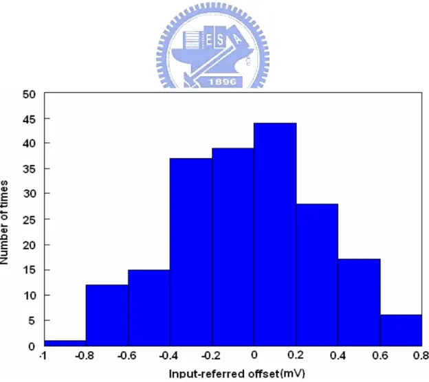
in which p could represent parameters of the device such as width, length, threshold voltage [10]. If we specify the standard deviation of Gaussian distribution well the simulated process variation approaches to the fabricated process variation. The standard deviation is specified according to device parameters of TSMC 0.35um technology. We model only the width of each device as the form in (2.12) and perform 200 Monte Carlo indices. Fig 2.15 shows the offset distributions over 200 Monte Carlo indices. We redraw it as the histogram shown in Fig 2.16 and obtain that the standard deviation of input-referred offset voltage (σ(Vos) ) is 0.34mV and the mean is -0.024mV.
This means that we will have 99.7% of input-referred offset voltage within 3σ(Vos) in fabrication.
Since only the width variation has been modeled the offset is much smaller than what we expect. In general the input-referred offset is dominated mostly by the threshold mismatch of the input differential pairs. Finally, we summarize the performance of telescopic opamp in Tab 2.3.
2.6.2 Bootstrapped Switch Simulated Results
Tab 2.4 shows the sizes of all transistors in bootstrapped analog switch. We see that in Fig 2.17 the gate-source voltage of Mc-vgs remains a constant value. In (2.1) we see clearly that this leads to
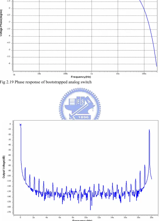
constant charge injection if the body effect is ignored and could be seen in Fig 2.18. In Fig 2.18 charge injection makes the negative voltage change but it is almost independent of voltage level. Fig 2.19 shows the phase relationship between input and output and reveals the almost zero-phase shift up to 20MHz (Nyquist-rate frequency).
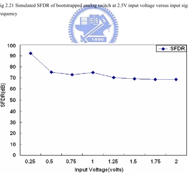
Now we take a look at sampled signal spectral to find the SFDR (Spurious Free Dynamic Range), which is the peak signal in the output spectrum to the largest spike in the output spectrum up to the Nyquist frequency [8]. We will consider two situations: (1) with the highest signal level (2.5V for single-ended), we see output spectrum at different input frequencies. Fig 2.20 shows the output spectrum at input frequency of about 20MHz and we see that SFDR is about 68dB. In constant input signal level of 2.5V, Fig 2.21 illustrates the SFDR values versus input frequency. (2)
at about input frequency of 20MHz, we see output spectrum at different input signal level (single-ended). Fig 2.20 illustrates the SFDR values versus input signal level.
2.6.3 Precharged SHA Simulated Results
The final design of precharged SHA is shown in Fig 2.23 and the remaining NMOS switch sizes are listed in Tab 2.5. For seeing the transient signal curve we use bootstrapped analog switches including S1, S2, S11, S12 to simulate the overall circuit. The simulated input and output signals are
shown in Fig 2.24. Now we consider two situations that S1, S2, S11, S12 are bootstrapped switches
or ideal switches to understand the importance of this analog switch. In the next section the input signal must meet the requirement of:
sin in s M f f = M (2.13)
, where fsis sampling frequency, Msin is prime integer number of sinewave cycles and M is the number
of samples. We take M=1024 samples in the following simulations. For example, if we want to input a signal near 1MHz we can select Msin=23, running 23 cycles of sinewave, to have fin=0.8984375MHz
2.6.3.1 Ideal-Switch Precharged SHA Simulated Results
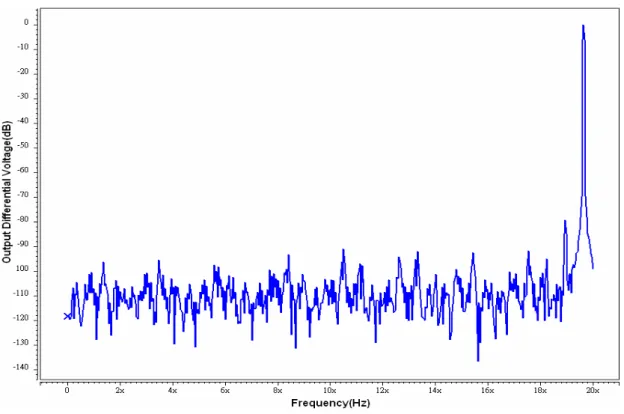
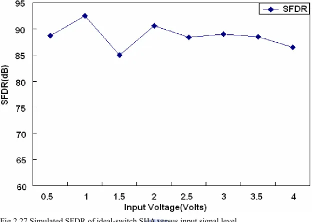
In this section, we will consider the effects of either input signal level or input frequency respectively: (1) with the signal level of 4Vp-p (differential), we see the output spectrum at different input frequencies. Fig 2.25 shows the output spectrum at input frequency of about 20MHz and SFDR is 79dB. Fig 2.26 shows the SFDR values with 4Vp-p input voltage versus input frequency. (2) Fig 2.27 shows the SFDR values at input frequency of 20MHz versus input signal level.
2.6.3.2 Bootstrapped-Switch Precharged SHA Simulated Results
First, we take a look at the output frequency spectrum of SHA with the implementation of real transistors. Fig 2.28 shows a frequency spectrum when 4Vp-p and 20MHz input signal is presented and SFDR is about 73dB. In the same procedure as the last section, we will find out how signal level and frequency affect the SFDR value. (1) shown in Fig 2.29 is the SFDR values with signal level of 4Vp-p versus input frequency. (2) shown in Fig 2.30 is the SFDR values at input frequency of 20MHz versus input signal level.
2.6.4 Final Results and Discussions
The transient simulation in HSPICE doesn’t include the electronic noise, i.e. thermal noise, flicker noise, etc. We must take another way to look at how much noise affects the circuit. By using AC simulation in HSPICE we could integrate the total noise power in the bandwidth we interest. When in the sample mode the simulated RMS input-referred noise voltage up to noise equivalent bandwidth (NEB) is 0.285mV and 0.252mV when in the hold mode. Fig 2.28 shows that electronic-free SFDR is 73.88dB in full-range signal and also means that RMS distortion noise voltage is 0.286mV by using the formula:
( ) ( ) (
2 2)
2 2 20 log p d n off V SFDR V V V = + + (2.14), Vd, Vn and Voff are RMS noise voltages of distortion, electronic noise and offset due to process
variations respectively and Vp is an amplitude of a sinewave [9]. Now it is intuitive to add these
three noise powers together to obtain that the final electronic-included SFDR of SHA is 69.45dB [14].
The circuit is affected by many noise sources. Like those we presented are nonlinearity of devices and electronic noise. We should notice that the signal level and its frequency will provide the noise of nonlinearity because the transistors in opamp may be pushed into the triode region. The electronic noise is independent of signal level and should be concerned in another way to really characterize the circuit performance by simulation. Finally, we use Tab 2.6 to summarize the performance of precharged SHA.
Fig 2.3 CMOS switch configuration
Fig 2.5 Precharged SHA configuration
Fig 2.7 Telescopic opamp with continuous-time common mode feedback (CMFB) circuit
Fig 2.9 Bootstrapped analog switch configuration
Fig 2.11 Channel resistance of Mc-vgs in bootstrapped analog switch versus input signal level
Fig 2.13 Input/Output transfer curve of telescopic opamp
Fig 2.15 Simulated input-referred offset voltage over 200 Monte Carlo indices
Fig 2.17 Control and input signals of bootstrapped analog switch
Fig 2.19 Phase response of bootstrapped analog switch
Fig 2.20 Frequency spectrum of bootstrapped analog switch when 2.5V and 20MHz single-ended input signal is presented
Fig 2.21 Simulated SFDR of bootstrapped analog switch at 2.5V input voltage versus input signal frequency
Fig 2.23 Precharged SHA with real transistor implementation, where the bootstrapped analog switches are shown in Fig 2.9
Fig 2.25 Frequency spectrum of ideal-switch SHA at frequency of 20MHz and differential input of 4Vp-p
Fig 2.27 Simulated SFDR of ideal-switch SHA versus input signal level
Fig 2.28 Frequency spectrum of bootstrapped-switch SHA at input frequency of 20MHz and differential input of 4Vp-p
Fig 2.29 Simulated SFDR of bootstrapped-switch SHA versus input signal frequency
Capacitor Value (KT/C)1/2 (T=343k) 0.1p 0.218mV 0.2p 0.154mV 0.4p 0.109mV 0.6p 0.089mV 0.8p 0.077mV 1p 0.069mV Tab 2.1 RMS noise voltage on a capacitor
Transistor Size Multiple
M1=M2 L=0.4u W=3u m=10 M3=M4 L=0.5u W=3u m=1 M5=M6 L=0.35u W=2u m=10 M7=M8 L=2u W=5u m=8 Mc1=Mc2=Mc3=Mc4 L=0.35u W=2u m=4 Mcb1=Mcb2 L=2u W=5u m=4 Mc5 L=2u W=2u m=5 Ms L=2u W=4u m=10
Tab 2.2 Transistor sizes of telescopic opamp
Specifications Performance
DC Gain 552
Unity-Gain Frequency 590MHz (CL=0.25p)
Phase Margin 67 (CL=0.25p)
Input Common Mode Range 0.8V (0.85V~1.65V)
Output Swing 1.2V (-0.6V~0.6V)
Input-Referred Offset Voltage σ(Vos)=0.34mV
Supply Voltage 3V
Power Consumption 2.72mW
CMOS Technology TSMC 2P4M 0.35um
Transistors Size Multiple M9n L=0.35u W=1u m=1 M9P L=0.35u W=1u m=4 M10n L=0.35u W=1u m=1 M10p L=0.35u W=1u m=4 M11 L=0.35u W=1u m=1 M12 L=0.35u W=1u m=1 M13 L=0.35u W=1u m=6 M14 L=0.35u W=1u m=6 M15 L=0.35u W=1u m=4 M16 L=0.35u W=1u m=4 Mc-vgs L=0.35u W=1u m=40
Tab 2.4 Transistor sizes of bootstrapped analog switch
Switch Type Size
S1=S2=S11=S12 Bootstrapped switch Listed in Tab 2.4
S3=S4 NMOS L=0.35u W=2u
S5 NMOS L=0.35u W=2u
Tab 2.5 Switch sizes of precharged SHA
Specifications Performance
Sample Rate 40MHz
SFDR @ fin=20MHz and Vin=4Vp-p 69.45dB (including electronic noise)
Differential Input 4Vp-p
Supply Voltage 3V
Power Consumption 3.02mW
CMOS Technology TSMC 2P4M 0.35um
CHAPTER 3
Multiplying Digital-to-Analog Converter
3.1 Introduction to Multiplying Digital-to-Analog Converter (MDAC)
MDAC performs the function of quantification after signals are sampled. There are so many methods to quantize the analog signals and MADC is frequently used in pipelined ADC since it has advantages of low power and high speed. Recall that from Chapter 1 we listed the method that if we solve multiple bits in the first stage of pipelined ADC, then we could achieve low power circuit but may slow it down. To determine the numbers of bits solved in the first stage is a strong tradeoff between power and speed. A lot of designs would keep the design to be simple and radix-2 1.5-bit MDAC illustrated in Fig 3.1 is used to perform medium resolution and high speed [7]. We should note that solving multiple bits in the first stage does not always let the entire system be low power, since analog circuit therefore would be very difficult and even impossible to design. There are some properties we should know about radix-2 1.5-bit MDAC: (1) higher speed is required for opamp since the feedback factor (f=1/2) is small when amplification is two. (2) long latency for signals to pass through since we need 10 stages to perform 10-bit ADC. (3) small capacitors array are needed since the capacitors shown in Fig 3.1 are equal for amplification of two. (4) large numbers of opamps are needed since for a given resolution of ADC, each stage just solving one bit actually leads to 10 stages, i.e. ten opamps, if opamp sharing is not used.
In Fig 3.1 we see that we need the circuit components consisting of comparators, opamps and digital encoder. The following sections will show the design of these circuit components.
3.2 Differential Comparator Design
3.2.1 Differential Comparing Circuit Design
differently, -1V (Vref+=0.5V, Vref-=2.5V) and 1V (Vref+=2.5V, Vref-=0.5V) respectively. Fig 3.2 shows the differential comparing circuit with the equivalence of four capacitors and performs the function described by the following equation:
/ 2
o i ref
V
= −
V V
(3.1) ,which can be derived by the fact of charge conservation in two clock phases [7]. In ψ3 phasethe circuit is connected like the one shown in Fig 3.3(a), in which reference voltages are sampled on capacitors. When in ψ1 phase the configuration change to connect input nodes to signals like
the one shown in Fig 3.3(b). Then the charge will redistribute and lead to the output voltage in (3.1).
Capacitor sizes are chosen by considering KT/C noise (Tab 2.1), which must be smaller than 1 LSB when noises in each phase are added. For large signal to be passed, all of the switch symbols in Fig 3.2 are replaced by CMOS switches and is illustrated in Fig 3.4. When in ψ3 phase CMOS
switches sizes are chosen according to Fig 3.3(a) to make sure that reference voltages are stable for a given time. When in ψ1 phase it follows the same way to determine the sizes of switches,
but we should note that the charge injections are not the issue because the nodes X and Y see the high impedances.
3.2.2 Preamplifier Design
Now we continue to see the following two stages shown in Fig 3.5. In this figure the first stage is a simple differential amplifier with active loading. It is used to provide gain to enhance the input of latch for avoiding metastable problem [15]. It also can reduce the input-referred offset of latch and kickback noise [16][17]. Notice that the -3-dB frequency must be higher than input frequency and the gain should also have its proper value in order to tolerate temperature and process variations. The purpose with loading consisting of four p-type transistors is to ease the design of size for a given current [8], and essentially gm15 and gm16 should be smaller than gm13 and
3.2.3 Latch Design
The second stage in Fig 3.5 called latch is used to generate the digital outputs when M17 and M18 have unbalanced voltages apply to them. We should note that this action occurs when ψ1ba is
going high, so it acts like positive edge trigger. The latch is very sensitive to random mismatches coming from process variation, so transistor sizes must be chosen carefully for small process variation, i.e, the larger size. Fortunately, radix-2 1.5-bit MDAC can tolerate 500mV (Vref/4) offset voltage if digital error correction circuit is used to combine comparator’s outputs [7][9].
3.3 Opamp Design
The two-stage opamp used in MDAC is shown in Fig 3.6. The main consideration here is that the output swing has to be at least 2Vp-p at each single side, so the second stage is mainly used to help increase the output swing. When designing the two-stage opamp the most difficult part is the compensation between the tradeoff of unity gain frequency and phase margin and also makes these two specifications reasonable. It is much easier to compensate when the first stage has cascode configuration. It is shown in Fig 3.6 that the compensation capacitors are connected between outputs and the sources of cascode transistors in order to eliminate the right-hand-plane (RHP) zero [18][19]. Now we move to determine some specifications of opamp to achieve the requirements. By seeing the configuration like Fig 3.7 we could use the equation written as:
1
1
f s f s p f fC
C
C
C
C
G
C
A
C
+
⎛
+
+
⎞
=
⎜
−
⎟
⎝
⎠
(3.2) to estimate the requirement of opamp’s DC gain. For close-loop gain accuracy being within 0.5 LSB we must meet the inequality written as:1
1
1
2
f s p N fC
C
C
A
C
++
+
≤
(3.3) For the left term of this inequality to be smaller than 0.5 LSB, we can easily obtain that the gain of 73dB is required when Cf=Cs=5Cp and N=10 are assumed. We then use the equations written as:1
1
2
2
f s p t t fC
C
C
f
f
C
τ
π β
π
+
+
⎛
⎞
=
=
⎜
⎟
⎝
⎠
(3.4) 3 11
2
T Ne
φτ
≤
+ (3.5) , where Tψ3is the period when ψ3 is high and β is the feedback factor. The settling accuracy should be less than 0.1% of sampled voltage. Using (3.4), (3.5) to calculate the time constant needed for 0.1% settling accuracy and we obtain that unity gain frequency (ft) of 443MHz isrequired. We must notice that the beginning of settling behavior is nonlinear and is called the slew behavior. This means that the overall settling time includes both slew and small signal behaviors. The slew rate is written as:
Iss
SR
Cc
=
(3.6) , where Iss is the current flowing in Ms and Cc is the compensation capacitor. The higher the slewrate, the faster the speed that the circuit enters the small signal behavior, but just a waste of power. The common mode feedback (CMFB) circuit is shown in Fig 3.8 [20]. When the circuit is stable, in ψ3 phase the desired voltage is stored on C3 and C4 and the opamp is performing its
amplification. When in ψ1 phase the charge is then shared with C1 and C2 and keep the output
voltages as desirable common mode voltages. In this figure Mcmc denotes MS and M9, M10 shown
in Fig 3.6. Mcmc should be sized properly to accommodate the sum of currents flowing in current
sources. The output common mode voltages are chosen by considering opamp’s DC characteristics, the two output common mode voltages chosen are also shown in Fig 3.6 (2V and 1.5V for the two stages respectively).
3.4 MDAC Design
Fig 3.9 shows the entire MDAC structure. The phase arrangement seems complicated and easily confused designers. We focus on phase arrangement first. Fig 3.10 shows the three phases used in MDAC. The ψ is used to positively trigger the comparators. It should be ensured that the
outputs of encoder come out after ψ1 is going low. When in ψ1 phase voltages sampled on Cf
and Cs and in ψ3 phase the subtraction voltages (controlled by encoder) together with opamp and feedback capacitor Cfwill operate the function written as:
1 1 1 1 1 s s f s j j os f f f s C C C C V V Vr V C C C C + + ⎛ ⎞ = + − + +⎜ ⎟⋅ ⎝ ⎠ +
⎛
⎞
⎛
⎞ ⎜
⎟
⎜
⎟ ⎜
⎟
⎝
⎠
⎝
⎠
(3.7), in which the subtraction voltages Vr=-4V, 0V, 4V depend on which segment Vj locates, and Vos is the input-referred offset of opamp. We use Fig 3.11 to graphically illustrate the transfer function, where the dividing lines are at -1V and 1V (comparator’s threshold voltage). We also see that the matching of these two capacitors is important. According to Fig 3.11 and ignore the offset voltage we can write the general form of MDAC’s transfer function as:
( )
1 da j j j j j
V
+=
G
×
⎡
⎣
V V
−
D
⎤
⎦
(3.8) , where Gj is the gain of MDAC and Vjda(Dj) is the analog signal (-2V, 0V, 2V) corresponding to digital codes coming out of comparators. The linearity of MDAC is influenced the most by opamp while the switches are not much the issue. Making lots of efforts on designing opamp will improve MDAC’s performance and will be simulated in the next few sections.3.5 Simulated Results
3.5.1 Differential Comparator Simulated Results
The sizes of transistors in comparator are shown in Tabs 3.1 and 3.2. First we should know how to set the reference voltage. In (3.1) we know that the threshold voltage is (Vref+-Vref-)/2. The output of the stage in Fig 3.2 satisfies (3.1). Fig 3.12(a) and Fig 3.12(b) are the simulated results that show the input /output transfer curve when threshold voltages are 1V and -1V respectively.
There is an important issue we should concern about, speed. The overdrive recovery is the ability that the comparator’s output should be changing fast enough when input signal level has
large amplitude transition [13]. Now we let the Vref+=2.5V and Vref-=0.5V, so the threshold voltage is 1V (Vref/2). Base on this initial setting we inputs the discreet-time signal sequence: {2V, 0.99V, 2V, 0.99V, -2V, 1.01V, -2V, 1.01V}, then we should obtain the digital output sequence: {1, 0, 1, 0, 0, 1, 0, 1}. Fig 3.13 shows the simulated waveforms which meet the requirement stated above.
3.5.1.1 Input-Referred Offset Voltage Simulation
The comparator is very sensitive to process variation although it is not much the issue in this design. The process variation would make the threshold voltage deviate seriously. Make sure that 3σ(Vos) is a tolerable value is important. To simulate the offset voltage we also only model all the
widths of the transistors and values of capacitors with variations in the form of Gaussian distribution. A little different from what we did in the last chapter is that we have to see the transient behavior in each Monte Carlo index. First we set the threshold voltage at 1V and input a constant voltage (assuming 0.99V) during the hold mode of SHA, then we simulate 600 Monte Carlo indices to see how many times the output is digital one. There is an assumption that the input-referred offset voltage has Gaussian distribution with mean of 1V and unknown standard deviation. Fig 3.14 is the histogram of simulated output voltages, where we have 31.12% of samples are digital one.
We use X~P(μ,σ2)=P(1v, σ2) to denote the statements above, where σ is the standard deviation we want to obtain. Now we have P(X<0.99V)=0.3112. In order to consult the standard normal distribution table we should standardize P(X<0.99V)=0.3112 to P[Z<(0.99v-1V)/σ]=0.3112 [21]. We then consult the table reversely, and obtain that the probability of 0.3112 lies in the range of -0.5<Z<-0.49. We choose -0.495 for simplicity. Then we can easily solve the equation of (0.99V-1V) /σ =-0.495 to obtain that σ=20.2mV. Tab 3.3 is the summary of the comparator’s performance.
Tab 3.4 shows the transistor sizes of two-stage opamp and Tab 3.5 shows the switch sizes of CMFB. Fig 3.15 shows the frequency response of opamp. The dc gain of 5887 (75dB), unity gain frequency of 484MHz and phase margin of 70 degree can be read. Fig 3.16 shows the input common mode range by simulating the transconductance (gm) of input differential pairs. In this
figure we see that the transconductance is much stable between 1.2V and 1.8V.
Fig 3.17 shows the settling behavior by inputting a voltage pulse when the unity feedback is formed. This figure tells that the slew rate is about 0.3V/ns and it takes about 5ns including slew and small signal behavior for 0.1% settling accuracy. Since the dynamic CMFB is used, the output common mode voltage is seen in Fig 3.18 by transient simulation. We can clearly see the voltage settling behavior and that its final stable voltage is 1.487V.
Now we model each transistor’s size as Gaussian distribution to simulate the offset voltage. When there is no input signal the output differential voltage should be zero except that process variation exists. By simulating 200 Monte Carlo indices we can see 200 windows like the one shown in Fig 3.18 (where both the output voltages are 1.487V so the differential voltage is 0V) except that the stable differential voltage is not zero. We sample 200 stable voltages in these 200 windows and plot it as a histogram in Fig 3.19. In Fig 3.19 the standard deviation of output offset voltage is 0.61V and mean is -8mV. If what we want is input-referred offset voltage we divide it by DC gain of this opamp by ensuring that the outputs haven’t saturated in advanced. The standard deviation of input-referred offset voltage is then 0.104mV. This offset voltage is not the issue because in (3.7) we see that it just be amplified by two. Finally we use Tab 3.6 to summarize the performance of two-stage opamp.
3.5.3 MDAC Simulated Results
The MDAC is the system that processes the discreet-time signals. If we put the stairs-like voltage from -3V to 3V, we will get the output voltage we want like Fig 3.11. Tab 3.7 shows the switch sizes of MDAC. The simulated output of MDAC is shown in Fig 3.20 and it is pretty like a
one shown in Fig 3.11. If we want to see how the output of MDAC will be when sinewave signal entering the SHA, we connect two stages including SHA and the first stage of MDAC like the one shown in Fig 3.21 and use an ideal switch modeled by HSPICE to sample the settled signals (SW is
high when MDAC’s outputs are settled). Fig 3.22 shows the simulated waveform at ideal switch’s (SW) output and it is consistent with the function shown in Fig 3.20. Now we should continue to
check that whether the step heights in each step are equal or not. The equality of step heights means good linearity of the MDAC. Let us assume that no mismatch is presented and rewrite (3.8) if some noise and distortion are involved, then it can be written as:
(
)
1
( )
os.
j j j j j
V
+=
V Vr D
−
−
V
G
(3.9) , where Vjos means an unwanted noise including process variation, electronic noise and devicesnonlinearity (in HSPICE transient simulation the electronic noise has not been included) and Gj is
still two since we lump all the noises into Vjos. Solving Vjos in (3.9) and renames it by INL, then
we got: 1
( )
j j j jV
INL
Vr D
V
G
+∧
⎛
⎞
⎜
⎟
=
+
−
⎜
⎟
⎝
⎠
(3.10) 1 jV
∧
+ ’s are the simulated outputs in Fig 3.20. Fig 3.23 shows the values obtained from (3.10) and they are called integral-non-linearity (INL) error. We see that INLmaxis 0.25 LSB and INLmin is -0.32 LSB. Generally, the INL errors less than 0.5 LSB are tolerable values.Fig 3.1 A radix-2 1.5-bit switch-capacitor pipeline stage configuration
(a) (b)
Fig 3.3 Circuit connection in two phases (a) Sample the reference voltages on capacitors (b) Sample the signal voltages on capacitors
Fig 3.5 Preamplifier and latch configurations
Fig 3.7 Simplicity of a differential ×2 amplifier used for understanding the gain and speed requirements of opamp
Fig 3.9 MDAC configuration
Fig 3.11 Transfer curve of MDAC
(a)
(b)
Fig 3.13 Digital output of comparator when input is a certain signal pattern
Fig 3.15 Gain response and phase response of two-stage opamp
Fig 3.17 Transient simulation when unity-gain feedback is connected
Fig 3.19 Simulated output offset voltage of two-stage opamp over 200 Monte Carlo indices
Fig 3.21 Block diagram for catching the settled signal of MDAC’s output
Fig 3.23 INL error of MDAC’s transfer function
Switch Type Size
S1, S2, S3, S4 CMOS NMOS:L=0.35u W=10u
PMOS: L=0.35u W=40u
S5 NMOS L=0.35u W=4u
Tab 3.1 Switch sizes of comparing circuit
Transistor Size Multiple
M11=M12 L=0.35u W=2u m=12 M13=M14 L=0.35u W=0.5u m=8 M15=M16 L=0.35u W=0.5u m=7 M17=M18 L=0.35u W=2u m=2 M19=M20 L=0.35u W=2u m=1 M21=M22=M23=M24 L=0.35u W=2u m=2 M25 L=1u W=2u m=6 M26 L=1u W=2u m=6