國 立 交 通 大 學
電機學院微電子奈米科技產業研發碩士班
碩 士 論 文
在有機薄膜電晶體低溫製程下利用常壓式電漿技
術沉積閘極二氧化矽
Low Temperature Processes of Organic Thin-Film Transistor
with Gate Dielectric of Silicon Dioxide Deposited by Scanning
Atmospheric-Pressure Plasma Technology
研 究 生 : 吳 永 茂
指導教授 : 張 國 明 博士
在有機薄膜電晶體低溫製程下利用常壓式電漿技
術沉積閘極二氧化矽
Low Temperature Processes of Organic Thin-Film Transistor
with Gate Dielectric of Silicon Dioxide Deposited by
Scanning Atmospheric-Pressure Plasma Technology
研 究 生: 吳永茂 Student: Yung-Mao Wu
指導教授: 張國明 博士 Advisor:Dr. Kow-Ming Chang
國 立 交 通 大 學
電機學院微電子奈米科技產業研發碩士班
碩 士 論 文
A Thesis
Submitted to College of Electrical and Computer Engineering National Chiao Tung University
in partial Fulfillment of the Requirements for the Degree of
Master In
Industrial Technology R & D Master Program on Microelectronics and Nano Sciences
January 2008
Hsinchu, Taiwan, Republic of China
i
在有機薄膜電晶體低溫製程下利用常壓式電漿技
術沉積閘極二氧化矽
研究生: 吳永茂 指導教授: 張國明 博士
國立交通大學電機學院產業研發碩士班
摘要
我們已經成功地利用大氣壓電漿技術在有機薄膜電晶體低溫製程下沉積閘極 矽氧化物,大氣壓電漿技術的優點是可以在一般正常氣壓下沉積矽氧化物,並且 也可以應用在低溫製程下適合軟性電子製程條件,在這次研究中,我們的有機薄 膜電晶體操作電壓小於-5 伏特,利用 MIM 的結構量出絕緣層在 0.5 MV/cm 的崩潰 電場下漏電流大約在 9×10⁻⁸ A/cm2 ,在可携式的電子產品上低的操作電壓與低的漏 電流是必要的條件,對於沒有定義有機半導體的主動成區域比有定義有機半導體 的主動層區域的漏電流特性大,而且對於有沉積 HMDS 的元件比沒有沉積 HMDS 的 元件的漏電流特性大。
ii
Low Temperature Processes of Organic Thin-
Film Transistor with Gate Dielectric of Silicon
Dioxide Deposited by Scanning Atmospheric
-Pressure Plasma Technology
Student: Yung-Mao Wu Advisor: Dr. Kow-Ming Chang
Industrial Technology R & D Master Program of
Electrical and Computer Engineering College
National Chiao Tung University
ABSTRACT
We have successfully fabricated pentacene-based organic thin film transistor at a low temperature process with silicon oxide as a gate dielectric deposited by atmospheric-pressure plasma technology (APPT). The major merit of scanning atmospheric-pressure plasma technology was low deposition temperature at one standard atmosphere which was suitable for the application of flexible electrons. The organic thin film transistor demonstrated in this study could operate at the voltage less than -5V and the leakage current of silicon oxide dielectric with MIM structure is about 9×10⁻⁸A/cm2 at 0.5 MV/cm. The low operation voltage and low leakage current properties are required in portable applications. Leakage current of not define pentacene region is higher than define pentacene region. And leakage current of have HMDS is higher than not have HMDS.
iii
誌 謝
首先,要感謝的是我的指導老師張國明教授,在這兩年的碩士研究生涯裡給 予熱心的指導和教誨,使的我不論在研究上或待人處事上都有很大的收穫,更給 我們建立獨立思考解決問題的觀念,也不斷的激勵我,讓我更有信心的完成我的 學業,在此衷心的表達感謝之意。 再來,我要感謝知添學長、俊銘學長、建宏學長、伯寧學長及明峯學長的建 議及協助,謝謝各位學長在研究上所提供的意見和幫助,讓我增廣不少專業領域 的知識,此外更感謝士軒學長對我的教導和鼓勵,讓我得以順利完成實驗並順利 的完成碩士學業。 接下來我還要感謝的是實驗室的同學,明紳、文全、勝軍、明聰、鈞凱、菘 宏、明頤、詩帆、庭嘉、彥忠。有了各位,才讓我的研究生活充滿歡樂與色彩, 使的實驗室除了是研究的地方之外更是充滿溫情歡笑的地方,很高興與各位度過 這美好的時光,做實驗有你們的相伴,讓我倍感溫馨,感謝大家的鼓勵與支持, 謝謝你們。 另外,我要感謝好友信翰及建邦的幫助和砥礪,你們是很有熱忱的人,讓我 學到很多如何建立良好的人際關係,在研究期間結交不少彼此互助的益友,謝謝 你們。 最後,我要感謝我的家人林東美先生與吳碧霞女士,還有兄弟姊妹給了我最 大的支持和鼓勵,因為有你們溫馨的關懷,讓我覺得一切都過的很豐富,有了你 們的支持與栽培,才有今日順利完成自己的理想,感謝這一切所帶來的美好。
iv
Contents
Chinese Abstract
………..………iEnglish Abstract
………...iiAcknowledgement (in Chinese)
...iiiContents
……….………....ivTable Captions
………...………...viFigure Captions
………...…………...…....viiChapter 1 Introduction
1.1 Application and Motivation of Organic Thin Film Transistor (OTFT)……...11.2 Issues for fabrication OTFT structures……….………...….2
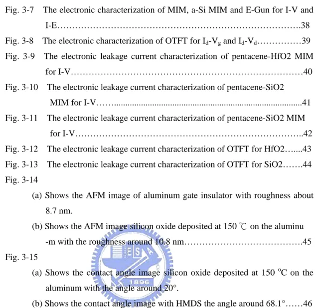
1 . 2 . 1 O r g a n i c s e m i c o n d u c t o r m a t e r i a l … … … . … … . . . 3 1 . 2 . 2 S o u r c e / D r a i n c o n t a c t … … … . … … . … . . 5 1 . 2 . 3 H i g h d i e l e c t r i c c o n s t a n t i n s u l a t o r … … … . … … … . . . 5 1 . 2 . 4 A c t i v e r e g i o n p a t t e r n … … … . … … … . … … . … . 6 1 . 2 . 5 P a s s i v a t i o n … . . … … … . . … … … . … . . … . . 6 1 . 2 . 6 S u r f a c e t r e a t m e n t … … … . . … … … . . … . . 7 1 . 2 . 7 D e v i c e t r e a t m e n t … . … … … . . … … … . . . . 7
1.3 Gate dielectric for organic and inorganic materials ……...………...8
1.4 Introduction of APPT ….………..…………..………….….….…..9
1.5 Thesis Organization…..………..………10
Chapter 2 Experiment
2.1 Silicon oxide deposited with E-gun and SAPPT equipments on the metal insulator semiconductor (MIS) structure………..………….………….…..172.2 Silicon oxide deposited with effect of substrate temperature by SAPPT on the metal insulator metal (MIM) structure………..……..….…..…………..…17
2.3 Deposition of silicon oxide dielectric under room temperature on amorphous silicon metal insulator metal (a-Si MIM) structure……...……..……..…...18
2.4 Fabricated processes of organic thin film transistor (OTFT)…………...….19
v
Chapter 3 Results and Discussion
3.1Silicon oxide dielectric layer quality analysis and appraisal…..…..……..…27 3.1.1 MIS………..…..……….…..………27 3.1.2 MIM…………..………...……….………28 3.1.3 a-Si MIM…………...….………..……….…28 3.2 Determination of Threshold voltage and Mobility…………..…..…….……29 3.3 OTFT electric characteristics analysis and discussion………..………..…...29 3.4 Leakage current characteristic of OTFT discussion in various structures.…30
Chapter 4 Conclusion
4.1 Conclusions…..………..………47 4.2 Future work………..…..………48
vi
Table Caption
Chapter 1
Ta b l e 1 - 1 : C o m p a r e w i t h characterization f o r a v a r i e t y o f f l e x i b l e e l e c t r o n i c s u b s t r a t e s … … … . . 11 Ta b l e 1 - 2 : Characterization of materials for OTFT………12 Ta b l e 1 - 3 : Characterization of contact angle for organic and inorganic mate-rials………..15 Ta b l e 1 - 4 : Characterization of dielectric materials and process methods for
vii
Figure Caption
Chapter 1
Fig. 1-1 C o m p a r e w i t h temperature f o r a v a r i e t y o f f l e x i b l e e l e c t r o n i c s u b s t r a t e s … … … . 1 1 Fig. 1-2 Construction of o r g a n i c t h i n - f i l m t r a n s i s t o r s … … … . . 1 2Fig. 1-3 Classification of semiconductor materials……….13
Fig. 1-4 Molecular structure of pentacene………...13
Fig. 1-5 Molecular structures of P3HT and BBL………13
Fig. 1-6 Influence of mobility for OTFT passivation………..14
Fig. 1-7 The electrical characteristics of OTFT encapsulated by the PVA coating method………...14
Fig. 1-8 The electrical characteristics of OTFT encapsulated by polyacrylate -based adhesive multilayer composed method………..14
Fig. 1-9 Schematic of the organic thin film transistors (OTFTs) with (a) Top gate/Bottom contact structure (b) Top gate/Top contact structure (c) Top contact/Bottom gate structure (d) Bottom contact/Bottom gate structure (e) Double gate structures………...15
Fig. 1-10 APPT system of ITRI………16
Chapter 2
Fig. 2-1 Fabrication flow of metal insulator semiconductor (MIS)……….21Fig. 2-2 Fabrication flow of metal insulator metal (MIM)………...23
Fig. 2-3 Fabrication flow of amorphous silicon metal insulator metal (a-Si MIM).24 Fig. 2-4 Fabrication flow of organic thin film transistor (OTFT)………26
Chapter 3
Fig. 3-1 The electronic characterization of MIS………..32Fig. 3-2 The electronic characterization of MIM for C-V and I-V………..33
Fig. 3-3 The electronic characterization of MIM for I-V and I-E………34
Fig. 3-4: The electronic characterization of a-Si MIM for C-V and I-V……….35
Fig. 3-5 The electronic characterization of a-Si MIM for I-V and I-E……….36
Fig. 3-6 The electronic characterization of MIM, a-Si MIM and E-Gun for C-V and I-V………...37
viii
Fig. 3-7 The electronic characterization of MIM, a-Si MIM and E-Gun for I-V and I-E……….38 Fig. 3-8 The electronic characterization of OTFT for Id-Vg and Id-Vd………39
Fig. 3-9 The electronic leakage current characterization of pentacene-HfO2 MIM for I-V………40 Fig. 3-10 The electronic leakage current characterization of pentacene-SiO2
MIM for I-V……...41 Fig. 3-11 The electronic leakage current characterization of pentacene-SiO2 MIM for I-V………..42 Fig. 3-12 The electronic leakage current characterization of OTFT for HfO2…....43 Fig. 3-13 The electronic leakage current characterization of OTFT for SiO2…….44 Fig. 3-14
(a) Shows the AFM image of aluminum gate insulator with roughness about 8.7 nm.
(b) Shows the AFM image silicon oxide deposited at 150 ℃ on the aluminu -m with the roughness around 10.8 nm……….45 Fig. 3-15
(a) Shows the contact angle image silicon oxide deposited at 150 oC on the aluminum with the angle around 20°.
1
Chapter 1
Introduction
1.1 Application and Motivation of Organic Thin Film Transistor ( OTFT )
I n t h e p a s t d e c a d e , o r g a n i c t h i n - f i l m t r a n s i s t o r ( O T F T ) h a s b e e n s t u d i e d e x t e n s i v e l y. N o w, t e c h n i c a l p r o d u c t g r a d u a l l y m o r e a n d m o r e p r o g r e s s , f r o m l a r g e t o s m a l l a n d f r o m w e i g h t t o l i g h t , p e o p l e ' s l i f e i s m o r e a n d m o r e c o n v e n i e n t i n e m p h a s i z e s h i g h e f f i c i e n c y c e n t u r y. A l o n g w i t h t h e l o w c o s t a n d t h e m a s s i v e l y m a n u f a c t u r e s t e c h n o l o g y, t h e e l e c t r o n i c p r o d u c t s m a r k e t s t a r t s t o e m p h a s i s , o r g a n i c t h i n f i l m
t r a n s i s t o r s start to become the research the tidal current. No matter industry or academia
energetically investment research.
E x c e p t c o n v e n t i o n a l t e c h n o l o g y o f d i s p l a y o n g l a s s s u b s t r a t e , t e c h n o l o g y o f d i s p l a y o n f l e x i b l e s u b s t r a t e a l r e a d y b e c o m e s n o t i c e a b l e t e c h n o l o g y o n n e x t g e n e r a t i o n . O r g a n i c t h i n f i l m t r a n s i s t o r s h a v e a l r e a d y m a n u f a c t u r e d o n f l e x i b l e s u b s t r a t e f o r l o w c o s t a n d l o w t e m p e r a t u r e p r o c e s s . I n a t p r e s e n t , s o m e m a n y f l e x i b l e s u b s t r a t e s a r e r e s e a r c h e d a n d d e v e l o p e d , s h o w f i g u r e 1 - 1 . P o l y ( e t h y l e n e t e r e p h t h a l a t e ) ( P E T ) a n d p o l y ( e t h y l e n e n a p h t h a - l a t e ) ( P E N ) w e r e o f t e n u s e d f o r O T F T s u b s t r a t e s . B e c a u s e , t h e y h a v e v e r y l i t t l e e f f e c t o n t h e m e l t i n g p o i n t ( T m ) , w h i c h i n c r e a s e s b y o n l y a f e w d e g r e e s b u t a s u b s t a n t i a l e f f e c t o n t h e g l a s s t r a n s i t i o n t e m p e r a t u r e ( T g ) . M o r e o v e r, c h o o s e s t h e s u i t a b l e m a t e r i a l o f s u b - s t r a t e i s i m p o r t a n t , v i e w t a b l e 1 - 1 . We w i l l s e t e x p e r i m e n t a l p r o c e s s t e m p e r a t u r e l e s s t h a n 3 0 0℃. H o w e v e r, o r g a n i c t h i n f i l m t r a n s i s t o r s h a v e m o r e p o t e n t i a l t h a n c o n v e n t i o n a l t r a n s i s t o r s . O r g a n i c t h i n f i l m t r a n s i s t o r s h a v e b e e n p r o p o s e d f o r u s e i n v a r i o u s a p p l i c a t i o n s i n d i s p l a y s a n d f l e x i b l e e l e c t r o n i c d e v i c e s . S u c h a s a c t i v e - m a t r i x e m i s s i v e a n d r e f l e c t i v e d i s p l a y s , c h e m i c a l a n d m e c h a n i c a l s e n s o r s , l o w - c o s t f l e x i b l e
2 i n t e g r a t e d c i r c u i t s , r a d i o - f r e q u e n c y i d e n t i f i c a t i o n ( R F I D ) , l i g h t - w e i g h t l a r g e - s c r e e n d i s p l a y s , l o w p o w e r c o n s u m p t i o n , l o w t e m p e r a t u r e m a n u f a c t u r i n g , l i q u i d - c r y s t a l f l a t p a n e l d i s p l a y s , b i o c h e m i c a l s e n s o r s a n d l a r g e - a r e a s e n s o r a r r a y s a n d s o o n . T h e o r g a n i c m a t e r i a l m a y c a r r y o n t h e l a r g e a r e a u s i n g t h e s o l u t i o n t o s p i n - c o a t i n g , o r s e m i c o n d u c t o r t h i n f i l m l a y e r s w e r e d e p o s i t e d b y v a c u u m e v a p o r a t i o n , d o w n t o r e d u c e s t h e m a n u f a c t u r e p r o c e s s t h e c o s t . T h e r e f o r e , i m p r o v e s t h e o r g a n i c t h i n f i l m t r a n s i s t o r t h e m a n u f a c t u r e p r o c e s s t o e n h a n c e t h e m a n u f a c t u r e p r o c e s s e f f i c i e n c y. S u c h a s d i p c o a t i n g , i n k j e t p r i n t i n g a n d c o n t a c t c o a t i n g . N e v e r t h e l e s s , t h e s e a l l a r e s u i t a b l e o n p l a s t i c s u b s t r a t e , O r g a n i c t h i n f i l m t r a n s i s t o r s w i l l d e v e l o p r o l l t o r o l l m a n u f a c t u r e p r o c e s s r e g a r d i n g t h e f u t u r e t o h a v e t h e v e r y l a r g e h e l p . D o w n t o a c h i e v e s m a n u f a c t u r e t h e p r o c e s s s i m p l e a s p i r a t i o n a n d d e v i c e s o f q u a l i t y f r i v o l o u s c h a r a c t e r i s t i c . O n t h e o t h e r h a n d , t h e o r g a n i c s e m i c o n d u c t o r m a t e r i a l i m p r o v e m e n t c h a r a c t e r i s t i c , t h e p r o c e s s e n h a n c e s t h e t e c h n o l o g y a n d t h e O T F T i m p r o v e m e n t s t r u c t u r e , t h e O T F T a p p l i c a t i o n g r a d u a l l y i s r e a l i z e d o n i n t e g r a t e d c i r c u i t s . O T F T d e c i d e s t h e p e r f o r m a n c e o f t h e t r a n s i s t o r b y m o b i l i t y m a g n i t u d e . H o w e v e r, t h e h i g h o p e r a t i n g v o l t a g e r e m a i n s a l i m i t a t i o n o n o r g a n i c t r a n s i s t o r s . O n e o f t h e m o s t c r i t i c a l p r o b l e m s w i t h t r a d i t i o n a l o r g a n i c T F T i s t h e l a r g e o p e r a t i n g v o l t a g e w h i c h i s o f t e n h i g h e r t h a n 1 0 V. T h e r e f o r e , a c c o u n t f o r t h e p o w e r c o n s u m p t i o n o f t h e t r a n s i s t o r t o i n c r e a s e a n d t h e p e r f o r m a n c e o f t h e t r a n s i s t o r t o r e d u c e .
1.2 Issues for fabrication OTFT structures
H o w e v e r, i n o r d e r t o s u c c e s s f u l l y i n t e g r a t e o r g a n i c t h i n - f i l m t r a n s i s t o r s ( O T F Ts ) t e c h n o l o g y, construction of o r g a n i c t h i n - f i l m t r a n s i s t o r v i e w f i g u r e 1 - 2 , t h e r e a r e a f e w i m p o r t a n t i s s u e s t o b e d i s c u s s e d , a s b e l o w s e v e r a l t e r m s :
3
1 . 2 . 1 O r g a n i c s e m i c o n d u c t o r m a t e r i a l
T h e s e m i c o n d u c t i n g m a t e r i a l s g e n e r a l l y d i v i d e i n t o t h e o r g a n i c m a t e r i a l s w i t h t h e i n o r g a n i c m a t e r i a l s . Inorganic, atoms are bonded by strong covalent bond, result as the higher carrier mobility. Organic, molecules are bonded by weak Van der Waal forces. Lower mobility is due to the localized-states carriers. View table 1-2. T h e i n o r g a n i c s e m i c o n d u c t o r m a t e r i a l s u s u a l l y u s e h a v e s e v e r a l k i n d s , s u c h a s Ⅳ K i n d , Ⅱ - Ⅵ K i n d a n d Ⅲ - Ⅴ K i n d . Vi e w f i g u r e 1 - 3 . N e v e r t h e l e s s , t h e o r g a n i c m a t e r i a l s g e n e r a l l y d i v i d e s i n t o t h r e e k i n d s , r e s p e c t i v e l y a r e S m a l l m o l e c u l a r ( m o l e c u l a r w e i g h t < 3 0 0 0 ) , P o l y m e r ( m o l e c u l a r w e i g h t > 1 0 0 0 0 ) a n d C o m p l e x ( m o l e c u l a r w e i g h t > 1 0 0 0 0 ) . T h e s m a l l m o l e c u l a r m a t e r i a l u s u a l l y u s e s e v a p o r a t i v e p r o c e s s , t h e r e f o r e , i t n e e d s t h e p e r f e c t v a c u u m t h e e n v i r o n m e n t . M a k i n g t h e m a n u f a c t u r e p r o c e s s t o b e r e l a t i v e l y c o m p l e x m o r e o v e r t h e c o s t a l s o r e l a t i v e l y t o e n h a n c e . N - t y p e o f t h e s m a l l m o l e c u l a r m a t e r i a l c a r r i e s t r a n s m i s s i o n c h a r a c t e r i s t i c p o o r l y. T h e m a t e r i a l a p p e a r s e x t r e m e l y d o e s n o t s t a b i l i z e i n t h e a i r e n v i r o n m e n t . B u t a l s o h a s o n e k i n d o f s e m i c o n d u c t i n g o r g a n i c m a t e r i a l t o b e c a l l e d a - n T ( O l i g o t h i o p h e n e ) . R e s e a r c h e s a n d d e v e l o p s t h e i m p r o v e m e n t m a t e r i a l t h e s t a b i l i t y t o b e g o o d a n d t h e c h a r a c t e r i s t i c n i c e i n t h e a i r e n v i r o n m e n t . P - t y p e o f t h e s m a l l m o l e c u l a r m a t e r i a l m o s t h a s t h e r e p r e s e n t a t i v e m a t e r i a l i s p e n t a c e n e , v i e w f i g u r e 1 - 4 . A m o n g a l l s e m i c o n d u c t i n g o r g a n i c m a t e r i a l s u s e d t o f a b r i c a t e O T F T, p e n t a c e n e i s t h e m o s t p o p u l a r l y u s e d o r g a n i c m a t e r i a l t o s e r v e a s t h e a c t i v e l a y e r b e c a u s e o f i t s h i g h e r c a r r i e r m o b i l i t y i n O T F Ts . T h e p e r f o r m a n c e o f O T F T i s d e t e r m i n e d b y i t s m o b i l i t y, w h i c h i n t u r n i s g r e a t l y i n f l u e n c e d b y t h e i n t e r f a c e p r o p e r t i e s b e t w e e n t h e a c t i v e l a y e r a n d t h e d i e l e c t r i c l a y e r. P e n t a c e n e ( C 2 2 H 1 4 ) i s a s e m i c o n d u c t i n g o r g a n i c m a t e r i a l c u r r e n t l y a t t r a c t i n g m u c h i n t e r e s t a m o n g s c i e n t i s t s a n d e n g i n e e r s b e c a u s e p e n t a c e n e f i l m s c a n b e u s e d a s a c h a n n e l l a y e r o f O T F Ts w i t h e x c e p t i o n a l m o b i l i t y.
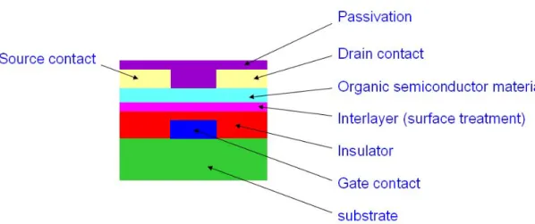
4 P e n t a c e n e t r a n s i s t o r s c a n b e u s e d a s a s w i t c h i n g d e v i c e f o r a c t i v e - m a t r i x d i s p l a y. T h e p e n t a c e n e f i l m s a r e u s u a l l y p o l y c r y s t a l l i n e w h e n t h e y a r e d e p o s i t e d b y o r g a n i c v a p o r p h a s e d e p o s i t i o n a n d t h e r m a l e v a p o r a t i o n . O t h e r a l s o h a v e s o m e s m a l l m o l e c u l a r s e m i c o n d u c t o r o r g a n i c m a t e r i a l s , s u c h a s L i n e a r f u s e d r i n g c o m p o u n d s , 2 - D f u s e d r i n g c o m p o u n d s , o l i g o m e r s a n d 3 - D m o l e c u l e s a n d s o o n . T h e p o l y m e r c o m p a r e s t o t h e s m a l l m o l e c u l a r h a s t h e h i g h e r m a n u f a c t u r e p r o c e s s s u p e r i o r i t y, B e c a u s e o f t h e o r g a n i c p o l y m e r m a n u f a c t u r e p r o c e s s c a n a p p l y t h e t e c h n o l o g y o f s o l u t i o n c o a t i n g . S u c h a s s p i n - c o a t i n g , d i p - c o a t i n g a n d p r i n t i n g p r o c e s s a n d s o o n . C o n s e q u e n t l y, m a n u f a c t u r e p r o c e s s m o r e i s e a s y t o a p p l y i n o n t h e l a r g e a r e a d e v i c e . R e g i o r e g u l a r P o l y ( 3 - a l k y l t h i o p h e n e ) ( P 3 H T ) i s P - t y p e o f t h e o r g a n i c p o l y m e r m o s t h a s t h e t y p i c a l m a t e r i a l . Vi e w f i g u r e 1 - 5 . A t p r e s e n t m a y u t i l i z e o n t h e p h o t o e l e c t r i c d e v i c e , a n d t h e t r a n s i s t o r h a s s u p e r i o r c h a r a c t e r i s t i c o f m o b i l i t y. P o l y ( b e n z o b i s i m i d a z o b e n z o p h e n a n t h r o l i n e ) ( B B L ) i s N - t y p e o f t h e o r g a n i c p o l y m e r m o s t h a s t h e t y p i c a l m a t e r i a l . H e r e i n t o , P o l y ( 9 , 9 - d i o c t y l f l u o r e n e c o - b i t h i o p h e n e ) ( F 8 T 2 ) i s o n e k i n d m a t e r i a l o f T h e r m o t r o p i c l i q u i d c r y s t a l . I t m a y a p p l y i n p r i n t i n g p r o c e s s a c h i e v - e d l a r g e l y r e d u c e s t h e p r o d u c t i o n c o s t . T h e c o m p l e x m o s t h a v e t h e t y p i c a l m a t e r i a l s s u c h a s P h t h a l o c - y a n i n e C o o r d i n a t i o n C o m p o u n d a n d O r g a n i c - i n o r g a n i c H y b r i d M a t e r i a l . M o r e o v e r P h t h a l o c y a n i n e C o o r d i n a t i o n C o m p o u n d i s m o s t e a r l y a p p l i e d o n t h e s e m i c o n d u c t o r i n g o r g a n i c d e v i c e .
Organic thin-film transistors (OTFT) based on conjugated polymers, oligomers, or other molecules have been envisioned as a viable alternative to more traditional, mainstream thin-film transistors (TFT) based on inorganic materials. Because of the relatively low mobility of the organic semiconductor layers, OTFT can’t rival the performance of field-effect transistors based on single-crystalline inorganic semiconductors, such as Si, Ge, GaAs, InP, which have charge carrier mobilities about three orders of magnitude higher [21].
5
1 . 2 . 2 S o u r c e / D r a i n c o n t a c t
T h e p o s i t i o n o f t h e F e r m i l e v e l i s a q u i t e i m p o r t a n t c o n s i d e r a t i o n i n t h e s e m i c o n d u c t o r. A s a r e s u l t o f m e t a l l i c w o r k f u n c t i o n c o n s i d e r - a t i o n , w h e t h e r f o r m s b a r r i e r o r o h m i c c o n t a c t i n t e r f a c e b e t w e e n m e t - a l a n d s e m i c o n d u c t o r. a n d i t i s d e c i d e d t o t h e f e r m i l e v e l p o s i t i o n . T h e r e w i t h j u d g e s f e r m i l e v e l t h e r e l a t i v e p o s i t i o n t o d e c i d e t y p e o f c o n d u c t i o n c o n d i t i o n . I f s e m i c o n d u c t o r f e r m i l e v e l a p p r o a c h e s v a l e - n c e b a n d , t r e a t s a s b y t h e h o l e c a r r i e s t o c o n v e y. T h e r e f o r e i s c a l l e d t h e p - t y p e s e m i c o n d u c t o r. A d v e r s a t i v e , i f s e m i c o n d u c t o r f e r m i l e v e l a p p r o a c h e s c o n d u c t i o n b a n d , t r e a t s a s b y t h e e l e c t r o n c a r r i e s t o c o n v e y. T h e r e f o r e i s c a l l e d t h e n - t y p e s e m i c o n d u c t o r. C o n s e q u e n t l y, w e w i l l i m p r o v e i n t e r f a c e t o a v o i d f o r m i n g S c h o t t k y b a r r i e r a n d c r e a t e s o v e r s i z e d c o n t a c t r e s i s t a n c e t o a f f e c t t h e d e v i c e c h a r a c t e r i s t - i c s . 1 . 2 . 3 H i g h d i e l e c t r i c c o n s t a n t i n s u l a t o rIn recent years, the organic thin film transistor (OTFT) has been studied widely on flexible electronic circuit for the application such as e-books, e-papers, and RF tags [1-3]. The effect of flexible electronic products for human life will grow drastically in the near future. A reliable low temperature process becomes more and more important and urgent for OTFT fabrication since a critical issue in OTFT fabrication is that the flexible substrate cannot suffer high temperature. There are some low temperature methods used to fabricate inorganic gate insulator reported in many studies such like sputter, electron-gun, and anodic oxidation [4-6]. Although the dielectric could be deposited or grown at low temperature, however, in order to reduce gate leakage current for obtaining a good gate dielectric property, a high temperature annealing after dielectric deposited is needed. Besides, a good gate insulator with high dielectric constant at low-temperature process is urgently demanded for the portable application on OTFT now. A low operation voltage for OTFT is required to reduce power consumption from flexible electronic circuits. By adopting some
6
high dielectric constant materials such as Al2O3[8], TiO2[7], HfO2[6] and TaO2[5] for
OTFT are a common way to reduce the operation voltage. Increase dielectric constant with reduce leakage current for OTFT, phenomenon of leakage current involve defect density and charge trap density at low temperature process,
charge trapped in defects causes a shift in the gate threshold voltage of the OTFT, the trapped charge will change with change with time so the threshold voltage will shift with time, leading to instability of operating characteristics, and occur increase scatter carriers so that low mobility for OTFT performance, hence, influence of dielectric quality is important for OTFT research.
1 . 2 . 4 A c t i v e r e g i o n p a t t e r n
I n o r d e r t o o b t a i n s t h e h i g h e f f i c i e n c y t h e e x p e r i m e n t , d e v e l o p s m a n y c o n v e n i e n c e s p r o c e s s t e c h n o l o g y, a v a r i e t y o f s t r a t e g i e s h a v e b e e n u s e d t o c r e a t e i n t e g r a t e d a r r a y s o f t r a n s i s t o r s i n c l u d i n g p h o t o l i t h o g r a p h y, s t a m p i n g , a n d s h a d o w m a s k i n g , p h o t o l i t h o g r a p h y h a s a n e s t a b l i s h e d i n f r a s t r u c t u r e t h a n k s t o i t s e x t e n s i v e u s e i n s i l i c o n f a b r i c a t i o n , p r i n t i n g p r o c e s s i n w h i c h t h e p r i n t i n g s u r f a c e i s n e i t h e r r a i s e d n o r e t c h e d i n t o t h e p l a t e , a n d p r i n t i n g i s a f f e c t e d b y m e a n s o f a c h e m i c a l p r o c e s s t h a t a l l o w s i n k t o a d h e r e t o o n l y t h e p a r t s o f t h e s u r f a c e t o b e r e p r o d u c e d . P h o t o l i t h o g r a p h i c p a t t e r n i n g h a s s e v e r a l a d v a n t a g e s : a r b i t r a r y p a t t e r n s c a n b e u s e d w i t h f i n e f e a t u r e s , a v a r i e t y o f d e p o s i t i o n t e c h n i q u e s m a y b e u s e d , a n d p h o t o l i t h o g r a p h y c a n b e a p p l i e d o v e r l a r g e a r e a s i n m u l t i l a y e r p r o c e s s .1 . 2 . 5 P a s s i v a t i o n
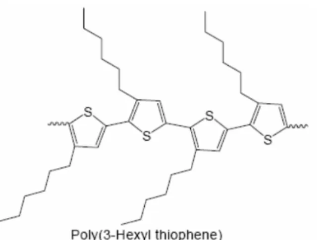
The degradation of electrical characteristics was observed, show figure 1-7. It is supposed, the reason is sheer stress by the viscosity of PVA when it was coated and dried. Because of the reason, we developed a novel encapsulation method for OTFTs. OTFTs were packaged by novel encapsulation method; the Al film adhered onto the pentacene
7
active layer in a dry nitrogen atmosphere using a proper adhesive. Using this method, we observed no degradation, view figure 1-8. No substantial degeneration occurred. The initial mobility of no passivation device the characterization was degraded after long terms. Their mobility is reduced to 2% of initial mobility value. Hence, a lifetime was defined as the time necessary to reduce mobility to 2% of initial mobility value. Through this result, the performance and the stability were observed by the novel encapsulation effect[15].
1 . 2 . 6 S u r f a c e t re a t m e n t
T h e d i e l e c t r i c p o l a r i t y i s m o d i f i e d b y t h e s e l f - a s s e m b l e d m o n o l a y e r ( S A M ) o n i n o r g a n i c d i e l e c t r i c s . I n o r g a n i c d i e l e c t r i c s w i t h l o w e r s u r f a c e e n e r g y p r o f f e r i m p r o v e d d e v i c e p e r f o r m a n c e ; s u c h s u r f a c e s r e d u c e m a n y o f i n t e r f a c e t r a p s i n O T F Ts [ 9 , 1 0 ] . H o w e v e r, c o n t r o l l i n g g a t e l e a k a g e i s a n e x t r a d i f f i c u l t y [ 1 1 ] . A s w e l l a s t h e i n c r e a s e i n c a p a c i t a n c e , t h e s u r f a c e p o l a r i t y ( h y d r o p h i l i c o r h y d r o p h o b i c ) o f t h e g a t e d i e l e c t r i c i s a n i m p o r t a n t f a c t o r [ 5 ] . H o w e v e r, t h e i n o r g a n i c m e t a l o x i d e d i e l e c t r i c w i t h h i g h e r p o l a r i z a b i l i t y l e a d s t o t h e h i g h e r O - H g r o u p d e n s i t y o n t h e i n t e r f a c e a n d o p p o s i t e l y r o u g h s u r f a c e m o r p h o l o g y. T h e f o r m e d O - H g r o u p s a n d t h e r o u g h s u r f a c e f u r t h e r a f f e c t i o n t h e u n p r o f i t a b l e q u a l i t y o f d e v i c e p e r f o r m a n c e s . B y t h i s r e a s o n , t h e p o l y m e r - c o a t i n g m a n n e r a p p e a r s t o b e a b s o l u t e l y p e r v a s i v e a n d t h u s c o u l d b e u s e d t o a n y d i e l e c t r i c s u r f a c e b e f o r e o r g a n i c s e m i c o n d u c t o r d e p o s i t i o n [ 1 2 - 1 4 ] . I n o r d e r t o s u c c e s s f u l l y i n t e g r a t e w i t h O T F Ts t e c h n o l o g y, t h e r e a r e a f e w i m p o r t a n t i s s u e s t o b e a d d r e s s e d , i n c l u d i n g d e g r a d a t i o n i n c h a n n e l m o b i l i t y, c h a r g e t r a p p i n g , a n d t h e r m a l s t a b i l i t y.1 . 2 . 7 D e v i c e s t r u c t u r e
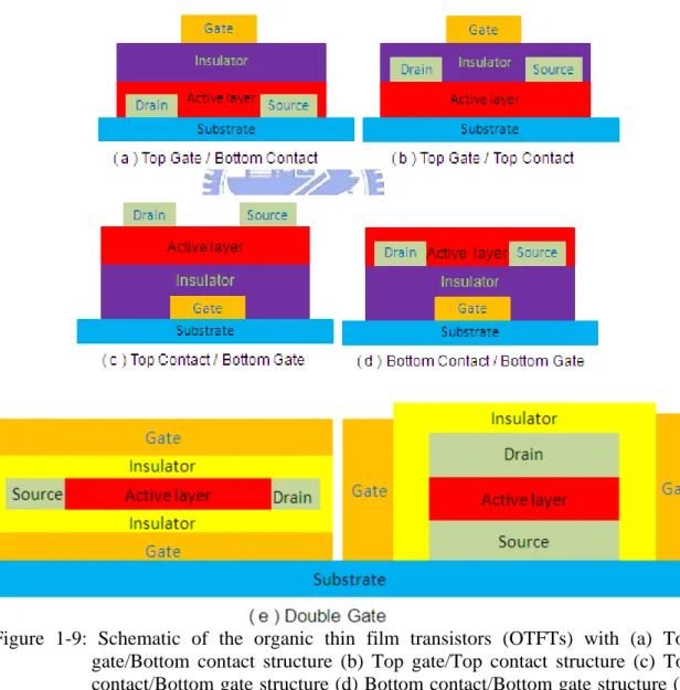
U s u a l l y, t e s t s t r u c t u r e s o f O T F T a r e u s u a l l y f a b r i c a t e d i n s h o w n f i g u r e 1 - 9 . To p g a t e a d v a n t a g e s w e r e s l e f - p a s s i v a t i o n a n d f i n e s o u r c e8
/ d r a i n r e s o l u t i o n , b u t d i s a d v a n t a g e s w e r e p o o r s e m i c o n d u c t o r / d i e l e c - t r i c i n t e r f a c e a n d h i g h c o n t a c t r e s i s t a n c e .
1.3 Gate dielectric for organic and inorganic materials
Organic dielectrics can be solution-processed, provide smooth films on transparent glass and plastic substrates, are suitable for optic-electronics like photo-responsive OFETs
due to their high optical transparency, can be thermally stable up to 200℃ with a relatively
small thermal expansion coefficient, and can posses a rather high dielectric constant up to 18.
Required properties for gate dielectrics.
1. Good for pentacene growth (for high mobility).
2. Should have low leakage current (for high on/off ratio). 3. Good chemical resistance (for high resolution).
4. Spin on material (for low cost). 5. High k (for low power).
9
1.4 Introduction of APPT
The atmospheric-pressure plasma technology (APPT) is useful for treating and modifying the surface properties of organic and inorganic materials. The APPT apparatus does not require any vacuum systems, produces high density plasma, and provides treatment of various substrates at low temperatures while operating open to the atmosphere. The plasma system has used for a wide variety of applications including treatment of polymer films, paper, wood, and foils; plasma grafting and plasma polymerization; ash various materials in the microelectronics industry; barrier layer deposition for the packaging industry; and sterilizing biologically contaminated materials.
For polymer films, the technique offers the following advantages:
• Uniform treatment and No backside treatment.
• Improved surface energy with concomitant improved wet ability, printability, and adhesion.
• No additional vacuum system and low cost.
• Continuous fabrication availably and high speed for production.
• High plasma density.
As shown in Fig.1-10, we exhibited the atmospheric-pressure plasma system which was used in our experiment.
From the viewpoint of processes, deposition method of SAPPT is more efficient than that of E-gun for the OTFT process since SAPPT does not need a vacuum system. This takes advantages of reduced process time and cost of the equipment. The electric properties of OTFT device fabricated at low temperature processes are demonstrated.
10
1-5 Thesis Organization
In this study, properties of silicon oxide deposited by SAPPT and E-gun system on silicon substrate are discussed. In addition, a suitable condition for silicon oxide deposited by SAPPT was selected from different temperature biases using MIS and MIM test structures.
In chapter 1, we describe application and Motivation of Organic Thin Film Transistor. Than acquaint with issues for fabrication OTFT structures, and technique of APPT.
In chapter 2, we adopt a new process, APPT, which can be operated under low temperature and atmospheric ambient. And APPT will make use of dielectric layer SiO2
for our experiment. We use to two different systems deposited silicon oxide as insulator dielectric layer which to test insulator quality of handicapper convenient for metal insulator semiconductor ( MIS ), metal insulator metal ( MIM ) and amorphous silicon metal insulator metal ( a-Si MIM ) structures.
In chapter 3, we use different structures to experiment with silicon oxide dielectric layer quality and leakage current.
11 R e f : W i l l i a m A . M a c D o n a l d “ A d v a n c e d F l e x i b l e P o l y m e r S u b s t r a t e s ” p . 1 6 5 F i g u r e 1 - 1 : C o m p a r e w i t h temperature f o r a v a r i e t y o f f l e x i b l e e l e c t r o n i c s u b s t r a t e s . R e f : M R S 2 0 0 2 F l e x I C s Ta b l e 1 - 1 : C o m p a r e w i t h characterization f o r a v a r i e t y o f f l e x i b l e e l e c t r o n i c s u b s t r a t e s .
12
Figure 1-2: Construction of o r g a n i c t h i n - f i l m t r a n s i s t o r
13
Figure 1-3: Classification of semiconductor materials
Figure 1-4: Molecular structure of pentacene.
14
R e f : Synthetic Metals 143 (2004) 21–23
Figure 1-6: Influence of mobility for OTFT passivation.
R e f : Current Applied Physics 5 (2005) 348–350
Figure 1-7: The electrical characteristics of OTFT encapsulated by the PVA coating method.
R e f : Current Applied Physics 5 (2005) 348–350 Figure 1-8: The electrical characteristics of OTFT encapsulated by polyacrylate-based
15
Ref: Organic electronics 8 (2007) 450-454.
Table 1-3: Characterization of contact angle for organic and inorganic materials
Figure 1-9: Schematic of the organic thin film transistors (OTFTs) with (a) Top gate/Bottom contact structure (b) Top gate/Top contact structure (c) Top contact/Bottom gate structure (d) Bottom contact/Bottom gate structure (e) Double gate structures.
16
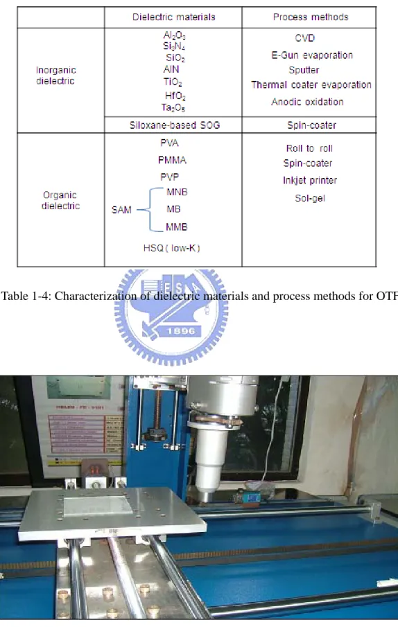
Table 1-4: Characterization of dielectric materials and process methods for OTFT
17
Chapter 2
Experiment
2.1 Silicon oxide deposited with E-gun and SAPPT equipments on the
metal insulator semiconductor ( MIS ) structure
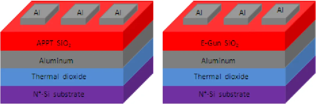
In this scenario, we use to two different systems deposited silicon oxide as insulator dielectric layer which to test insulator quality of handicapper convenient for metal insulator semiconductor ( MIS ) structure.
First, the n+-Si wafer was used as the substrate, and was rinsed in the deionization water ( DI water ), and was then dipped in dilute HF solution ( HF:DI water = 1:100 ) that to remove the native oxide, the wafer was accomplished the RCA Clean procedure after, deposition of silicon oxide were electron-beam ( e-gun ) technique and atmospheric-pressure plasma technology ( APPT ), respectively.
In atmospheric-pressure plasma technology aspect, Heats up the Tetraethoxy silane ( TEOS ) to 180℃ was injected by nitrogen ( 50% ) and oxygen ( 50% ) as carrier gases which was the deposition source of silicon oxide. The plasma power was established around 50 W with an appropriate scanning rate ( sccm /cycle ) to deposit silicon oxide on the top of n+-Si substrate at room temperature under an atmospheric- pressure. The thickness of silicon oxide was increased with the scanning times ( cycle/area ) , and we adopted 80 times and flow 1 sccm parameters to compare with different silicon oxide dielectrics.
In electron-beam technique aspect, the silicon substrate was deposited 60 nm thick remained at room temperature ( 25℃ ) that the deposition rate and vacuum pressure were 0.05 nm/sec and 4×10⁻⁶ Torr, respectively. Finally, all top contact electrodes were deposited 300 nm thick aluminum layer defined with shadow mask by thermal coater system. The active region pad of all capacitors was diameter 200 µm and all bottom contact electrode were deposited 300 nm thick aluminum layer before the bottom n+-Si substrate swabs the sponge of dilute HF solution.
2.2 Silicon oxide deposited with effect of substrate temperature by
SAPPT on the metal insulator metal ( MIM ) structure
18
In this scenario, we purpose to deposit silicon oxide dielectric on the bottom contact electrode metal by atmospheric-pressure plasma technology. But silicon oxide was not deposited on the metal at room temperature. Consequently, we try to find solution to heat up to the n+-Si substrate that was able to deposit on the metal.
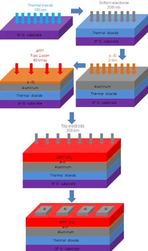
First, the n+-Si wafer was used as the substrate, and was rinsed in the deionization water ( DI water ), and was then dipped in dilute HF solution ( HF:DI water = 1:100 ) that to remove the native oxide, the wafer was accomplished the RCA Clean procedure after, deposition of silicon dioxide was thermal kiln grown 500 nm thick on the top of n+-Si substrate for isolation purpose. And deposited 300 nm aluminum as the bottom electrode. Heats up the Tetraethoxy silane ( TEOS ) to 180℃ was injected by nitrogen ( 50% ) and oxygen ( 50% ) as carrier gases which was the deposition source of silicon oxide. The plasma power was established around 50 W with an appropriate scanning rate ( sccm /cycle ) to deposit silicon oxide on the top of n+-Si substrate at room temperature under an atmospheric-pressure. The thickness of silicon oxide was increased with the scanning times ( cycle/area ) , silicon oxide was deposited on the aluminum thin film by atmospheric-pressure plasma technology ( APPT ) with varied substrate temperature (was treated at 100℃ , 150℃, and 200℃ respectively). Than we adopted 60 times and flow 1 sccm parameters to compare with different silicon oxide dielectrics.
Finally, all top contact electrode were deposited 300 nm thick aluminum layer defined with shadow mask by thermal coater system. The active region pad of all capacitors was diameter 200 µm .
2.3 Deposition of silicon oxide dielectric under room temperature on
amorphous silicon metal insulator metal ( a-Si MIM ) structure
In this scenario, we purpose to deposit silicon oxide dielectric on the bottom contact electrode metal by atmospheric-pressure plasma technology. But silicon oxide was not deposited on the metal at room temperature. Consequently, we try to find solution to deposit amorphous silicon on the bottom electrode metal by electron-beam technique that was able to deposit on the metal at room temperature.
First, the n+-Si wafer was used as the substrate, and was rinsed in the deionization water ( DI water ), and was then dipped in dilute HF solution ( HF:DI water = 1:100 )
19
that to remove the native oxide, the wafer was accomplished the RCA Clean procedure after, deposition of silicon dioxide was thermal kiln grown 500 nm thick on the top of n+-Si substrate for isolation purpose. And deposited 300 nm aluminum as the bottom electrode.
Then, we deposited amorphous silicon thickness of 2 nm by electron-beam technique that in order to easeful grow silicon oxide by atmospheric-pressure plasma technology at room temperature.
Heats up the Tetraethoxy silane ( TEOS ) to 180℃ wae injected by nitrogen ( 50 % ) and oxygen ( 50% ) as carrier gases which was the deposition source of silicon oxide. The plasma power was established around 50 W with an appropriate scanning rate ( sccm /cycle ) to deposit silicon oxide on the top of n+-Si substrate at room temperature under an atmospheric-pressure. The thickness of silicon oxide was increased with the scanning times ( cycle/area ) , silicon oxide was deposited on the aluminum thin film by atmospheric-pressure plasma technology ( APPT ) with varied scanning times ( at 60, 80, 100, and 120 times respectively). Than we adopted flow 1 sccm parameter to compare with different silicon oxide dielectrics.
Finally, all top contact electrode were deposited 300 nm thick aluminum layer defined with shadow mask by thermal coater system. The active region pad of all capacitors was diameter 200 µm .
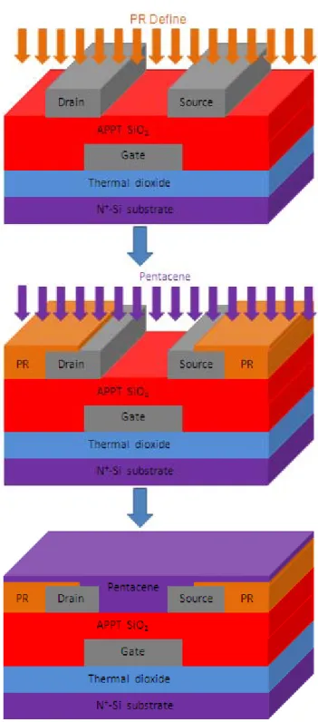
2.4 Fabricated processes of organic thin film transistor ( OTFT )
In this scenario, we adopted flow 1 sccm and 60 times parameters to deposit insulator as gate dielectric layer on the organic thin film transistor structure by atmospheric-pressure plasma technology ( APPT ).
First, the n+-Si wafer was used as the substrate, and was rinsed in the deionization water ( DI water ), and was then dipped in dilute HF solution ( HF:DI water = 1:100 ) that to remove the native oxide, the wafer was accomplished the RCA Clean procedure after, deposition of silicon dioxide was thermal kiln grown 500 nm thick on the top of n+-Si substrate for isolation purpose. The bottom contact structure was adopted to fabricate organic thin film transistor. That the structure of organic thin-film transistor. And deposited 50 nm thick aluminum layer as the gate electrode by lift-off method. The aluminum layer was deposited by thermal coater and silicon oxide deposited by
20
atmospheric-pressure plasma technology ( APPT ) at 150℃ under an atmospheric pressure with scanning 60 times was used as gate insulator. Source/ Drain electrodes with 50 nm thick nickel layer were deposited by electron-beam technique. The active layer used in this study was pentacene (obtained from Aldrich Co., Ltd.) which was evaporated by thermal coater. During deposition of pentacene active layer, the substrate was heated to 70℃ at power 17 W in a pressure chamber of around 1x10⁻⁶ Torr.
2.5 Characteristic measurement of devices
Capacitance-Voltage (C-V) characteristic diagrams were analyzed at 1MHz by HP 4284A precision LCR meter parameter and the characteristic curves of Current-Voltage (I-V) were measured with semiconductor parameter analyzer by HP 4156. All measurements were carried out at room temperature in an air atmosphere.
21
23
24
26
27
Chapter 3
Results and Discussion
3.1 Silicon oxide dielectric layer quality analysis and appraisal
3.1.1 MIS
We use to two different systems deposited silicon oxide as insulator dielectric layer which to test insulator quality of handicapper convenient for metal insulator semiconductor ( MIS ) structure. Sample A and sample B was APPT and E-Gun deposition respectively.
The C-V characterization of sample A and sample B was shown in Figure 3-1. EOT (Equivalent Oxide Thickness) calculated from capacitance of Figure 3-1(a) for sample A and sample B was about 8.277 nm and 10.919 nm respectively. The expression of EOT is very popular for the high dielectric constant gate insulator of CMOS device [16]. Because there are many kinds of insulator materials with different dielectric constants, EOT could be considered as a standard for a comparison of the gate insulator controllability to channel accumulation. The calculation of EOT is presented at equation ( 3-1 ). The circular area of top electrode in this study was diameter 200 µm .
( 3-1 )
The relationship between I-V of sample A and sample B were showed in Figure 3-1(b). The leakage current of sample B is higher than sample A at 1.5V bias voltage. However, because we want to know the effect of silicon oxide deposited by e-gun and SAPPT at different physical thickness, we try to make the comparison under the same electric field obtained from the voltage divided by the EOT (EEOT= Bias Voltage / EOT).
When two OTFT devices are biased at the same EEOT, which means the same
charges were accumulated at both device’s channels. In this case, when the EEOT was 1.5
MV/cm, leakage current of sample B is higher than sample A. Show figure 3-1 (c ).
28
3.1.2 MIM
We purpose to deposit silicon oxide dielectric on the bottom contact electrode metal by atmospheric-pressure plasma technology. But silicon oxide was not deposited on the metal at room temperature. Consequently, we try to find solution to heat up to the n+-Si substrate that was able to deposit on the metal. Silicon oxide of sample D ~ F was deposited by SAPPT on the bottom electrode surface at different substrate temperature at 100℃, 150℃, and 200℃. The horizontal axis and vertical axis of Figure 3-2 represent the swept voltage set and the value of capacitance respectively. The values of EOT calculated from Figure 3-2 (a) of sample D, E, and F were about 20.198 nm, 23.836 nm, and 28.496 nm respectively, so we could find that the deposition rate was increased with the substrate temperature. However, the capacitance value of sample C couldn’t be measured due to the high leakage current. The I-V characterization of sample C shows almost short circuit current, which implies the deposition rate was almost zero when we deposited silicon oxide on the surface of aluminum at room temperature. This situation is very different to that by deposited on silicon substrate at room temperature. These results revealed that the surface material is a main factor for SAPPT method to deposit silicon oxide at room temperature. The leakage current density versus electric field was shown in Figure 3-3. The leakage current of sample E and sample E-Gun is about 9×10⁻⁸ A/cm2and 2×10⁻⁷ A/cm2at 0.5 MV/cm respectively. The quality of silicon oxide deposited by SAPPT at 150℃ is better than that deposited by e-gun.
3.1.3 a-Si MIM
We purpose to deposit silicon oxide dielectric on the bottom contact electrode metal by atmospheric-pressure plasma technology. But silicon oxide was not deposited on the metal at room temperature. Consequently, we try to find solution to deposit amorphous silicon on the bottom electrode metal by electron-beam technique that was able to deposit on the metal at room temperature. Silicon oxide was deposited on the aluminum thin film by atmospheric-pressure plasma technology ( APPT ) with varied scanning times at 60, 80, 100, and 120 times respectively. Than we adopted flow 1 sccm parameter to compare with different silicon oxide dielectrics.
The horizontal axis and vertical axis of Figure3-4 represent the swept voltage set and the value of capacitance respectively. The values of EOT calculated from Figure3-4
29
(a) of sample 60, 80, 100, and 120 times were about 18.072 nm, 19.715 nm, 24.643 nm and 27.108 nm respectively,
The leakage current density versus electric field was shown in Figure 3-5. The leakage current of sample E-Gun is about 2×10⁻⁷ A/cm2 at 0.5 MV/cm respectively. The quality of silicon oxide deposited by e-gun is better than that deposited by SAPPT.
3.2 Determination of Threshold voltage and Mobility
The linear regime field effect mobility can be obtained by the calculation described below. At low VD, ID increases linearly with VD (linear regime) and is
approximately determined by the following equation:
(
)
[
G T D D]
ox n D V V V V L C W I 2 2 2 + − = µ( 3-2 )
where L is the channel length, W is the channel width, Cox is the capacitance per unit
area of the insulating layer, VT is the threshold voltage, and µ is the field effect mobility,
which can be calculated in the linear regime from the transconductance,
G
m = nCoxVD L Z µ = ∂ ∂ G D V I( 3-3 )
by plotting ID versus VG at a constant low VD, with –VD <<-(VG - VT), and equating the
value of the slope of this plot to Gm, then find Gmmax which can gain the value of
threshold voltage (VT) and linear mobility. For the known values included Cox, VT, and
W/L, the value of saturation mobility can be obtained from equation (3-4)
(
)
2 2 ) ( n ox G T D V V L C W sat I =µ
+( 3-4 )
3.3 OTFT electric characteristics analysis and discussion
At this part, SAPPT method was adopted to fabricate the gate insulator of OTFT with the parameters of sample E discussed. Process temperature and throughput are the two main considerations for this selection. First, most plastic substrates could not sustain temperature higher than 200℃. The process condition of sample E (150℃) provides a suitable thermal buffer for flexible electronic device fabrication. Secondly, the deposition rate is increased with the raised process temperature and the condition of sample E has a relatively higher deposition rate than sample D. The condition of sample
30
E is still a low temperature process and can get a better deposition rate for throughput and still maintain good quality. The drain current (ID) versus drain-source voltage (VDS)
at varied gate voltages (VGS) was shown in Figure 3-8(a). The output characteristic of ID
versus VGSwas shown in Figure 3-8(b). The carrier mobility was calculated at the
saturation region with following equation:
( 3-5 )
Ci is the capacitance per unit area of gate insulator in equation. (3-5). It correspond to a device with channel width W = 200 µm and length L = 50 µm. The saturation mobility and the threshold voltage of the OTFT were about 0.066 cm2/V-sand - 2 V respectively. The OTFT could be operated at the voltage below -5 V due to the EOT of about 14 nm. However, the mobility of this device was lower than some other reports [17, 18]. We suggested that three possible reasons could explain this phenomenon. First, since we fabricated the OTFT device with bottom contact structure [2], the grain size of the active layer would be affected by the roughness of the electrodes of source and drain. Secondly, the roughness of aluminum gate electrode was about 8.7 nm (the corresponding AFM analysis was shown in Figure 3-14(a)), the roughness of the silicon oxide deposited by SAPPT on the top of aluminum gate electrode was around 10.8 nm (see Figure 3-14(b)). Third, the contact angle of gate insulator with DI water was about 20 degree and figure 3-15 shows hydrophilic characteristic at the surface of the silicon oxide. Roughness and hydrophilic characteristic might be the main factors to influence the deposition of pentacene and then decrease the mobility of OTFT devices. [18-20].
3.4 Leakage current characteristic of OTFT discussion in various
structures
We can see leakage current 3×10⁻⁷ A at drain/source voltage and gate voltage was zero and -7 respectively. In figure 3-8(b). Consequently, we to discuss for leakage current in the different structure. View from figure 3-9 to figure 3-13.
First, we compare with define pentacene region and not define pentacene region in figure 3-9. Result in leakage current of not define pentacene region is higher than define pentacene region. Because of not define pentacene region have large field that account to more leakage current. And we adopt two materials to experiment, we obtain the same result. Hence, define pentacene region is important for OTFT divice that can be
31
effective reduce leakage current.
We compare with have HMDS and not have HMDS in figure 3-11. Result in leakage current of have HMDS is higher than not have HMDS. Because of HMDS can be increase pentacene grain size and increase pentacene conductivity. Therefore, we found have HMDS not only the increase conductive merit but also increases leakage the current shortcoming. In figure 3-12 and figure 3-13, leakage current of not define pentacene region is higher than define pentacene region and leakage current of have pentacene is higher than not have pentacene.
32
Figure 3-1: The electronic characterization of MIS.
0.5 1.0 1.5 2.0 2.5 0.0 1.0x10⁻⁶ 2.0x10⁻⁶ 3.0x10⁻⁶ 4.0x10⁻⁶ 5.0x10⁻⁶ 6.0x10⁻⁶ 7.0x10⁻⁶ 8.0x10⁻⁶ 9.0x10⁻⁶ 1.0x10⁻⁵ 1.1x10⁻⁵ 1.2x10⁻⁵ 1.3x10⁻⁵ 1.4x10⁻⁵ 1.5x10⁻⁵ 1.6x10⁻⁵ 1.7x10⁻⁵ Leaka ge Current Den s ity ( A /cm 2 ) Bias ( V ) ( b ) MIS Flow 1 80 Times 8.277 nm E-Gun Evaporation 10.919 nm -2.0 -1.5 -1.0 -0.5 0.0 0.5 1.0 1.5 2.0 0.0 5.0x10⁻⁸ 1.0x10⁻⁷ 1.5x10⁻⁷ 2.0x10⁻⁷ 2.5x10⁻⁷ 3.0x10⁻⁷ 3.5x10⁻⁷ 4.0x10⁻⁷ 4.5x10⁻⁷ Ca paci ta n ce De nsity ( F /cm 2 ) Bias ( V ) (a) MIS Flow 1 80 Times 8.277 nm E-Gun Evaporation 10.919 nm 0.6 0.8 1.0 1.2 1.4 1.6 1.8 2.0 2.2 2.4 0.0 1.0x10⁻⁶ 2.0x10⁻⁶ 3.0x10⁻⁶ 4.0x10⁻⁶ 5.0x10⁻⁶ 6.0x10⁻⁶ 7.0x10⁻⁶ 8.0x10⁻⁶ 9.0x10⁻⁶ 1.0x10⁻⁵ 1.1x10⁻⁵ 1.2x10⁻⁵ 1.3x10⁻⁵ 1.4x10⁻⁵ 1.5x10⁻⁵ 1.6x10⁻⁵ 1.7x10⁻⁵ Lea kage Curr e n t Densi ty ( A/cm 2 ) V/EOT ( MV/cm ) ( c ) MIS Flow 1 80 Times 8.277 nm E-Gun Evaporation 10.919 nm
33
( a )
( b )
Figure 3-2: The electronic characterization of MIM for C-V and I-V.
-2.0 -1.5 -1.0 -0.5 0.0 0.5 1.0 1.5 2.0 8.0x10⁻⁸ 1.0x10⁻⁷ 1.2x10⁻⁷ 1.4x10⁻⁷ 1.6x10⁻⁷ 1.8x10⁻⁷ 2.0x10⁻⁷
MIM Flow 1 sccm 60 Times 100 0C 20.198 nm 150 0C 23.836 nm 200 0C 28.496 nm E-Gun Evaporation 16.183 nm Capacit ance Den s it y ( F /cm 2 ) Bias ( V ) 0.0 0.1 0.2 0.3 0.4 0.5 0.6 0.7 0.8 -9.0x10⁻⁸ -6.0x10⁻⁸ -3.0x10⁻⁸ 0.0 3.0x10⁻⁸ 6.0x10⁻⁸ 9.0x10⁻⁸ 1.2x10⁻⁷ 1.5x10⁻⁷ 1.8x10⁻⁷ 2.1x10⁻⁷ 2.4x10⁻⁷ 2.7x10⁻⁷ 3.0x10⁻⁷ 3.3x10⁻⁷
MIM Flow 1 sccm 60 Times 100 0C 20.198 nm 150 0C 23.836 nm 200 0C 28.496 nm E-Gun Evaporation 16.183 nm Cur rent Densit y ( A/ cm 2 ) Bias ( V )
34
( a )
( b )
Figure 3-3: The electronic characterization of MIM for I-V and I-E.
0.0 0.1 0.2 0.3 0.4 0.5 0.6 0.7 0.8 0.9 1.0 1.1 1.2 1.3 1.4 1.5 -1.0x10⁻⁷ 0.0 1.0x10⁻⁷ 2.0x10⁻⁷ 3.0x10⁻⁷ 4.0x10⁻⁷ 5.0x10⁻⁷
MIM Flow 1 sccm 60 Times 100 0C 20.198 nm 150 0C 23.836 nm 200 0C 28.496 nm E-Gun Evaporation 16.183 nm Cu rren t Den s it y ( A/ cm 2 ) Bias ( V ) 0.00 0.05 0.10 0.15 0.20 0.25 0.30 0.35 0.40 0.45 0.50 -1.2x10⁻⁷ -9.0x10⁻⁸ -6.0x10⁻⁸ -3.0x10⁻⁸ 0.0 3.0x10⁻⁸ 6.0x10⁻⁸ 9.0x10⁻⁸ 1.2x10⁻⁷ 1.5x10⁻⁷ 1.8x10⁻⁷ 2.1x10⁻⁷ 2.4x10⁻⁷ 2.7x10⁻⁷ 3.0x10⁻⁷ 3.3x10⁻⁷
MIM Flow 1 sccm 60 Times 100 0C 20.198 nm 150 0C 23.836 nm 200 0C 28.496 nm E-Gun Evaporation 16.183 nm Curr ent Dens it y ( A /c m 2 ) E ( MV/cm )
35
( a )
( b )
Figure 3-4: The electronic characterization of a-Si MIM for C-V and I-V.
0.0 0.2 0.4 0.6 0.8 1.0 1.2 1.4 1.6 1.8 2.0 1.2x10⁻⁷ 1.3x10⁻⁷ 1.3x10⁻⁷ 1.4x10⁻⁷ 1.4x10⁻⁷ 1.5x10⁻⁷ 1.5x10⁻⁷ 1.6x10⁻⁷ 1.6x10⁻⁷ 1.7x10⁻⁷ 1.7x10⁻⁷ 1.8x10⁻⁷ 1.8x10⁻⁷ 1.9x10⁻⁷ 1.9x10⁻⁷ 2.0x10⁻⁷ 2.0x10⁻⁷
a-Si MIM Flow 1 60 Times 80 Times 100 Times 120 Times E-Gun Evaporation Capa citance Den s ity ( F /cm 2 ) Bias ( V ) 0.0 0.1 0.2 0.3 0.4 0.5 0.6 0.7 0.8 0.9 1.0 1.1 1.2 1.3 1.4 1.5 -1.0x10⁻⁷ -5.0x10⁻⁸ 0.0 5.0x10⁻⁸ 1.0x10⁻⁷ 1.5x10⁻⁷ 2.0x10⁻⁷ 2.5x10⁻⁷ 3.0x10⁻⁷ 3.5x10⁻⁷ 4.0x10⁻⁷ 4.5x10⁻⁷ 5.0x10⁻⁷ 5.5x10⁻⁷ 6.0x10⁻⁷ 6.5x10⁻⁷ 7.0x10⁻⁷ 7.5x10⁻⁷ 8.0x10⁻⁷
a-Si MIM Flow 1 60 Times 18.072 nm 80 Times 19.715 nm 100 Times 24.643 nm 120 Times 27.108 nm E-Gun Evaporation Current Densi ty ( A/ cm 2 ) Bias ( V )
36
( a )
( b )
Figure 3-5: The electronic characterization of a-Si MIM for I-V and I-E. 0.0 0.1 0.2 0.3 0.4 0.5 0.6 0.7 0.8 0.9 1.0 1.1 1.2 1.3 1.4 1.5 -1.0x10⁻⁷ -5.0x10⁻⁸ 0.0 5.0x10⁻⁸ 1.0x10⁻⁷ 1.5x10⁻⁷ 2.0x10⁻⁷ 2.5x10⁻⁷ 3.0x10⁻⁷ 3.5x10⁻⁷ 4.0x10⁻⁷ 4.5x10⁻⁷ 5.0x10⁻⁷ 5.5x10⁻⁷ 6.0x10⁻⁷ 6.5x10⁻⁷ 7.0x10⁻⁷ 7.5x10⁻⁷ 8.0x10⁻⁷
a-Si MIM Flow 1 60 Times 18.072 nm 80 Times 19.715 nm 100 Times 24.643 nm 120 Times 27.108 nm E-Gun Evaporation Current Dens it y ( A/ c m 2 ) Bias ( V ) 0.0 0.1 0.2 0.3 0.4 0.5 0.6 0.7 0.8 0.9 0.0 5.0x10⁻⁸ 1.0x10⁻⁷ 1.5x10⁻⁷ 2.0x10⁻⁷ 2.5x10⁻⁷ 3.0x10⁻⁷ 3.5x10⁻⁷ 4.0x10⁻⁷ 4.5x10⁻⁷ 5.0x10⁻⁷ 5.5x10⁻⁷ 6.0x10⁻⁷ 6.5x10⁻⁷ 7.0x10⁻⁷ 7.5x10⁻⁷ 8.0x10⁻⁷ 8.5x10⁻⁷
a-Si MIM Flow 1 60 Times 18.072 nm 80 Times 19.715 nm 100 Times 24.643 nm 120 Times 27.108 nm E-Gun Evaporation Cur rent Dens it y ( A /cm 2 ) E ( MV/cm )
37
( a )
( b )
Figure 3-6: The electronic characterization of MIM, a-Si MIM and E-Gun for C-V and I-V. -2.0 -1.5 -1.0 -0.5 0.0 0.5 1.0 1.5 2.0 1.2x10⁻⁷ 1.3x10⁻⁷ 1.3x10⁻⁷ 1.4x10⁻⁷ 1.4x10⁻⁷ 1.5x10⁻⁷ 1.5x10⁻⁷ 1.6x10⁻⁷ 1.6x10⁻⁷ 1.7x10⁻⁷ 1.7x10⁻⁷ 1.8x10⁻⁷ 1.8x10⁻⁷ 1.9x10⁻⁷ 1.9x10⁻⁷ 2.0x10⁻⁷ 2.0x10⁻⁷ Flow 1 60 Times MIM 1500C a-Si MIM E-Gun Evaporation Cap a cit ance Density ( F /cm 2 ) Bias ( V ) 0.0 0.1 0.2 0.3 0.4 0.5 0.6 0.7 0.8 0.9 1.0 1.1 1.2 1.3 1.4 1.5 -1.0x10⁻⁷ -5.0x10⁻⁸ 0.0 5.0x10⁻⁸ 1.0x10⁻⁷ 1.5x10⁻⁷ 2.0x10⁻⁷ 2.5x10⁻⁷ 3.0x10⁻⁷ 3.5x10⁻⁷ 4.0x10⁻⁷ 4.5x10⁻⁷ 5.0x10⁻⁷ 5.5x10⁻⁷ 6.0x10⁻⁷ 6.5x10⁻⁷ 7.0x10⁻⁷ 7.5x10⁻⁷ 8.0x10⁻⁷ Flow 1 60 Times MIM 1500C a-Si MIM E-Gun Evaporation Curr ent Dens it y ( F /c m 2 ) Bias ( V )
38
( a )
( b )
Figure 3-7: The electronic characterization of MIM, a-Si MIM and E-Gun for I-V and I-E. 0.0 0.1 0.2 0.3 0.4 0.5 0.6 0.7 0.8 0.9 1.0 1.1 1.2 1.3 1.4 1.5 -1.0x10⁻⁷ -5.0x10⁻⁸ 0.0 5.0x10⁻⁸ 1.0x10⁻⁷ 1.5x10⁻⁷ 2.0x10⁻⁷ 2.5x10⁻⁷ 3.0x10⁻⁷ 3.5x10⁻⁷ 4.0x10⁻⁷ 4.5x10⁻⁷ 5.0x10⁻⁷ 5.5x10⁻⁷ 6.0x10⁻⁷ 6.5x10⁻⁷ 7.0x10⁻⁷ 7.5x10⁻⁷ 8.0x10⁻⁷ Flow 1 60 Times MIM 1500C a-Si MIM E-Gun Evaporation Curr ent Dens it y ( F /c m 2 ) Bias ( V ) 0.00 0.06 0.12 0.18 0.24 0.30 0.36 0.42 0.48 0.54 0.60 -1.0x10⁻⁷ -5.0x10⁻⁸ 0.0 5.0x10⁻⁸ 1.0x10⁻⁷ 1.5x10⁻⁷ 2.0x10⁻⁷ 2.5x10⁻⁷ 3.0x10⁻⁷ 3.5x10⁻⁷ 4.0x10⁻⁷ 4.5x10⁻⁷ 5.0x10⁻⁷ 5.5x10⁻⁷ 6.0x10⁻⁷
Flow 1 60 Times
MIM 150
0C
a-Si MIM
E-Gun Evaporation
Curr ent Dens it y ( F /c m 2 ) E ( MV/cm )39
( a )
( b )
Figure 3-8: The electronic characterization of OTFT for Id-Vg and Id-Vd.
-9 -8 -7 -6 -5 -4 -3 -2 -1 0 1 -1.4x10⁻⁶ -1.2x10⁻⁶ -1.0x10⁻⁶ -8.0x10⁻⁷ -6.0x10⁻⁷ -4.0x10⁻⁷ -2.0x10⁻⁷ 0.0 2.0x10⁻⁷ 4.0x10⁻⁷ Vg = 0 V Vg = -3 V Vg = -5 V Vg = -7 V I D ( A ) V DS ( V ) -5.0 -4.5 -4.0 -3.5 -3.0 -2.5 -2.0 -1.5 -1.0 -0.5 0.0 -1.0x10⁻⁸ 0.0 1.0x10⁻⁸ 2.0x10⁻⁸ 3.0x10⁻⁸ 4.0x10⁻⁸ 5.0x10⁻⁸ 6.0x10⁻⁸ 7.0x10⁻⁸ 8.0x10⁻⁸ 9.0x10⁻⁸ 1.0x10⁻⁷ 1.1x10⁻⁷ 1.2x10⁻⁷ 1.3x10⁻⁷ 1.4x10⁻⁷ 1.5x10⁻⁷ Vd = 0 V Vd = -3 V Vd = -5 V Vd = -7 V I D ( A ) V g ( V )
40
Figure 3-9: The electronic leakage current characterization of pentacene-HfO2 MIM for I-V. 0.0 0.1 0.2 0.3 0.4 0.5 0.6 0.7 0.8 0.9 1.0 1.1 1.2 1.3 1.4 1.5 -20.0p 0.0 20.0p 40.0p 60.0p 80.0p 100.0p 120.0p 140.0p 160.0p 180.0p 200.0p 220.0p 240.0p 260.0p 280.0p 300.0p 320.0p
HfO
2No Define
Define
Leakage Curr ent ( A ) Bias ( V )41
Figure 3-10: The electronic leakage current characterization of pentacene-SiO2 MIM for I-V. 0.0 0.1 0.2 0.3 0.4 0.5 0.6 0.7 0.8 0.9 1.0 1.1 1.2 1.3 1.4 1.5 0.0 1.0n 2.0n 3.0n 4.0n 5.0n 6.0n 7.0n 8.0n 9.0n 10.0n 11.0n 12.0n 13.0n
SiO
2No Define
Define
LeaKa ge Curren t ( A ) Bias ( V )42
Figure 3-11: The electronic leakage current characterization of pentacene-SiO2 MIM for I-V. 0.0 0.1 0.2 0.3 0.4 0.5 0.6 0.7 0.8 0.9 1.0 1.1 1.2 1.3 1.4 1.5 0.0 1.0n 2.0n 3.0n 4.0n 5.0n 6.0n 7.0n 8.0n 9.0n 10.0n 11.0n 12.0n 13.0n 14.0n
SiO
2Have HMDS
No HMDS
L e a k ag e Cu rre nt ( A ) Bias ( V )43
Figure 3-12: The electronic leakage current characterization of OTFT for HfO2.
0.0 0.1 0.2 0.3 0.4 0.5 0.6 0.7 0.8 0.9 1.0 0.0 20.0p 40.0p 60.0p 80.0p 100.0p 120.0p 140.0p 160.0p 180.0p 200.0p 220.0p 240.0p
HfO
2No PR Define
PR Define
No Pentacene
Leakage Current ( A ) Bias ( V )44
Figure 3-13: The electronic leakage current characterization of OTFT for SiO2.
0.0 0.1 0.2 0.3 0.4 0.5 0.6 0.7 0.8 0.9 1.0 0.0 20.0p 40.0p 60.0p 80.0p 100.0p 120.0p 140.0p 160.0p 180.0p 200.0p 220.0p 240.0p
SiO
2No PR Define
PR Define
No Pentacene
Leakage Current ( A ) Bias ( V )45
Figure 3-14:
( a ) shows the AFM image of aluminum gate insulator with roughness about 8.7 nm.
( b ) shows the AFM image silicon oxide deposited at 150℃ on the aluminum with the roughness around 10.8 nm.
46
Figure 3-15:
(a) shows the contact angle image silicon oxide deposited at 150℃ on the aluminum with the angle around 20°.
47
Chapter 4
Conclusion
4.1 Conclusion
From the experiment 3.1.1 and 3.1.2, we can know that the deposition rate of silicon oxide deposited by SAPPT at room temperature depend on the surface material where to deposit on. The leakage current of silicon oxide deposited by SAPPT at 150℃ (sample E) was about 9×10⁻⁸ A at 0.5 MV/cm which is around one order lower than that of the control sample G (E-gun deposition). Because sample E has better insulator property due to a higher deposition rate and suitable process temperature than other samples deposited by E-gun, its process condition was chosen to fabricate OTFT device. OTFT with the gate insulator deposited by scanning atmospheric-pressure technology was successfully demonstrated in experiment 3.1.3. The highest process temperature in the fabrication of OTFT device was 150℃. The operation voltage of this device is reduced to -5V due to the smaller EOT of 14 nm. Although the mobility of our device is lower than 0.1 cm2/V-s. The reasons for low mobility may be caused by the surface roughness of gate electrode and the hydrophilic surface in SAPPT process.
In summary, we already fabricated successfully OTFT with good dielectric property by using SAPPT method and demonstrated that SAPPT is a suitable method to fabricate good dielectric for the applications of plastic substrate due to the low temperature process under an atmospheric pressure.
48
4.2 Future work
• Improves the organic thin film transistor performance on surface treatment by atmospheric pressure plasma technology.
• Change gate electrode metal from aluminum to nickel , tellingly reduce surface roughness enhance organic thin film transistor performance .
• Because Pentacene OTFT are sensitive to ambient conditions. Protection from the environment by encapsulation is critical to the stability of Pentacene OTFT. Therefore, using a suitable material as passivation to protect Pentacene film from environmental effect is another important topic.
49
Reference
1. M. Shtein, J. Mapel, J. B. Benziger, and S. R. Forrest, Appl. Phys. Lett., 81 (2002) 268.
2. C.D. Dimitrakopoulos, D.J. Mascaro, IBM J. Res. Dev. 45 (1) (2001) 11. 3. F. M. Li, Y. Wu, and B. S. Ong, Appl. Phys. Lett., 90 (2007) 133514. 4. B. Carmen, J. Henri, and B. Staf, Organic Electronics 3 (2002) 65-72
5. Hsiao-Wen Zan, Kuo-Hsi Yen, Pu-Kuan Liu, Kuo-Hsin Ku, Chien-Hsun Chen, Jennchang Hwang Organic Electronics 8 (2007) 450–454.
6. J. Tardy, M. Erouel, A.L. Demanl, and V. Teodorescu, 2007 IEEE
7. J. B. Han, N. Wang, and Q. Q. Wang, Surface & Coating Technology 200 (2006) 4876-4878
8. J. Lee, J. H. Kim, and S. Im, J. Appl. Phys. 95 (2004) 3733
9. Kazumasa Nomoto, Nobukazu Hirai, Nobuhide Yoneya,Noriyuki Kawashima, Makoto Noda, Masaru Wada, Jiro Kasahara, IEEE Trans. Electron Dev. 52 (2005) 1519
10. Qing Cao, Zheng-Tao Zhu, Maxime G. Lemaitre, Ming-Gang Xia, Appl. Phys. Lett. 88 (2006) 113511.
11. Guangming Wang, Daniel Moses, Alan J. Heeger, Hong-Mei Zhang, Mux Narasimhan, R.E. Demaray, J. Appl. Phys.95 (2004) 316.
12. Jin Y, Rang Z, Nathan M I, Newman C R and Frisbie C D 2004 Appl. Phys. Lett. 85 4406.
13. Deman A L and Tardy J 2005 Org. Electron. 6 78.
14. Fritz S E, Kelley T W and Frisbie C D 2005 J. Phys. Chem. B 108 10574. 15. Current Applied Physics 5 (2005) 348–350.
16. D.A Buchanan, IBMJ. Res and Develop, vol.43, pp.245, 1999 17. F. C. Chen, C.W. Chu, and Y. Yang Appl. Phys. Lett., 85 (2004) 15
18. S. W. Cho, D. S. Park, W.C. Jang, and C-N Whang , Journal of Applied Physics 102 (2007).
19. H. Sirringhaus, P. J. Brown, R. H. Friend, M. M. Nielsen, K. Bechgaard, B. M. W. Langeveld-Voss, A. J. H. Spiering, R. A. J. Janssen, E. W. Meijer, P. Herwig, and D. M. de Leeuw, Nature, 401 (1999) 685
20. D. J. Gundlach, L. L. Jia, and T. N. Jackson, IEEE Electron Device Lett. 22 (2001) 571.
50
21. Y. Taur and T. H. Ning, Fundamentals of Modern VLSI Devices, Cambridge University Press, New York, (1998).