國 立 交 通 大 學
電 信 工 程 學 系 碩 士 班
碩 士 論 文
多媒體串列處理器之微架構模擬器
A Micro-architecture Simulator for Multimedia
Stream Processor
研究生:林芳如
指導教授:闕河鳴 博士
多媒體串列處理器之微架構模擬器
A Micro-architecture Simulator for Multimedia Stream Processor
研 究 生:林芳如
指導教授:闕河鳴 博士
Student:Fang-Ju Lin
Advisor:Dr. Herming Chiueh
國立交通大學
電信工程學系碩士班
碩士論文
A Thesis
Submitted to Institute of Communication Engineering College of Electrical Engineering and Computer Science
National Chiao Tung University in Partial Fulfillment of the Requirements
for the Degree of Master of Science in Communication Engineering January 2006 Hsinchu, Taiwan. 中華民國九十五年一月
多媒體串列處理器之微架構模擬器
學生:林芳如
指導教授:闕河鳴
國立交通大學電信工程學系碩士班
摘要
Stanford 針對多媒體應用程式發展出一個可程式化的處理器 Imagine。 由 於可程式化的 Stream Processor 針對不同的應用程式所適用的硬體架構會有所不 同,利用硬體實現各種不同的架構並且比較執行的效能,不但耗費很長的時間, 硬體製作的成本也非常的昂貴。 根據不同的多媒體應用程式,如何決定可程式 化 Stream Processor 的硬體架構,是一大難題。 然而現今的硬體加速電路,大 部分都是針對特定的用途而設計,其硬體架構的設計是針對特定的應用程式,才 能達到很好的執行效能。 在本論文中,將提出一個架構的模擬器,模擬多媒體 應用程式在不同架構上的執行效能,並分析硬體的使用率以及記憶體使用的容 量。 比較應用程式在各種架構上的執行效率,挑選出最適合的硬體架構。 決 定最佳化的硬體架構之後,可程式化的 Stream Processor 再用硬體去實現。 各 式各樣的多媒體應用程式,利用架構模擬器找出最佳化的硬體架構,再搭配可程 式化的 Stream Processor 將硬體實現,不但省下了硬體製作成本;速度相較於使 用硬體實現來測試也加快許多。A Micro-architecture Simulator for Multimedia
Stream Processor
Student: Fang-Ju Lin Advisor: Dr. Herming Chiueh
Institute of Communication Engineering National Chiao Tung University
Hsinchu, Taiwan 30050
Abstract
A programmable processor, Imagine, has been developed especially for media applications by Stanford. Since a programmable Stream Processor would build various hardware micro-architectures for diverse media applications, the cost of time and money could be huge to implement various micro-architectures on hardware and then compare their efficiencies. Therefore, how to construct suitable micro-architectures of programmable Stream Processor for diverse media applications is a great challenge. Nowadays, most of the hardware accelerators are designed for dedicated application. Only when the hardware micro-architecture is carefully designed for particular media application could the stream processor achieves exceptional performance. For the purpose of resolving this dilemma, in this paper, we develop the micro-architecture simulator for stream processor. The micro-architecture simulator is expected to simulate the performance of media application executed on various micro-architectures, and then to analyze the utility
rate of hardware and consumption of memory. By comparing the performance of media application executed on diverse micro-architectures, the optimized hardware micro-architecture can be determined and then the programmable Stream Processor can be implemented on hardware. By utilizing micro-architecture simulator to settle down optimized problems and then implement hardware with programmable Stream Processor for diverse applications, this idea saves not only huge cost of money on hardware, but also plenty of time for testing.
誌 謝
兩年的研究所生涯即將接近尾聲了,兩年的學習,讓我更加了解學海的無涯 知識的浩瀚。 首先我要感謝我的指導教授闕河鳴老師,以其豐厚的學術素養,在研究學問 的要領與態度給予啟發和指導,以及在學業及生活上給予協助與教導,讓我受益 良多。另外,也要感謝交大副校長黃威老師;清大電機系許雅三老師以及台大電 機系呂良鴻老師,百忙中撥冗擔任我的論文口試委員,對於我的論文給予建議, 著實獲益良多。 謝謝兩年來一起努力的實驗室成員們,謝謝他們對我的幫助及照顧。還要感 謝每天一起生活的室友們,在寫論文的過程中,互相打氣互相鼓勵,這本論文才 可以順利的完成。另外我要特別感激我的男朋友葉威廷,在研究所的兩年中,不 斷的給我鼓勵與動力,解開我課業上的疑惑,並且在我論文的撰寫過程中給予許 多的寶貴意見,以及幫我修改論文中文法的錯誤,從他身上學習到的,讓我有很 大的成長。 另外,還要感謝我最愛的兩隻狗寶貝,鬍子、達達,有了他們,讓我的生活 更加的多姿多采,永遠充滿歡笑。最後我要謝謝我的父母,哥哥,溫暖的家,永 遠都是我的避風港,不論面臨挫折或是困難,挑戰,都陪我一起度過,永遠都默 默的支持我。有了他們,我才可以順利拿到碩士的學位。Content
摘要...i
Abstract ...ii
誌 謝...iv
Content ...v
List of Figures ...vii
List of Tables...ix
Chapter 1 Introduction ...1
Chapter 2 Background ...5
2.1 Stream processing ...5
2.1.1 Stream programming model...6
2.1.2 Stream micro-architecture...8
2.1.3 An example of stream processor: Imagine...9
2.2 Current usage of micro-architecture simulator ...10
2.3 The importance of the micro-architecture simulator... 11
Chapter 3 Micro-architecture simulator...15
3.1 Organization of the micro-architecture simulator...16
3.2 Design methodology of the micro-architecture simulator ...17
3.2.1 Cluster ...17
3.2.2 ALU, MUL, DIV...19
3.2.3 Memory hierarchy...27
3.3 Mechanism of the micro-architecture simulator ...27
3.3.1 Parameter definition...28
3.3.3 Simulation ...30
3.4 Summary ...32
Chapter 4 Performance Evaluation ...33
4.1 Benchmark ...33
4.2 Experimental set-up ...34
4.2.1 Parameter definition...34
4.2.2 Translate FFT algorism into stream code...35
4.2.3 Data loading from main memory...36
4.3 Result of performance evaluation ...38
4.3.1 1-cluster stream micro-architecture simulation ...38
4.3.2 2-cluster stream micro-architecture simulation ...41
4.3.3 4-cluster stream micro-architecture simulation ...45
4.3.4 8-cluster stream micro-architecture simulation ...51
4.4 Performance comparison ...58
4.5 Summary ...61
Chapter 5 Conclusion and future work ...63
List of Figures
Figure 2.1 Stream and kernel representation………7
Figure 2.2 Stream processor block diagram………8
Figure 2.3 Contribution of the simulator…….………13
Figure 3.1 Simulation flow……….15
Figure 3.2 Block diagram of micro-architecture simulator………16
Figure 3.3 Micro-architecture cluster block diagram………17
Figure 3.4 Processing cluster instruction in the arithmetic cluster………..18
Figure 3.5 ALU instruction format……….…….19
Figure 3.6 Detail of the functional unit………...20
Figure 3.7 Finding source data of ALU………...21
Figure 3.8 Result write back of ALU……….23
Figure 3.9 Block diagram of the ALU unit……….25
Figure 3.10 Block diagram of a cluster………...29
Figure 3.11 Map the application into stream programming code………30
Figure 4.1 Memory usage before simulation………...37
Figure 4.2 Block diagram of 1-cluster micro-architecture simulator……….39
Figure 4.3 Simulation result of 1-cluster stream micro-architecture……….40
Figure 4.4 Block diagram of 2-cluster micro-architecture simulator……….42
Figure 4.5 Simulation result of 2-cluster stream micro-architecture……….44
Figure 4.6 Block diagram of 4-cluster micro-architecture simulator……….46
Figure 4.7 Simulation result of 4-cluster stream micro-architecture……….48
Figure 4.8 Block diagram of 8-cluster micro-architecture simulator……….50
Figure 4.10 Performance of FFT on different micro-architecture………...55 Figure 4.11 Memory capacity of memory hierarchy………58
List of Tables
Table 3.1 Lookup table of data source……….22
Table 3.2 Lookup table of data write back destination of FU1………24
Table 3.3 Kernel ISA of ALU Unit………...22
Table 3.4 Kernel ISA of MUL Unit………..26
Chapter 1 Introduction
Media applications are characterized by large available parallelism [3], little data reuse and a high computation of memory access ratio [1]. While these characteristics are poorly matched to conventional micro processor micro-architectures, recent research has proposed using streaming micro-architecture by fit modern VLSI technology with lots of ALUs on a single chip with hierarchical communication bandwidth design to provide a leap in media applications. Relative topics of recent research are Image Stream Processor [12], Smart Memories [16], and Processing-In-Memory [10].
In order to achieve computation rates, current media processor often uses special-purpose [2], fixed-function hardware tailored to one specific application. However, special-purpose solutions lack of the flexibility to work effectively on a wide application space. The demand for flexibility in media processing motivates the use of programmable processors [2]. To bridge the gap between inflexible special special-purpose solutions and current programmable micro-architectures that cannot meet the computational demands of media-processing applications, stream micro-architecture developed by Stanford University has been chosen [3]. Steam processors directly exploit the parallelism and locality exposed by the stream programming model [4] to achieve high performance.
Since, various stream micro-architecture with different ALU clusters are suitable for media applications, mapping multimedia applications to adequate stream programming model becomes essential. However, the organization of stream model will be optimized for different multimedia applications. The number of ALUs in a cluster and the number of clusters in the stream micro-architecture may be different,
according to the algorithm of different media applications. Thus, two solutions existed to find the number of hardware needed for dedicated application. One solution is to use hardware implementation of different stream micro-architectures to evaluate performance is expensive and time consuming. The other is a software solution, which simulates performance on different virtual stream micro-architectures and compares the performance between the architectures. By doing so, the best hardware organization, which has to fully optimize the usage of the hardware resources and reach better performance, is obtained. The second solution,, “micro-architecture simulator”, is suitable for the demand needed.
This project has been shared by a team of three graduate students. The major tasks are low power ALU cluster design, memory design and simulator design. In this thesis, a micro-architecture simulator will be implemented. Based on different organizations, performance will be evaluated including CPU time, total memory access time, time needed to access each level of the memory hierarchy, and the real memory in use. Performance of conventional micro-architecture and stream micro-architecture will be compared to prove the improvement of the stream micro-architecture.
Before the media application being simulated in micro-architecture simulator, the “micro-architecture decision” procedure has to be done. The micro-architecture to be simulated is decided in the micro-architecture decision step, including cluster numbers, the number of function units in a cluster, and capacity of each level memory hierarchy. After parameters that may affect the micro-architecture determined, ISA of the micro-architecture can obviously be known. Based on the ISA of the micro-architecture and the instruction format of each function unit that may be included in a cluster, the selected media application is mapped into binary stream
programming codes that can be executed in a stream processor. After the micro-architecture is decided, and dedicated stream programming codes are generated, they are put into simulator for simulation. Then, a simulation result will be generated. The simulation result of one organization of stream micro-architecture is compared with the result of other organization of micro-architecture, and parameters that may affect the organization of the micro-architecture is adjusted. The operation of simulation and adjustment is continued till the optimal performance is discovered. Simulation result, on the other hand, can be taken to make sure the correctness of the hand-coding binary stream programming codes. With micro-architecture simulator, the optimized micro-architecture for dedicated media application can be discovered, and can be implemented in hardware.
With micro-architecture simulator, media application is simulated on the simulator to evaluate performance of different stream micro-architecture. In this thesis, FFT (Fast Fourier Transform) is chosen as benchmark and the micro-architecture of a cluster is decided, the only variable between different organizations of stream micro-architecture is cluster number. FFT is simulated on different cluster number’s stream micro-architecture, and performance of each organization of stream micro-architecture is compared, including CPU time, memory access times of each level memory hierarchy. For performance and memory accessing benefit, 4-cluster stream micro-architecture is chosen as the best micro-architecture for FFT.
The remainder of this thesis is organized as following: Chapter 2 presents background information on media processors, micro-architecture that enables high performance on media applications with fully-programmable processors, and the design of current micro-architecture simulators. In Chapter 3, the design
methodology is presented. In Chapter 4, experimental results are provided and a comparison to conventional micro-architecture is presented. Finally, future work and conclusions are presented in Chapter 5, Chapter 6.
Chapter 2 Background
Media applications and media processors have recently become an active and important area of research. Section 1 describes stream programming model, stream micro-architecture, and an example of stream processor Imagine. Section 2 shows current micro-architecture simulator’s implementation and design methodology. Section 3 highlights the motivation of designing software micro-architecture simulator for stream processor.
2.1 Stream processing
Stream processors are fully programmable processors which aimed at media applications. Media applications, including signal processing, image and video processing, and graphics, are well suited to a stream processor like Imagine [5] because they possess four key attributes [6]:
High Computation Rate: Many media applications require billions to tens of billions of arithmetic operations per second to achieve real-time performance.
High Computation to Memory Ratio: Structuring media applications as stream
programs exposes their locality, allowing implementations to minimize global memory usage. At the result stream programs tend to achieve a high computation to memory ratio: most media applications perform tens to hundreds of arithmetic operations for each necessary memory reference.
Produce-Consumer Locality with Little Global Data Reuse: The typical data reference pattern in media applications requires a single read and write per global data element. Little global reuse means that traditional caches are largely
ineffective in these applications. Intermediate results are produced at the end of a computation stage and consumed at the beginning of the next stage.
Parallelism: Media applications exhibit instruction-level, data-level, and
task-level parallelism.
Media applications operate on streams of low-precision data, have abundant data-parallelism, rarely reuse global data, and perform tens to hundreds of operations per global data reference. These stream programs map easily and efficiently to the data bandwidth hierarchy of the stream micro-architecture. The data parallelism inherited in media applications allows a single instruction to control multiple arithmetic units and allows intermediate data to be localized to small clusters of units, significantly reducing communication demands. Data from one processing kernel are forwarded to the next kernel, which localized the data communication and rarely reused global data. Furthermore, the computation demands of these applications can be satisfied by keeping intermediate data close to the arithmetic units, rather in memory.
2.1.1 Stream programming model
The stream processor executes applications that have been mapped to the stream programming model [7]. This programming model organizes the computation in an application into a sequence of arithmetic kernels, and organizes the data-flow into a series of data streams. The data streams are ordered, finite-length sequences of data orders of an arbitrary type (although all the records in one stream are of the same type). The inputs and outputs to kernels are data streams. Streams passing among
multiple computation kernels form a stream program. The only non-local data a kernel can reference at any time are the current head elements of its input streams and the current tail elements of its output streams. In the stream programming model, locality and concurrency are exposed both within a kernel and between kernels.
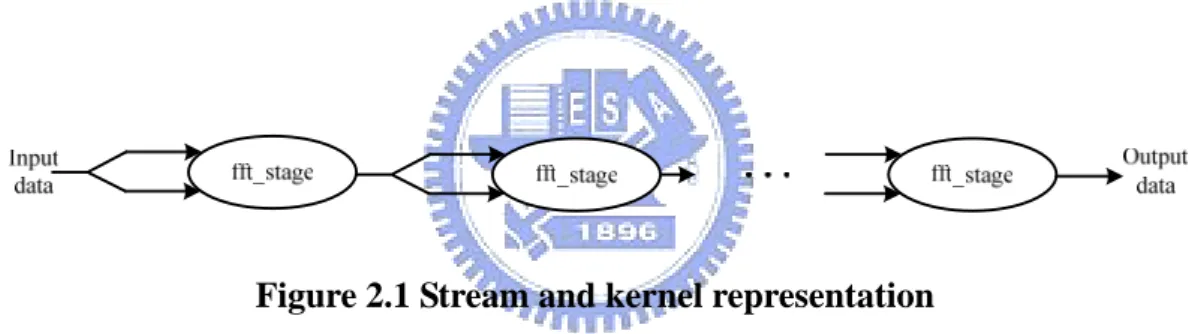
In Figure 2.1, shows the mapping of radix-2 FFT [7] to the stream model. Each oval in the figure corresponds to the execution of a kernel, while each arrow represents a data stream transfer. In the stream implementation, kernel requires two input streams and one output stream. The output of the last kernel is in bit-reversed order, so it must be reordered in the memory. In FFT only data elements passed between kernels need to access the SRF, and only the initial input data and final output data need to access the global memory space in DRAM.
Figure 2.1 Stream and kernel representation
Applications that are more involved than the FFT example map to the stream model in a similar fashion. Examples can be found in other references: Khailany et al. discuss the mapping of stereo depth extractor [5]; Rixner discusses the mapping of an MPEG-2 encoder [8]; and Owens et al. discuss the mapping of a polygon rendering pipeline [9].
The stream model is important because it organizes an application to expose the locality and parallelism information that is inherent in the application.
2.1.2 Stream micro-architecture
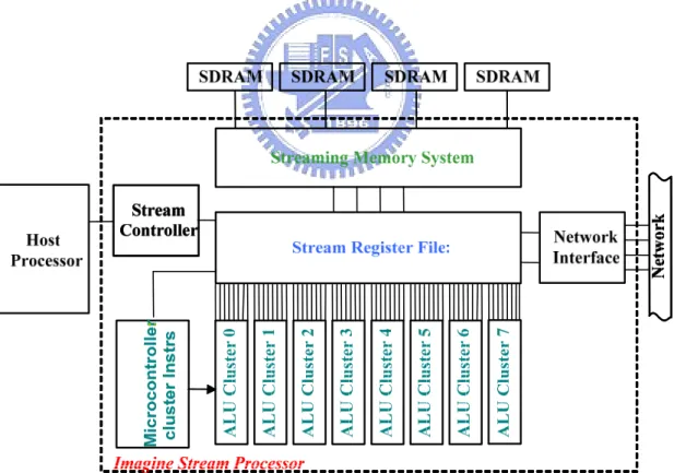
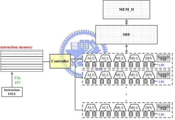
The stream processor is a hardware micro-architecture designed to implement the stream programming model. Imagine, designed by computer systems laboratory of Stanford University is a stream processor which block diagram is shown in Figure 2.2 [14]. The core of Imagine is a 128 KB stream register file (SRF). The SRF is connected to 8 SIMD-controlled VLIW-like arithmetic clusters controlled by a microcontroller, a memory system interface to off-chip DRAM, and a network interface to connect to other nodes of a multi-Image system. All modules are controlled by an on-chip stream controller under the direction of an external host processor.
The working set of streams is located in the SRF. Stream loads and stores occur between the memory system and the SRF; network sends and receives occur between the network interface and the SRF. The SRF also provides the stream inputs to kernels and stores their stream outputs.
The kernels are executed in the 8 arithmetic clusters. Each cluster contains several functional units (which can exploit instruction-level parallelism) fed by distributed local register files. The 8 clusters (which can exploit data-level parallelism) are controlled by the microcontroller, which supplies the same instruction stream to each cluster. On Imagine, streams are implemented as contiguous blocks of memory in the SRF or in off-chip memory. Kernels are implemented as programs run on the arithmetic clusters.
The three-level memory bandwidth hierarchy characteristic of media application behavior consists of the memory system, the SRF, and the local register files within the clusters
2.1.3 An example of stream processor: Imagine
Imagine is a programmable stream processor, which is a general purpose processor, and is the hardware implementation of the stream model. The concept of this micro-architecture is based on stream. Imagine is organized to take advantage of the locality and parallelism inherent in media applications. A block diagram of the micro-architecture is shown in Figure 2.2.
Imagine contains 48 ALUs [12], and a unique three level memory hierarchy design to keep the functional units saturated during stream processing. The three-tiered data bandwidth hierarchy consists of a stream memory system (2 GB/s), a global stream register file (32 GB/s), and a set of local distributed register files located
near the arithmetic units (544 GB/s). The 128 KB SRF at the center of the bandwidth hierarchy not only provides intermediate storage for data streams but also enables additional stream clients to be modularly connected to Imagine, such as streaming network interface. A single microcontroller broadcasts cluster instructions in SIMD fashion to all of the arithmetic clusters. Each of Imagine’s 8 arithmetic clusters consists of 6 functional units containing 3 adders, 2 multipliers, and a divide/square root. These units are controlled by statically scheduled cluster instructions issued by the microcontroller.
2.2 Current usage of micro-architecture simulator
In some relevant science projects to PIM (Processor In Memory) [10], there always exist some cases utilizing micro-architecture simulator. For example, in the DIVA (Data IntensiVe Architecture) project [11], it employed ”DIVA simulator” to simulate the operation of DIVA. In addition, the PIM project IRAM also makes use of ” IRAM Simulator” to simulate the performance of iRAM [11].
Since Stream Processor also belongs to PIM techniques, our goal becomes to discover the optimized stream micro-architecture for a specific media application without using the expensive hardware equipment. The micro-architecture simulator is designed for stream processor intended to simulate the performance of diverse media application executed in stream processor.
The project has been divided into three parts in our team, including a low power ALU cluster, memory management unit and address translation unit and the simulator design. The detail micro-architecture of the cluster has been decided during a low power cluster design, by surveying papers and considering the performance and hardware usage. As for simulation, it has been designed for the performance
evaluation of different hardware organizations. The micro-architecture in a cluster being evaluated is always the same, the only variable is the number of clusters. With micro-architecture simulator, the number of clusters and the memory hierarchy needed for dedicated micro-architecture can be easily decided, and the hardware processor can be implemented.
2.3 The importance of the micro-architecture simulator
Stream micro-architecture could be the main trend of media processor in the future! Different from the hardware design of the special-purpose processor, which is designed for the algorithm of specific application and thus can achieve the best performance only when executing its favored application, the stream processor not only possesses the advantage of the special-purpose processor to achieve very good performance for specified application, it but also has great flexibility to adjust hardware micro-architecture for arbitrary algorithm of application (the number of computation units and the size of on-chip memory) and thus can best utilize the hardware resources for desired application.
Since the stream micro-architecture for diverse media application is quite different, how to discover the optimized micro-architecture for desired application is definitely a big question! One intuitive way is to utilize hardware to implement every possible design and then we can practically measure its performance. However, it seems to be a very inefficient way to find optimized design since the cost of the hardware implementation could be very expensive! In addition, hardware
implementation may take a lot of time. Compared to hardware implementation, software simulation would be much faster, more efficient, and cheaper to achieve the same purpose. Inspired from this idea, here we present the micro-architecture simulator!
Since the e-Home project has been divided into three main parts, including hardware design of an ALU cluster, simulator design for hardware performance evaluation, and low-power technique needed on the whole stream micro-architecture. In this thesis, the part of simulator design has been focused, it is helpful to the hardware decision of the stream processor.
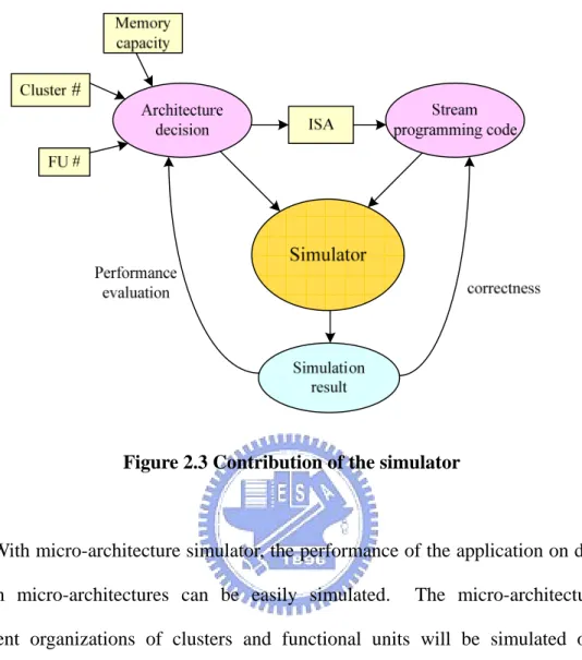
As shown in Figure 2.3, after micro-architecture decision step, application can be mapped into binary stream programming codes according to the ISA and instruction format of different functional units. Stream programming codes can be put into simulator to simulate the operation of which in stream processors, then the simulation result will be generated, which can be used to compare to the simulation result of other organization of micro-architectures and adjust the parameters that will affect the organization of stream micro-architecture till the optimal organization of micro-architecture is discovered. On the other hand, simulation result can also be used to make sure the correctness of the stream programming codes.
Figure 2.3 Contribution of the simulator
With micro-architecture simulator, the performance of the application on diverse stream micro-architectures can be easily simulated. The micro-architecture of different organizations of clusters and functional units will be simulated on the micro-architecture simulator. The simulation results will show:
1.) How many functional units (ALU, MUL, DIV) in every cluster are used. 2.) How many memory hierarchies in every level in every cluster are used. 3.) How much CPU time it will cost when executing application.
4.) The number of memory hierarchy in every level being used.
Then, the optimized hardware micro-architecture for specific application can be discovered based on these simulation results. The micro-architecture will efficiently lower the performance and will not increase too many data exchange of
low-bandwidth memory. The determination of the optimized hardware micro-architecture includes: number of clusters, number of functional units in a cluster, the size of memory hierarchy in every level.
Since the test-bench selected in this thesis is “FFT”, the micro-architecture needed to process this application is not that large enough. Time needed to access each level of memory hierarchy (SRF, SP, LRF) is almost the same, so the performance evaluated in this thesis depends only on the access time of each functional unit. However, micro-architecture simulator might be used for many other large applications in the future, time needed to access each level of memory hierarchy might be different. In that case, time to access each level of memory hierarchy have to be taken into consideration. The micro-architecture simulator designed in this thesis also has the function of evaluating the performance which takes memory access time into account, but the function is not suitable for the FFT’s micro-architecture.
Up to now, the stream micro-architecture has been widely explored to many media applications and explicitly demonstrated in many references, such as 3-D polygon rendering [9], MPEG-2 encoding [12], stereo depth extraction [13], and fast Fourier transform (FFT). In this paper, we shall choose FFT [14] as the benchmark to simulate the performance for specific hardware micro-architecture and then try to determine the optimized micro-architecture from these simulation data.
The micro-architecture design of the Simulator shall be explicitly depicted in Chapter 3. The demonstration of FFT on simulator and how we discover the optimized micro-architecture for FFT will be drawn in Chapter 4.
Chapter 3 Micro-architecture simulator
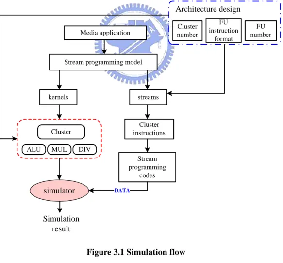
Figure 3.1 illustrates the whole simulation flow. In the Section 3.1, we shall introduce the whole micro-architecture of the simulator and the included components, and explain how simulator works. In Section 3.2, we shall detail the way to design the components inside the simulator, including cluster, functional unit, and memory hierarchy. In Section 3.3, we shall introduce how to utilize simulator to simulate hardware performance, that is, the whole simulation flow illustrated in figure above. The actual simulation performance shall be presented in Chapter 4.
Media application
Stream programming model
kernels streams
Cluster ALU MUL DIV
Cluster instructions Stream programming codes simulator DATA Architecture design Cluster number FU instruction format FU number Simulation result
3.1 Organization of the micro-architecture simulator
Figure 3.2 shows the block diagram of the simulator, which is a component of the simulation flow shown in Figure 3.1. Simulator is composed of a controller, many arithmetic clusters where the number of the clusters will differ from diverse application, three-tiered memory hierarchy (SRF, SP, and LRF), and instruction memory. It should be noted that the number of the components in the simulator is not fixed. It would depend on the demands of diverse media applications.
Figure 3.2 Block diagram of the micro-architecture simulator
Micro-architecture simulator is used to simulate the operation of the stream processor and the performance of the hardware micro-architecture. As shown in the flow of Figure 3.1, first, a multimedia application and then its hardware micro-architecture, including the number hardware and the memory size have to be
chosen. Then, this application is translated into the stream programming model, including kernel and stream, respectively. The cluster and its functional unit in Figure 3.2 are just the kernel for processing stream. In addition, the data being processed must be transformed into cluster instructions (stream) and then translate the cluster instructions into binary expression according to the instruction format defined by hardware.
Cluster instructions will be copied to instruction memory through File I/O. Controller will fetch instruction from instruction memory and equally distribute these cluster instructions to cluster for executing. Three kinds of registers, SRF, SP, and LRF, are used to save temporary results during computation process.
3.2 Design methodology of the micro-architecture simulator
In this section, the description on how to design the component of simulator, including Cluster, and functional unit (ALU, MUL, DIV) is presented.
3.2.1 Cluster
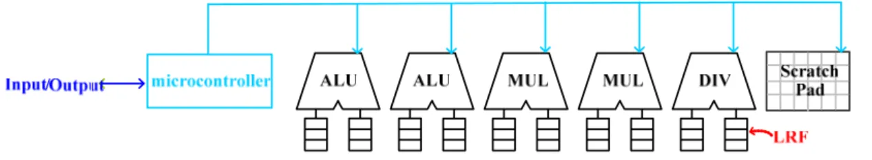
Figure 3.3 shows the block diagram of cluster. Cluster includes two ALU units, two MUL units, one DIV unit, and one 64 32-bit register, which is used to save data exchange between different units in the same cluster. Please note the size of SP register could vary according to the demands of diverse applications.
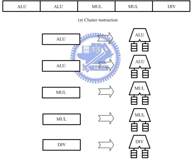
The main function of the component Cluster is to divide the received cluster instruction into multiple instructions that are processable by function units according to the number of functional units. As shown in Figure 3.4, cluster receives 137-bit cluster instruction. According to micro-architecture of the cluster, cluster instruction is divided into two 29-bit instructions for ALU, two 26-bit instructions for MUL, one 27-bit instruction for DIV.
3.2.2 ALU, MUL, DIV
In this section, how to design the functional unit shall be depicted. Since the main spirits for designing ALU, MUL, and DIV are basically the same, we shall focus on ALU to illustrate how to design functional unit. The only difference between these three components is the bit of “Opcode” needed for expressing the operation in the instruction format.
ALU
ALU is a two stage pipeline computation unit. Figure 3.5 shows the instruction format of ALU. The shadowed part in figure is Opcode field, which expresses the executing operation for instruction. Opcode also makes the biggest difference between these three functional units: ALU, MUL, and DIV. Please note that ALU requires more diverse operations. It demands 4-bits to express.
Figure 3.5 ALU instruction format
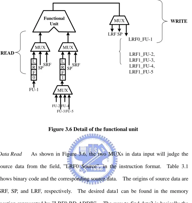
Figure 3.6 is the detail view of the functional unit and its associated register files. Roughly, it could be cataloged into three parts: data read, calculate, and write back.
READ Functional Unit MUX MUX MUX L R F 0 L R F 1 SPSRF SPSRF MUX FU-1 FU-2 FU-3 FU-4 FU-5 SP LRF LRF0_FU-1 LRF1_FU-2, LRF1_FU-3, LRF1_FU-4, LRF1_FU-5 WRITE
Figure 3.6 Detail of the functional unit
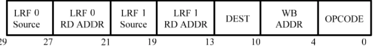
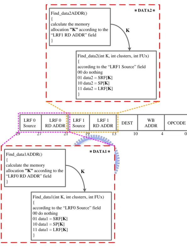
Data Read As shown in Figure 3.6, the two MUXs in data input will judge the source data from the field, ”LRF0 Source”, in the instruction format. Table 3.1 shows binary code and the corresponding source data. The origins of source data are SRF, SP, and LRF, respectively. The desired data1 can be found in the memory location represented by ”LRF0 RD ADDR”. The way to find data2 is basically the same as data1. The only difference is their reference fields. Acquiring data2 needs to take references of the information of ”LRF1 Source” and ”LRF1 RD ADDR”. Figure3.7 illustrates the program flow of how ALU in the simulator obtains two data resources, data1 and data2, according to the information of instruction.
LRF 0 Source LRF 1 Source LRF 0 RD ADDR LRF 1 RD ADDR DEST WB ADDR OPCODE 29 27 21 19 13 10 4 0 Find_data1ADDR() {
calculate the memory
allocation ”K” according to the “LRF0 RD ADDR” field }
Find_data1(int K, int clusterx, int FUx) {
according to the “LRF0 Source” field 00 do nothing 01 data1 = SRF[K] 10 data1 = SP[K] 11 data1 = LRF[K] } K DATA1 Find_data2ADDR() {
calculate the memory
allocation ”K” according to the “LRF1 RD ADDR” field }
Find_data2(int K, int clusterx, int FUx) {
according to the “LRF1 Source” field 00 do nothing 01 data2 = SRF[K] 10 data2 = SP[K] 11 data2 = LRF[K] } K DATA2
Table 3.1 Lookup table of the data source SP 10 LRF 11 SRF 01 None 00 Source Binary Code SP 10 LRF 11 SRF 01 None 00 Source Binary Code
Calculate The information describing what kind of operations is required to be execute by every instruction will be implicitly included in the final field “Opcode” of instruction. Different binary codes represent distinct operations. Table 3.3 shows the lookup table for opcodes and corresponding operations. Matching the instruction with those bits of opcode filed in the instruction format would know what kind of operation is required for specific instruction.
Table 3.3 Kernel ISA of ALU unit
EQ 1101 LE 1100 LT 1011 SRA 1010 SRL 1001 SLL 1000 NOT 0111 XOR 0110 OR 0101 AND 0100 ABS 0011 SUB 0010 ADD 0001 Operation OPCODE EQ 1101 LE 1100 LT 1011 SRA 1010 SRL 1001 SLL 1000 NOT 0111 XOR 0110 OR 0101 AND 0100 ABS 0011 SUB 0010 ADD 0001 Operation OPCODE
Write Back The computation results of the functional unit will determine the destination of write back through one MUX, including SRF, SP, and LRF. Write back to LRF is classified into two kinds. If the results have to write back to the same LRF of functional unit, it should be written back to LRF-0 (LRF0_FU-1). On the other hand, if the result have to write to other LRFs of functional unit, it should be written to LRF-1 (LRF1_FU-2, LRF1_FU-3, LRF1_FU-4, LRF1_FU-5). MUX determines the destination of write back according to the information in the field “DEST” of the instruction, and finds out the memory location of the write back from the field ”WB ADDR”. Table 3.2 shows the corresponding binary code and register of DEST. Figure 3.8 illustrates the write-back step of programming process, and Figure 3.9 illustrates the flow of programming process in ALU Unit.
Table 3.2 Look up table of the data write back destination of FU-1 LRF1_FU5 111 LRF1_FU4 110 LRF1_FU3 101 LRF1_FU2 100 LRF0_FU1 011 SP 010 SRF 001 None 000 DEST Binary Code LRF1_FU5 111 LRF1_FU4 110 LRF1_FU3 101 LRF1_FU2 100 LRF0_FU1 011 SP 010 SRF 001 None 000 DEST Binary Code
Find_WBDDR() {
calculate the writeback memory allocation ”K” according to the “WBADDR” field }
Writeback(int K, int clusterx, int FUx) {
according to the “DEST” field 000 do nothing 001 SRF[K] = result 010 SP[K] = result 011 LRF0_FU1[K] = result 100 LRF1_FU2[K] = result 101 LRF1_FU3[K] = result 110 LRF1_FU4[K] = result 111 LRF1_FU5[K] = result } *WriteBack* K 4. 4. Find_data1ADDR() {
calculate the memory allocation ”K” according to the “LRF0 RD ADDR” field
}
Find_data1(int K, int clusterx, int FUx) {
according to the “LRF0 Source” field 00 do nothing 01 data1 = SRF[K] 10 data1 = SP[K] 11 data1 = LRF[K] } *DATA1* K 1. 1. Find_data2ADDR() {
calculate the memory allocation ”K” according to the “LRF1 RD ADDR” field
}
Find_data2(int K, int clusterx, int FUx) {
according to the “LRF1 Source” field 00 do nothing 01 data2 = SRF[K] 10 data2 = SP[K] 11 data2 = LRF[K] } *DATA2* K 2. 2. calculate data1 data2 result
Figure 3.9 Block diagram of the ALU unit
MUL
MUL is a four-stage pipeline computation unit. The way MUL Unit deal with instruction is the same as that of ALU. The only difference is that MUL Unit just deal with one operation “multiple”. Therefore, only one-bit is required for “Opcode”
filed in the instruction format and the instruction length of MUL Unit is three-bit less than that of ALU Unit. Please not that the processing flow of ALU Unit in Figure 3.9 can be also applied to MUL Unit. However, in the third step, calculate, the opcode must be referred to the corresponding operation shown in Table 3.4.
Table 3.4 Kernel ISA of MUL unit
MUL 1 None 0 Operation OPCODE MUL 1 None 0 Operation OPCODE DIV
DIV is a six stage pipeline computation unit. Again, the way DIV Unit treats instruction is the same as that of ALU. The only difference lies in the operations executed by DIV Unit and ALU Unit. The operations which DIV Unit deal with are ”division”, “remainder”, and “exponent”, respectively. Therefore, only two-bit are required for “Opcode” field in instruction format expressing these three distinct operations. It follows that the instruction length of DIV Unit is two bit less than that of ALU Unit. The programming flow of ALU Unit in Figure 3.9 can then be applied again to DIV Unit except that the reference opcode in the third step, calculate, must take the reference of Table 3.5 to see the corresponding operation.
Table 3.5 Kernel ISA of DIV unit
SQR 11 REM 10 DIV 01 None 00 Operation OPCODE SQR 11 REM 10 DIV 01 None 00 Operation OPCODE
3.2.3 Memory hierarchy
Each level of memory hierarchy is implemented using global array.
1.) Instruction memory: Vary with different instruction number and cluster length. The size of instruction memory is defined as “instruction number multiplies VLIW_length”.
2.) SRF, SP, LRF: Assume each SRF, SP, and LRF is a sixty-four 32-bit register. It could vary with the demands of diverse media applications. Assume that ADDR_BIT needs six bits and the memory hierarchy sizes of SRF, SP, and LRF in the system are 64 registers, 64*Cluster_Number registers, and 64*2*FU_Number*Cluster_Number registers, respectively. Assume micro-architecture has 5-cluster, each cluster has four functional units, and ADDR_BIT = 6. It follows that the applicable memory hierarchy size SRF, SP, and LRF of in the application are 64 registers, 320 registers(64*5), and 2560 registers(64*2*4*5), respectively.
3.3 Mechanism of the micro-architecture simulator
The performance simulation flow of media application in micro-architecture simulator should be delineated in this section. In this paper, FFT is selected as the simulation benchmark.
Simulation Flow is shown in Figure 3.1, where the design for the kernel of stream programming mode, i. e., simulator, has been introduced in Section 3.2. The application of Simulator can be roughly classified into two stages:
1.) Determination of the simulation micro-architecture of the application. This step contains a number of parameters setups and shall be explicitly answered in Section 3.3.1.
2.) Plugging cluster instruction (stream) into simulator for simulating, and performance estimation shall be clarified in Section 3.3.2.
3.3.1 Parameter definition
Before the operation of the application to be simulated, the “micro-architecture decision” step in Figure 2.3 has to be accomplished, a couple of parameters establishing micro-architecture must be decided.
1.) The number of ALU, MUL, and DIV in a cluster: This step is to define the micro-architecture inside a cluster. If defining a cluster contains three ALU Units, two MUL Units, and one DIV Unit, then the cluster executing instruction would be like Figure 3.10. These parameters will determine the instruction length of cluster instruction, and the number of bit required for the ”DEST” field in the instruction format. If the number of the functional unit in a cluster lies between one to five, the DEST field only needs 3-bit to express the destination of result write back; If the number of the functional unit ranges from 6 to 13, the DEST field shall need 4-bit to represent.
Figure 3.10 Block diagram of a cluster
2.) Determine the number of cluster needed for micro-architecture.
3.) Determine sufficient number of SRF, SP, and LRF, and the number of bit of the ”ADDR_BIT” which expresses memory location in the instruction format. 4.) According to several parameters defined above, we then can calculate the length of ALU Unit, MUL Unit, and DIV Unit for dealing with instructions, and the length of cluster instruction.
ALU_BIT = 8 + 3*ADDR_BIT + DEST_BIT MUL_BIT = 5 + 3*ADDR_BIT + DEST_BIT DIV_BIT = 6 + 3*ADDR_BIT + DEST_BIT
VLIW_length = ALU_BIT*ALU_Number + MUL_BIT*MUL_Number + DIV_BIT*DIV_Number
5.) Determine the consumed clock cycles executed by every functional unit, “ALU_Time”, “MUL_Time”, and “DIV_Time”. The information is intended to calculate CPU Time.
3.3.2 Map application into dedicated binary stream programming codes
Based on the “micro-architecture decision” step in 3.3.1, ISA of the micro-architecture and the instruction format of different functional unit can be explicitly known. As can be seen in Figure 3.11, the function of traditional compiler is replaced by hand-coding method, which scheduling the instructions of the application according to the ISA into cluster instructions, then the cluster instructions is mapping into stream programming codes that can be executed on the stream processor according to the instruction format of the functional units.
Figure 3.11 Map the application into stream programming code
3.3.3 Simulation
As can be seen in Figure 2.3, after accomplishing two steps of the micro-architecture decision and mapping application into stream programming codes, which may be plugged into simulator to simulate the performance executed on the stream processor.
1.) Load the cluster instructions saved in the files into instruction memory using File I/O.
2.) According to the cluster number defined in Section 3.3.1, it would yield the same number of cluster objects as ”cluster_number”. Every cluster object represents one cluster in real micro-architecture. According to the numbers defined by ALU, MUL, and DIV in Section 3.3.1, every cluster object will declare the same numbers of ALU object, MUL object, and DIV object. These functional unit objects declared by every cluster stand for the functional units processing the instruction in the cluster of practical micro-architecture.
3.) Controller would fetch the cluster instructions in the instruction memory, and then equally distribute these instructions to clusters for dealing with instruction. 4.) The function of Cluster is to divide the cluster instruction into instructions of the same number as the number of functional unit in the cluster, and then submit these instructions into ALU/MUL/DIV for executing.
For example, if a cluster has two ALU, two MUL, and one DIV, we would divide a 137-bit cluster instruction into two 29-bit ALU instructions, two 26-bit MUL instructions, and one 27-bit DIV instruction, and then respectively submit them to five Functional Units for processing. Figure 3.4 clearly illustrates the functions of Cluster.
5.) Estimate Performance:
CPU Time Every time when the function, calculate(), is used in ALU, MUL,
and DIV, we accumulate the number of these function units being executed, i. e., ALU, MUL, and DIV, inside different cluster. According to ALU_Time, MUL_Time, and DIV_Time defined in Section 3.3.1, how many clock cycles every cluster will cost when it implement application could be estimated
further. Comparing to the time consumed by the cluster, the desired CPU Time for implementing application is just the maximum value being drawn.
Memory accessing times Every time when ALU, MUL, and DIV do data
fetch or data write back, memory hierarchy will be used. Simulator will accumulate the number of accessing for every memory hierarchy level (could be SRF, SP, or LRF). Application will show the employment information of memory hierarchy after simulator done its work.
The amount of each Memory hierarchy level being used The information
about the required amount of memory in every level for simulating application executed by stream processor will also show in the simulation results. This information can greatly help determining how much memory hierarchy capacity is required for the application.
3.4 Summary
In this chapter, how to design an micro-architecture simulator, how to simulate the process flow in stream processor of media application, and how to estimate its performance has been introduced. In Chapter 4, actually the performance of the media application, FFT, implemented in diverse hardware micro-architecture should be simulated, and then the optimized hardware micro-architecture for FFT should be selected according to the performance results.
Chapter 4 Performance Evaluation
In this chapter, FFT [15] is taken as benchmark and translated as application into stream programming model to evaluate the performance of the micro-architecture defined.
4.1 Benchmark
Media applications contain abundant parallelism and are computationally intensive. In recent decades, a wide variety of media applications have been simulated, such as stereo depth extractor, video encoder/decoder, polygon render and matrix QR decomposition. These media applications all bear a common characteristic: containing a large amount of data-level parallelism. All of these media applications will first be mapped into stream programming model. A stream program organizes data as streams and computation as sequence of kernels.
In the paper, 32-point Fast Fourier Transform (FFT) is selected for the benchmark. FFT is a kind of fast Discrete Fourier Transform (DFT). The formulation is shown in Equation 4.1. There are two reasons why FFT is selected as benchmark in this thesis. The first reason is that FFT is the most often used part in multimedia applications. The second reason is that in paper [15], FFT is taken as an example that executing on the Imagine, and the result of that is also discussed in the paper. So, it is meaningful to take FFT as the benchmark of micro-architecture simulator. 1 0 .2 / [ ] [ ] , 0 1 N kn N n j N N X k x n W k N W e π − = − = ≤ =
∑
g ≤ −First, FFT algorism has to be mapped into stream programming model. By casting media applications as stream programs, hardware is able to take advantage of the abundant parallelism, computational intensity, and locality in media applications.
4.2 Experimental set-up
4.2.1 Parameter definition
Before simulating FFT on simulator, a couple of parameters for determining stream micro-architecture have to be defined. These parameters have been introduced in Section 3.3.1.
1.) Number of function unit in a cluster: When the stream micro-architecture of
FFT is simulated, each cluster contains two ALU Units, two MUL Units, and one DIV Unit. Since cluster only has five functional units, the ”DEST” field requires only 3-bit for expressing.
2.) Cluster number: In this paper, we would pay our attention on 1-cluster,
2-cluster, 4-cluster, and 8-cluster micro-architecture to simulate the performance on the stream processor.
3.) ADDR_BIT: In the simulation of FFT, 6-bit memory allocation expression is
being adopted. In other words, the available space for memory hierarchy is SRF = 64 registers, SP = 64*Cluster_Number registers, and LRF = 640*Cluster_Number registers, respectively.
4.) Based on the cluster number, functional unit number, DEST_BIT, and
ADDR_BIT defined above, the length of every functional unit could be calculated for executing instruction, and the length of cluster instruction., where VLIW_Length = 137, ALU_BIT = 29, MUL_BIT = 26, and DIV_BIT = 27.
5.) Determine the required clock cycles for functional unit executing operation.
6.) ALU_Time = 2 cycles
7.) MUL_Time = 4 cycles
8.) DIV_Time = 6 cycles
4.2.2 Translate FFT algorism into stream code
As the simulation flow illustrated in Figure 3.1 shows, the selected media application is mapped into stream programming model. Kernel is simply the simulator introduced in Section 3.4. Therefore, FFT is translated into stream code for the convenience of simulating on simulator.
In this system, since there is no compiler to generate the corresponding stream code for FFT, hand coding method is taken to generate stream code of FFT. Before simulating the performance of FFT, the instruction of FFT should be created first. Then, the instruction should be scheduled to generate the cluster instructions that are executable by micro-architecture simulator. It should be noted that ALU unit needs two clock cycles to work while MUL unit requires four clock cycles. Moreover, FFT does not require the functional unit, DIV, and thus the function of DIV will not be explained in this section. It follows that the instruction formats, which are corresponding to cluster instructions, have to be translated into binary code. Finally, save these Binary codes are saved in a file called ”FFT.dat”.
4.2.3 Data loading from main memory
In addition to determining those parameters mentioned in Section 3.3.1, simulator will in advance load the necessary memory data into SRF, and LRF.
Since the purpose of stream micro-architecture is to decide how much space of hardware will be utilized before the stream micro-architecture is implemented on hardware, it could maximally exploit hardware to obtain the best performance maximally exploit hardware. Therefore, the memories that data consumes when performing FFT, i.e., the thirty-two x[n] in DFT, have been loaded on SRF in advance, and a number of indispensable parameters during computation have been loaded on LRF in advance, as well. As an example, during operation of FFT, there are many mathematical formulae regarding sin and cosine being used. Thus, a couple of corresponding values of sin and cosine will be loaded into LRF in advance.
Figure 4.1 shows the status of memory being utilized before the simulator executes. x[0]~x[31] are copied to SRF through load command. The LRF0 of MUL1 and MUL2 would also load some required parameters from memory, respectively.
Figure 4.1 Memory usage before simulation
After the necessary parameters and loading for memory data are determined, the simulator is ready to evaluate the performance.
4.3 Result of performance evaluation
In this section, performance evaluation for the stream micro-architecture of different cluster is discussed in detail.
4.3.1 1-cluster stream micro-architecture simulation
First of all, FFT instructions are scheduled as 1-cluster cluster instructions. There are 135 cluster instructions in total. Then, the instruction format definition shown in Figure 3.5 is referred to translate the cluster instructions into binary code, i.e., representation with 0’s and 1’s.
1-cluster micro-architecture (Figure 4.2): 1-cluster micro-architecture contains two ALU Units, two MUL Units, one DIV Unit, and five data exchange intermediate medium between functional units, SP, which are sixty-four 32bit registers. There are one LRF, sixty-four 32-bit registers, and one SRF, sixty-four 32-bit registers, at the input of every functional unit. Therefore, we could know that SRF is sixty-four 32-bit registers, SP is 64*1 = sixty-four 32-bit registers since there is only one cluster in the entire system, and LRF is 64*2*5 = six hundred and forty 32-bit registers in total since there are five FUs in a cluster and one cluster in the system.
Figure 4.2(a) Block diagram of 1-cluster micro-architecture simulator
Figure 4.2(b) Stream programming model of 1-cluster architecture
The cluster instructions initially saved in file ”fft.dat” will be read into Instruction memory through File I/O. The controller shown in Figure 4.3 will fetch cluster instructions from instruction memory, and then submit all cluster instructions to the only cluster for executing. The initial data x[0]~x[31] of FFT will be loaded into SRF through memory. The initial input of Functional unit would be derived from SRF. There are many intermediate computation results during the process from x[0] to X[0], where X[0] is the output of FFT. If these data are used in the same functional unit, these temporary results will be saved in LRF0 of the functional unit.
four functional units. Only the final calculation results, X[0]~X[31], will utilize SRF to write them back to Memory. The intermediate calculation results could take advantage of less time being consumed by LRF instead of memory to expedite whole computation speed.
Figure 4.3 shows the simulation results. It can be seen that executing one hundred and thirty-five cluster instructions require ALU Unit being used for 257 times, MUL Unit for ninety-six times, and DIV Unit for zero time since the operation of FFT does not need division. The whole operation of FFT requires four hundred and fort-nine clock cycles. In the meantime, SRF, SP, and LRF are accessed one hundred and thirty-seven times, one hundred and sixty-three times, and seven hundred fifty-nine times, respectively.
Since this micro-architecture has only one cluster, the time needed to execute FFT is the same as the clock cycles spent by Cluster 1. The ratio of this micro-architecture using memory hierarchy is SRF: SP : LRF = 59 : 11 : 74.
Figure 4.3 Simulation result of 1-cluster stream micro-architecture
4.3.2 2-cluster stream micro-architecture simulation
First of all, FFT instructions are scheduled as 2-cluster cluster instructions. 2-cluster micro-architecture is like dual CPU system. The system can deal with two cluster instructions in one clock. After scheduling, there are sixty-five cluster instructions for cluster 1, and 65 cluster instructions for cluster 2. After two clusters execute one hundred and thirty cluster instructions in total, the final results could be obtained. After scheduling instructions, like 1-cluster simulator, these one hundred and thirty cluster instructions have to be translated into binary codes that are implementable on simulator according to the instruction format shown in Figure 3.5.
2-cluster micro-architecture (Figure 4.4): There are two clusters in micro-architecture. The functional unit in each cluster contains two ALU Units, two MUL Units, one DIV Unit, and five data exchange intermediate medium between functional units, SP, which are sixty-four 32bit registers. The definition is like that of 1-cluster micro-architecture, which has been illustrated in Section 4.2.2. In addition, there are also one LRF, sixty-four 32-bit registers, at the input of every functional unit and one SRF, sixty-four 32-bit registers, in memory hierarchy. Therefore, it could be known that SRF is 64 32-bit registers, SP is 64*2= 128 32-bit registers since there are two clusters in the entire system, and LRF is 64*2*5*2 = 1280 32-bit registers in total since there are five FUs in a cluster and two clusters in the system.
ALU ALU MUL MUL DIV Scratch Pad
LRF MEM_D SRF Controller Instruction FILE File I/O
Instruction memory ALU ALU MUL MUL DIV Scratch Pad
LRF
Figure 4.4(b) Stream programming model of 2-cluster architecture
The cluster instructions initially saved in file ”fft.dat” will be read into instruction memory through File I/O. The controller shown in Figure 4.4 will fetch cluster instructions from instruction memory, and then equally distribute them to cluster 1 and cluster 2 for executing. The initial data x[0]~x[31] of FFT will be loaded into SRF register through memory. The initial data source of functional unit would be derived from SRF. However, there are many intermediate computation results during the process from x[n] to X[n], where X[n] is the output of FFT. If this result is the input of the functional unit of the same cluster, it will be written to registers LRF or SP. If the calculation result is taken as input of functional unit of the other cluster, then data would be submitted to the function unit of the other cluster through SRF register. Data exchange between every instruction would be processed in the same cluster as possible through faster LRF or SP. Only when data are exchanged between clusters will we use the SRF Register with slower access speed.
The final computation results X[0]~X[31], will be temporarily saved in SRF, and then be written back to memory through memory store command. With this idea to manipulate instructions could greatly save computation time.
Figure 4.5 shows simulation results of 2-cluster stream micro-architecture. Compared to 1-cluster micro-architecture in Section 4.3.1, it can be readily seen that the performance has been greatly improved when we utilize two clusters for processing the cluster instructions of FFT. As shown in figures, it could be observed that cluster 1 deals with sixty-five cluster instructions, uses ALU Unit for one hundred and twenty-seven times, MUL for twenty-two times, and never use DIV Unit since the operation of FFT does not need DIV Unit to implement instruction. The whole operation of FFT require one hundred and seventy-one clock cycles for cluster 1 processing sixty-five cluster instructions. In the meantime, SRF, SP, and LRF are accessed one eighty-one times, forty-eight times, and three hundred and eighteen times, respectively.
As shown in the figure, it could be observed that cluster 2 deals with sixty-five cluster instructions, uses ALU Unit for one hundred and twenty-nine times, MUL for seventy-four times, and never uses DIV Unit since the operation of FFT does not need DIV Unit to do instruction. The whole operation of FFT require two hundred and seventy-seven clock cycles for cluster 2 processing sixty-five cluster instructions. In the meantime, SRF, SP, and LRF have been accessed for one hundred and three times, one hundred and twenty-three times, and three hundred and eighty-three times, respectively.
Figure 4.5 Simulation result of 2-cluster stream micro-architecture
The time spent by 2-cluster stream micro-architecture for executing FFT instructions is just the maximal time spent by cluster1 and cluster 2, where the CPU_Time of cluster-1 = 171 clock cycles, and CPU_Time of cluster-2 = 277 clock cycles. Therefore, the CPU_Time spent in this system is 277 clock cycles (the maximal value). In addition, it could be observed that the ratio of the whole micro-architecture using memory hierarchy is SRF: SP : LRF = 62 : 6 : 116.
4.3.3 4-cluster stream micro-architecture simulation
First of all, schedule the FFT instructions as 4-cluster cluster instructions. 4-cluster micro-architecture is just like four-CPU system. The system can deal with four cluster instructions in one clock. After scheduling, every cluster needs to deal with forty-two cluster instructions. After four clusters execute one hundred and
sixty-eight cluster instructions for total, it could be obtained the final results. After scheduling instructions, just like 1-cluster simulator, these one hundred and thirty cluster instructions have to be translated into binary codes that are implementable on simulator according to the instruction format shown in Figure 3.5.
4-cluster micro-architecture (Figure 4.6): There are four clusters in micro-architecture. The functional unit in each cluster contains two ALU Units, two MUL Units, one DIV Unit, and five data exchange intermediate medium between functional units, SP, which is sixty-four 32-bit registers. The definition is just like that of 1-cluster micro-architecture, which has been illustrated in Section 4.2.2. In addition, there are also one LRF, sixty-four 32-bit registers, in the input of every functional unit and one SRF, sixty-four 32-bit registers, in memory hierarchy. Therefore, it could be known that SRF is sixty-four 32-bit registers, SP is 64*4= 256 32-bit registers since there are two clusters in whole system, and LRF is 64*2*5*4 = 2560 32-bit registers for total since there are five FUs in a cluster and four clusters in whole system.
ALU ALU MUL MUL DIV Scratch Pad LRF MEM_D SRF Controller Instruction memory Instruction FILE File I/O
ALU ALU MUL MUL DIV Scratch Pad
LRF
ALU ALU MUL MUL DIV Scratch Pad
LRF
ALU ALU MUL MUL DIV Scratch Pad
LRF
Figure 4.6(a) Block diagram of 4-cluster micro-architecture simulator
S R F Cluster 1 ALU 1 ALU 2 MUL 1 MUL 2 DIV SP 1 instruction Cluster 2 ALU 1 ALU 2 MUL 1 MUL 2 DIV SP 1 instruction ALU 1 ALU 2 MUL 1 MUL 2 DIV SP 1 instruction Cluster 3 ALU 1 ALU 2 MUL 1 MUL 2 DIV SP 1 instruction controller Cluster instructions Instruction memory S R F S R F S R F Cluster 4
The cluster instructions initially saved in file ”fft.dat” will be read into instruction memory through File I/O. The controller shown in Figure 4.6 will fetch cluster instructions from instruction memory, and then equally distribute them to cluster 1, cluster 2, cluster 3, and cluster 4 for executing. The initial data x[0]~x[31] of FFT will be loaded into SRF register through memory. The initial data source of functional unit would be derived from SRF. However, there are many intermediate computation results during the process from x[n] to X[n], where X[n] is the output of FFT. If this result is the input of the functional unit of the same cluster, it will be written to registers LRF or SP. If the calculation result is taken as input of functional unit of the other cluster, then the data would be submitted to the function unit of the other cluster through SRF register. Data exchange between every instruction would be processed in the same cluster as possible through faster LRF or SP. Only when data are exchanged between clusters, the SRF register with slower access speed will be used. The final computation results X[0]~X[31], will be temporarily saved in SRF, and then be written back to memory through memory store command. With this idea to manipulate instructions could greatly save computation time.
Figure 4.7 shows the simulation results of 4-cluster stream micro-architecture. Compared to 1-cluster micro-architecture in Section 4.3.1, it can be readily seen that the performance has been greatly improved when four clusters are utilized for processing the cluster instructions of FFT.
As shown in figures, it could be observes that cluster 1 deals with forty-two cluster instructions, uses ALU Unit for sixty-nine times, MUL for three times, and never use DIV Unit since the operation of FFT does not need DIV Unit to implement
instruction. The whole operation of FFT require seventy-five clock cycles for cluster-1 processing forty-two cluster instructions. In the meantime, SRF, SP, and LRF are accessed for fifty-five times, fifteen times, and one hundred and forty-six times, respectively.
As shown in figures, it could be observed that cluster 2 deals with forty-two cluster instructions, uses ALU Unit for sixty-four times, MUL for nineteen times, and never uses DIV Unit since the operation of FFT does not need DIV Unit to implement instruction. The whole operation of FFT require one hundred and forty-two clock cycles for cluster 2 processing forty-two cluster instructions. In the meantime, SRF, SP, and LRF are accessed for sixty-three times, thirty-nine times, and one hundred and forty-seven times, respectively.
As shown in figures, it could be observed that cluster 3 deals with forty-two cluster instructions, uses ALU Unit for sixty-eight times, MUL for thirty-three times, and never uses DIV Unit since the operation of FFT does not need DIV Unit to implement instruction. The whole operation of FFT require one hundred and thirty-four clock cycles for cluster 3 processing forty-two cluster instructions. In the meantime, SRF, SP, and LRF are accessed for seventy times, fifty-seven times, and one hundred and seventy-six times, respectively.
As shown in figures, it could be observed that cluster 4 deals with forty-two cluster instructions, uses ALU Unit for fifty-six times, MUL for forty-one times, and never uses DIV Unit since the operation of FFT does not need DIV Unit to implement instruction. The whole operation of FFT requires one hundred and thirty-eight clock cycles for cluster 4 processing forty-two cluster instructions. In the meantime, SRF, SP, and LRF are accessed for sixty-one times, fifty-nine times, and one hundred and seventy-one times, respectively.
Figure 4.7 Simulation result of 4-cluster stream micro-architecture
The time spent by 4-cluster stream micro-architecture for executing FFT instructions is just the maximal time spent by cluster 1, cluster 2, cluster 3, and cluster 4 where the CPU_Time of cluster 1 = 75 clock cycles, CPU_Time of cluster 2 = 102 clock cycles, CPU_Time of cluster 3 = 134 clock cycles, and CPU_Time of cluster 4 = 138 clock cycles. Therefore, the CPU_Time spent in this system is one hundred and thirty-eight clock cycles (the maximal value). In addition, it could be observed that the ratio of the whole micro-architecture using memory hierarchy is SRF: SP : LRF = 64 : 20 : 153.