國立交通大學
光電工程研究所
博士論文
氮化鎵材料發光二極體與面射型雷射之
製作與特性研究
Fabrication and Characteristics of
GaN-based Light-Emitting Diodes and
Vertical-Cavity Surface-Emitting Lasers
研 究 生: 朱 榮 堂
指導教授: 王 興 宗 教授
郭 浩 中 教授
國立交通大學
光電工程研究所
博士論文
氮化鎵材料發光二極體與面射型雷射之
製作與特性分析
Fabrication and Characteristics of
GaN-based Light-Emitting Diodes and
Vertical-Cavity Surface-Emitting Lasers
研 究 生: 朱 榮 堂
Student: Jung-Tang Chu
指導教授: 王 興 宗
Advisor: Shing-Chung Wang
郭 浩 中
Hao-Chung Kuo
氮化鎵材料發光二極體與面射型雷射之
製作與特性分析
Fabrication and Characteristics of
GaN-Based Light-Emitting Diodes and
Vertical-Cavity Surface-Emitting Lasers
研 究 生: 朱 榮 堂
Student: Jung-Tang Chu
指導教授: 王 興 宗
Advisor: Shing-Chung Wang
郭 浩 中
Hao-Chung Kuo
國立交通大學
光電工程研究所
博士論文
A dissertation
Submitted to Institute of Electro-Optical Engineering
College of Electrical Engineering and Computer Science
National Chiao Tung University
In Partial Fulfillment of the Requirements
For the Degree of
Doctor of Philosophy
In Electro-Optical Engineering
June 2008
Hsin-chu, Taiwan
氮化鎵材料發光二極體與面射型雷射之
製作與特性研究
研究生: 朱榮堂 指導教授: 王興宗 教授 郭浩中 教授國立交通大學光電工程研究所
摘要
由於氮化鎵基材發光元件可廣泛的應用於如指示燈、各種照明、光儲存等領 域,因此自 1960 年代以來氮化鎵相關材料成為世界上各研發團體的重要研究課 題之ㄧ,且在此數十年間氮化鎵材料與元件特性上有屢有重大的發現與進展。在 本研究論文中,我們製作氮化鎵發光二極體(LED)於金屬基板上與包含兩介電質 反射鏡的氮化鎵面射型雷射(VCSEL),並研究分析此二元件之主要特性。 首先我們製作大發光面積 (1x1 mm2 ) 藍光發光二極體於銅基板上。利用金 屬接合與雷射剝離製程,成長於sapphire 基板上之藍光發光二極體可以被轉移 至銅基板上。因具有良好的電流分佈,此大發光面積LED不需要透明電極便可以 提供均勻的發光圖形。且因銅基板為良好的導電與導熱材料,此LED可以操作高 至 1 安培且其光輸出功率呈線性增加。以在晶圓上(未切割及封裝)量測方式,此 LED 在 1 安培輸入電流的操作下,光輸出功率為 240 mW。 而當單一發光二極體的面積增大並於高電流操作時,則需要考慮電流聚集效 應(current crowding)對於元件光電特性之影響。依實驗結果得到的電流擴散長 度為 400 μm,我們針對銅基板上的大發光面積 LED 設計了不同的電極圖形以研 究電極圖形對於元件特性之影響。實驗結果顯示,設計良好的電極圖形可以提供極圖形之 LED 的光輸出功率為含有簡單圓形電極之 LED 的 4 倍。 另一方面,我們也提出了含有上下兩介電質反射鏡之氮化鎵面射型雷射結 構。利用雷射剝技術並沉積成長介電質反射鏡,我們可以製作一含有氮化鎵與氮 化銦鎵(GaN/InGaN)多量子井(MQW)的面射型雷射結構。在室溫下以一雷射(波長 為 355 nm)為激發光源,在光激發操作下,研究其發光特性。此氮化鎵面射型雷 射的Q 系數 (quality factor) 為 518,雷射波長為 415.9 nm,雷射頻譜之半高 寬為 0.25 nm。由頻譜半高寬的減小、雷射頻譜之極化率與在發光孔徑中的雷射 輻射圖形等結果,明確地顯示垂直雷射的行為。此氮化鎵面射型雷射於室溫下之 臨界條件為 270 nJ 且特徵溫度為 278 K,自發輻射係數約為 1x10⁻³ 。 我們也利用 Hakki-Paoli 方法量測並計算此面射型雷射之增益特性。在室溫 臨界條件時,光增益為 2.9x103 cm-1。在不同操作溫度下,我們發現越低溫時, 光增益隨著注入載子數目增加而增加的速率越大。線寬增加係數 (linewidth enhancement factor) 在室溫下為 2.8,其數值隨著操作溫度降而降低,溫度為 80 K時,線寬增加係數為 0.6。 此外,我們也觀察到當激發光源的能量增加時,在面射型雷射之發光孔徑中 會有數個相對於不同輻射波長的雷射亮點。利用微螢光激發(micro-PL)方式量測 發現在雷射發光孔徑中有螢光強度不均勻的現象。此一結果可以歸因於銦含量在 MQWs 中的不均勻分佈所造成。而銦含量的不均勻也造成在一個發光孔徑中所觀 察到的多個雷射亮點。 最後,我們提出一個雙介電質反射鏡電激發操作氮化鎵面射型雷射的結構, 並討論此電激發面射型雷射結構的製程與結果。
Fabrication and Characteristics of GaN-based
Light-Emitting Diodes and
Vertical-Cavity Surface-Emitting Lasers
Student: Jung-Tang Chu Advisor: Dr. Shin-Chung Wang
Dr. Hao-Chung Kuo
Department of Photonics & Institute of Electro-Optical Engineering
National Chiao Tung University
Abstract
Due to the widespread applications such as indicators, back lighting, ambient lighting, display, optical storage, optical communication, etc., the GaN-based light emitting devices are widely investigated and have many remarkable breakthroughs in performance. In this study, the fabrication of GaN-based light emitting diodes (LEDs) on a metal substrate and vertical-cavity surface-emitting lasers (VCSELs) with two dielectric mirrors are demonstrated. The characteristics and performance of the LEDs and VCSELs are analysed and characterized.
We demonstrated a large emission-area (1x1 mm2) blue LEDs on copper
substrate. The LEDs structure grown on sapphire substrate by metal organic chemical vapor deposition system was transferred onto a Cu substrate using bonding and laser
lift off techniques. The large emission-area LEDs showed a uniform light-emission pattern over entire defined mesa area without the transparent contact layer on the n-type GaN. The operating current of the LEDs can be driven up to 1000 mA with continuously increasing light output-power. Under wafer-level measurement, the light output-power is 240 mW with a driving current of 1000 mA.
As the area of a single LED chip is scaled up, the current crowding effect under high current operation should be considered, while the current spreading length in the LEDs on Cu is about 400 μm. For optimizing the n-electrode pattern, we observed and reported the effect of n-electrode patterns on the optical characteristics of the large emission-area. The light emitting patterns showed an obvious current crowding effect in the LEDs with a simple circular n-electrode pattern. The LEDs with well-designed n-electrode pattern showed a uniform distribution of light emission and a higher output power due to uniform current spreading. Under 1000 mA operation, the LEDs with a well-designed n-electrode showed about a 4-fold increase in the light output power over the LEDs with a simple circular n-electrode pattern.
On the other hand, we also proposed a GaN-bsed VCSEL structure consists of InGaN/GaN MQWs and two dielectric DBRs with high reflectivity. The GaN-based cavity including MQWs was gown on a sapphire substrate. Then the grown cavity was embedded by two dielectric DBRs and transferred onto a silica substrate.
The laser emission characteristics of a GaN-based vertical-cavity surface-emitting laser with two dielectric distributed Bragg reflectors were investigated under optically pumped operation at room temperature. The quality factor of the VCSEL is 518, indicating a good interfacial layer quality of the structure. The laser emits emission wavelength at 415.9 nm with a linewidth of 0.25 nm. The measurement results, including the linewidth reduction, degree of polarization of 70% and emission images confined inside apertures, clearly indicate a vertical lasing action. The laser has a threshold pumping energy of 270 nJ at room temperature and a characteristic temperature of 278 K. The VCSEL has a high spontaneous emission factor of about 1x10⁻³.
Meanwhile, Hakki-Paoli method was applied to analyze the temperature dependent optical gain and linewidth enhancement factor of the VCSELs. Due to multiple cavity modes in the structure, the optical gain can be obtained by measuring the photoluminescence spectra below the threshold condition. At room temperature, the optical gain of 2.9x103 cm-1 was estimated at the threshold condition with a carrier
density of 6.5x1019 cm-3. Under different ambient temperature, it is found that the gain
increases more rapidly as a function of the injected carrier density at lower temperature. The linewidth enhancement factor (α-factor) shows dependence on the wavelength and was smaller at shorter wavelength. The α-factor at room temperature
was estimated as 2.8 and decreased to as low as 0.6 at 80K. The characterization of temperature dependent gain and α-factor provides further understanding in operation of the GaN-based VCSEL.
The laser emission patterns show single and multiple emission spots spatially with different emission spectra under different pumping conditions. μ-PL intensity mapping indicated that the nonuniform PL emission intensity across the VCSEL aperture. The CL and TEM images of the as-grown cavity used in the VCSEL also showed the inhomogeneity of indium composition in the InGaN/GaN MQWs. The inhomogeneous material gain distribution resulting in nonuniform PL emission could be due to the fluctuated indium composition in the MQW active layers and result in multiple emission spots in an aperture.
In the final chapter, we presented a two dielectric DBRs VCSEL structure for current injection operation. The issues of modifying the fabrication and design for the proposed VCSELs structure were also characterized and discussed.
致謝
碩士班與博士班共七年在交通大學光電工程研究所的時光裡有幸得到許多 人在各方面的指導與協助。 感謝指導教授王興宗老師與郭浩中老師的指導。王老師除了在學術研究上嚴 肅並認真地給予學生指導與討論之外,最令人難忘的就是王老師爽朗的笑聲與過 於常人的精力。感謝王老師教導我嚴謹的研究方法與研究態度,還有授予我豐富 的學識。感謝郭浩中老師的指導與鞭策,許多研究工作才得以完成。 感謝盧廷昌老師的指導與對於實驗內容及結果的討論。也特別要感謝交通大 學材料所的吳耀銓教授,在架設實驗設備與實驗方法上的指導。 還要感謝同實驗室的朱振甫博士在實驗上的協助與指導,感謝林佳鋒博士、 姚忻宏博士、 張亞銜博士、賴芳儀博士、薛道鴻博士、黃泓文博士、高志強博 士在實驗上的協助。以及實驗室歷屆的研究生與博士生們的幫助,讓我的研究得 以順利進行。另外,與實驗室成員們在生活上的相處也讓我得到精神上的滿足與 歡愉。 感謝我重要的家人,我的母親與三位兄長全方面的支持。 感謝研究生過程中所有曾經予以我協助的所有人,有以上諸位的協助與我個 人些許的努力,此論文才得以完成。 再次感謝所有人幫助我取得博士學位並完成此論文。Contents
Abstract (in Chinese) I Abstract III Acknowledgement VII Contents VIII List of tables XI List of figures XII
Chapter 1 Introduction
...11.1 GaN-based materials and light-emitting diodes...1
1.2 GaN-based laser diodes...4
1.3 An overview of the dissertation...6
Reference
Chapter 2 Fundamental of GaN-based light emitting device
...142.1 Light emitting diodes...14
2.1.1 Issues involved in GaN-based LEDs on sapphire substrate...14
2.1.2 GaN-based LEDs on copper substrate...16
2.2 Vertical-cavity surface-emitting lasers...18
2.2.1 Fundamental of VCSELs...18
2.2.2 Obstacles in achieving a GaN-based VCSEL...19
2.3 An approach: laser lift-off technique...22
Reference
Chapter 3 Large emission-area GaN-based blue LEDs
………..….283.1 Fabrication of large emission-area vertical LEDs...28
3.2 Characteristics of large emission-area vertical LEDs...31
3.3 Current spreading length...32
3.4 Effects of different n-electrode patterns on characteristics of the large emission-area LEDs...33
Reference
Chapter 4 GaN-based Vertical-Cavity Surface-Emitting Lasers
...534.1 Structure design and simulation...53
4.1.1 Distributed Bragg reflector...53
4.1.2 Resonant Cavity...57
4.2 Fabrication of the GaN-based VCSEL with two dielectric DBRs...59
Chapter 5 Performance and characteristics of the two dielectric DBR
GaN-VCSELs
...745.1 Measurement setup...74
5.2 Threshold condition and spectrum evolution...74
5.3 Temperature dependent threshold...79
5.4 Temperature dependent gain characteristics...80
5.5 Effect of Indium inhomogeneity on laser characteristic...84
Reference
Chapter 6 Summary and future works
...1086.1 Summary...108
6.1.1 Large emission-area LEDs on Cu substrate...109
6.1.2 Two dielectric DBRs VCSELs...110
6.2 Future works...112
Reference
Publication list
...119List of tables
Chapter 3
Table 3.1 Electrical and thermal properties for several materials used in this
dissertation...42
Table 3.2 Detailed dimensions of the four electrode patterns...47
Chapter 4
Table 4.1 Maximum reflectivity corresponding to pair numbers for SiO2/TiO2,
List of figures
Chapter 1
Figure 1.1 Lattice constant as a function of bandgap energy of III-V nitride
compounds...8
Chapter 2
Figure 2.1 Schematic diagram of a conventional GaN-based LED on a sapphire
substrate...24
Figure 2.2 Basic geometry of a vertical-cavity surface-emitting laser...25
Chapter 3
Figure 3.1 Schematic fabrication steps of the large-area GaN LEDs on Cu
substrate...38
Figure 3.2 Schematic diagram of the fixture for metal bonding process...40
Figure 3.3 SEM image of the n-GaN surface after LLO process. Arrows indicate
some of the Ga droplets left by the decomposition of GaN...41
Figure 3.4 Schematic structure of the large-area emission LED on Cu...43
Figure 3.6 (a) L-I-V characteristics of the large-area-emission GaN LEDs on Cu
substrate under continuous-wave operation. (b) Electroluminescence of the LLO-LED under a driving current of 200 mA...45
Figure 3.7 Normalized emission intensity as a function of the distance from the
electrode edge. Inset shows the micrograph of the optical emission from the LED driven at 200 mA...46
Figure 3.8 The schematic diagrams top view of the LED devices with four
different n-electrode patterns...47
Figure 3.9 L-I characteristics of LED a under cw and pulse operations with
various duty cycles...48
Figure 3.10 Light emission patterns and intensity distributions of the LEDs with
different n-electrode patterns...49
Figure 3.11 3-D isometric plot of the spatial intensity distribution of the LED a,
LED b, LED c and LED d with different electrode patterns
respectively...50
Figure 3.12 L-I characteristics of the LEDs with four different n-electrode
Chapter 4
Figure 4.1 The transmission matrix can be determined by solving Maxwell’s
equation at the interfaces of layer b...61
Figure 4.2 Schematic of distributed Bragg reflector incorporating m pairs of two
mediums with indices n1 and n2...62
Figure 4.3 Numerically determined spectral reflectivity R(λ) for SiO2/TiO2
DBRs with different number of pairs...63
Figure 4.4 Numerically determined spectral reflectivity R(λ) for SiO2/Ta2O5
DBRs with different number of pairs...64
Figure 4.5 The layer structure used for calculation of standing wave patterns.
The structure was constructed according to the fabricated dielectric DBRs VCSLEs...66
Figure 4.6 The simulated standing wave (square of electric field) patterns inside
the cavity for the dielectric DBRs VCSEL structure...67
Figure 4.7 PL spectrum of the as grown cavity consists of 10 pairs of 5 nm GaN
barriers and 3 nm In0.1Ga0.9N wells...68
Figure 4.8 Measured spectral reflectivity of 6 pairs of SiO2 and TiO2 DBR and 8
pairs SiO2/Ta2O5 DBR...69
after LLO and polishing process...70
Figure 4.10 Schematic fabrication steps of the GaN-based dielectric DBRs
VCSEL...71
Figure 4.11 (a) A photograph of the fabricated VCSEL on a silica host substrate.
(b) Microscopic image of a fabricated 2x2 VCSEL array. The circular areas are the locations of VCSELs with DBRs, also serving the emission apertures...72
Chapter 5
Figure 5.1 Schematic diagram of measurement setup for the characteristics of
the GaN-based two dielectric DBRs VCSEL...88
Figure 5.2 Laser emission intensity obtained from the emission spectra as a
function of pumping energy at room temperature...89
Figure 5.3 Spectral evolution of the VCSEL emission different pumping
level...90
Figure 5.4 Spontaneous emission spectrum below threshold condition shows
multiple cavity modes...91
Figure 5.5 Laser emission intensity as a function of normalized pumping
Figure 5.6 2-D contour plot (a) and 3-D isometric plot of the spatial intensity
distribution of the laser beam from the VCSEL...93
Figure 5.7 The angle dependent laser intensity...94
Figure 5.8 Temperature dependence of the lasing threshold of the VCSEL...95
Figure 5.9 Normalized photoluminescence spectra of the GaN-based VCSEL
under different pumping power levels at 300K...96
Figure 5.10 Gain spectra of the VCSEL under different pumping power levels at
300K...97
Figure 5.11 Pumping carrier density dependence of the peak gain of the lasing
mode (at ~420 nm) for different measurement temperature...98
Figure 5.12 The g0 factor as a function of temperature...99
Figure 5.13 Calculated α-factors as a function of wavelength for different
measurement temperature...100
Figure 5.14 Emission pattern of the VCSEL at pumping energies of (a) 1.15Eth
with single laser emission spot and (b) 1.2Eth with two laser
emission spots. The arrows indicate the position of the first and second emission spots. (c) Spectra of the first emission spot and second emission spot at pumping energies of 1.15Eth and 1.2Eth,
Figure 5.15 (a) Micro-PL intensity mapping image of the VCSEL aperture. (b)
Fine micro-PL scan inside the square area in (a)... 102
Figure 5.16 PL spectra of bright point (A) and dark point (B) areas...103
Figure 5.17 Monochromatic CL map of the as-grown InGaN MQWs sample at
410 nm...104
Figure 5.18 TEM image of the as-grown MQWs used in the VCSELs
cavity...105
Chapter 6
Figure 6.1 Schematic diagram of the two dielectric DBRs VCSEL structure for
electrical driving...115
Figure 6.2 SEM image of the two dielectric DBRs VCSEL structure...116
Figure 6.3 Emission images of the two dielectric VCSEL structure operated
Chapter 1 Introduction
After the single-crystlline gallium nitride bulks were demonstrated in late 1960s
[1.1], the development of III–V nitride compound have induced much advertence and have great progress. GaN based-compound with wide band gap and possible emission wavelength ranging from red to ultra-violet make it a compelling material system for light emitting devices application. GaN-based shot-wavelength devices, such as blue light-emitting diodes (LEDs) and laser diodes (LDs), are required for a number of applications, including solid-state lighting, full-color electroluminescent displays, laser printers, read-write laser sources for high-density information storage on magnetic and optical media, and sources for short-distance optical communications. The solid-state lighting is the most high-profile and desired application of the GaN-based materials due to the high luminaire efficiency, reliability and durability of the semiconductor light-emitting devices.
1.1 GaN-based materials and light-emitting diodes
III-V nitride-based semiconductors have a direct band gap that is suitable for blue light-emitting devices. The bandgap energy of aluminum gallium indium nitride (AlGaInN) varies between 6.2 and 1.89 eV, depending on its composition (Fig. 1.1).
Thus, red- to ultraviolet-emitting devices are possible to be fabricated by using AlGaInN. The first main progress in III–V nitride-based semiconductors was the use of AlN [1.2, 1.3] or GaN [1.4, 1.5] nucleation layers for the GaN growth. Using these nucleation layers, high-quality GaN films with a flat surface, a high mobility and a strong photoluminescence (PL) intensity could be obtained. The second important progress was realization of p-type GaN and understanding of the reason why p-type GaN had not been obtained. For the LEDs and LDs p/n layers are used to inject holes and electrons into the active layers, therefore, both p-type and n-type conductivity control are required to fabricate those devices. N-type GaN was easy to form but it was impossible to obtain p-type GaN films for a long period [1.6, 1.7]. In 1989, Amano et al [1.8] obtained p-type GaN films using Mg-doping for the acceptor impurity and a post low-energy electron-beam irradiation (LEEBI) treatment by means of metal organic chemical vapour deposition (MOCVD) growth method. After the growth, LEEBI treatment was performed for Mg-doped GaN films to obtain a low-resistivity p-type GaN film. In 1992, Nakamura et al [1.9, 1.10] obtained p-type GaN films with a resistivity of 2 Ωcm [1.9] using post N2-ambient thermal annealing
for Mg-doped GaN. The third main progress was the growth of InGaN film. InGaN is the most important compound semiconductor among III–V nitride compounds because InGaN active layers emit light by the recombination of the injected electrons
and holes in the InGaN. In 1992, Nakamura and Mukai [1.11] grew high-quality InGaN films for the first time which emitted a strong band-to-band emission from green to ultraviolet (UV) by changing the In content of InGaN using MOCVD system. Finally, an InGaN multiquantum-well (MQW) structure and confirmed an enhanced strong PL intensity from the quantized energy levels of the InGaN well layer with a thickness of 25 Å for the first time [1.12]. A small amount of indium added to the GaN is very important for obtaining a strong band-to-band emission because GaN without the indium cannot emit a strong bandto-band emission at room-temperature. This reason is considered to be related to deep localized energy states [1.13-1.17]. After these major techniques were developed, blue-green InGaN single-quantum-well (SQW) structure LEDs was demonstrated in 1994 [1.18].
Substrate is also an important issue for III-V ntride material growth. Comparing to the GaAs material system, GaN-based substrate generally have a large lattice mismatch. Sapphire has been used for GaN growth, despite the large lattice mismatch (13%; shown in Fig. 1.1). The crystal structure of GaN grown on sapphire is wurtzite. SiC is a more proper candidate for the substrate for GaN since it has small lattice mismatch for GaN. However, the cost of a SiC substrate is very expensive. Therefore, sapphire becomes a suitable and alternative substrate for GaN growth.
(IEQ) and light extraction efficiency (LEE) of GaN-based LEDs. Textured or roughened surface [1.20; a], substrate shaping [1.21], thin-film LED [1.22], flip-chip LED [1.23] and photonic crystal on LED [1.24] ect. were proposed to improve the light extraction efficiency. In the meanwhile, current blocking layer [1.25] and current spreading layer [1.26] in GaN-based LEDs, superlattice structure in the n-type cladding layer [1.27] and AlN/sapphire [1.28] were reported to reduce dislocation or defect and improve the light extraction efficiency.
1.2 GaN-based laser diodes
After the demonstration of InGaN QW LEDs, the RT violet edge-emitting laser (EEL) with InGaN MQW/GaN/AlGaN-based heterostructures under pulsed operation were achieved [1.19]. After that, many groups have reported pulsed operation of EELs
[1.29-1.35]. The latter results have shown that the lifetime became as long as and 10,000 hours [1.36] under RT continuous-wave (CW) operation. Also, high-power LDs were fabricated using epitaxially laterally overgrown GaN (ELOG) [1.37] and GaN substrates [1.38]. At present day (2007), the violet/blue EELs lasing at 400-410 nm with an optical output power of 200 mW have become commercial products mainly used in optical storage system [1.39].
lasers in device structure, is another type of semiconductor lasers. The VCSEL structures, in particular with a small optical mode volume can emit a single longitudinal mode with a symmetrically circular beam and a small beam divergence that are superior than the edge emitting lasers and desirable for many practical applications in high density optical storage, laser printing, etc. In addition to the practical applications, the strong cavity field in the VCSEL microcavity can facilitate the investigation of the cavity quantum electrodynamics effect such as single photon and polariton emission, controlled spontaneous emission, and low threshold or thresholdless lasing [1.40-1.42]. The realization of GaN-based VCSEL has attracted many attention after the edge-emitting LDs were demonstrated. Several groups have reported optically pumped GaN-based VCSELs using different kinds of vertical resonant cavity structure [1.43-1.45]. Due to the obstacles of obtaining a proper reflector and fabrication process, the electrical operated GaN-based VCSELs are not achieved for a long period after the EELs were demonstrated. A breaking through of demonstrating an electrical operated GaN-VCSEL was reported by S. C. Wang et al
1.3 An overview of the dissertation
Chapter 2 outlines the GaN-based light emitting devices including LEDs and VCSELs. Conventional LEDs structure grown on sapphire substrate and the issues of sapphire substrate are discussed. Laser-lift off technique for transferring a LED on sapphire to a metal substrate is described. The motivation and advantage of fabricating GaN-based thin film LEDs on metal substrates are resented. Ingredients of a laser/VCSEL structure are addressed and discussed. We discuss the obstacles of fabricating a GaN-based VCSEL and overview the three main types of prpoerted GaN-based VCSELs. The reasons for using VCSEL structure with two dielectric mirrors in the dissertation are presented. Basic theory of laser lift-off technique used in our work is reviewed and introduced.
Chapter 3 presents the fabrication steps of the large emission-area GaN-based LEDs on Cu substrate. Characteristics of the LEDs are shown and studied. The current spreading length in the LEDs on Cu is measured and analysed. Effects of current crowding on the performance of the LEDs are characterized. Different patterns of n-type pads are designed to characterize the influence of current spreading length and current crowding effect on the performance of the LEDs.
Chapter 4 shows the structure and designing issues of the GaN-based VCSELs with two dielectric mirrors. The spectral reflectivity of the SiO2/TiO2 and SiO2/Ta2O5
DBRs are calculated by transfer matrix method. The standing optical field in the resonant cavity were also simulated in order to design the epitaxial structure for obtaining a optimal optical gain. The fabrication steps of the two dielectric DBRs VCSELs are also demonstrated.
Chapter 5 shows the performance of the optically pumped GaN-based VCSEls. The threshold condition, cavity Q factor, characteristic temperature, polarization of the laser emission, gain and linewidth enhancement factor are characterized and discussed. The inhomogeneous indium composition in the InGaN/GaN MQWs are observed. Effects of the indium inhomogeneity on the characters of the VCSELs are investigated.
In the final chapter, chapter 6, an overview of this dissertation and directions of future works are given and proposed.
Figure 1.1 Lattice constant as a function of bandgap energy of III-V nitride compounds. 0 1 2 3 4 5 6 7 2.4 2.6 2.8 3.0 3.2 3.4 3.6 3.8 Lat ti c e const a nt ( A )
Sahhpire (0001)
SiC (6H)
Bandgap energy (eV)
InN
References
[1.1] H. P. Maruska and J. J. Tietjen: Appl. Phys. Lett. 65, 520 (1969) [1.2] S. Yoshida, S. Misawa and S. Gonda: Appl. Phys. Lett. 42, 427 (1983)
[1.3] H. Amano, N. Sawaki, I. Akasaki and T. Toyoda: Appl. Phys. Lett. 48, 353 (1986)
[1.4] S. Nakamura and G. Fasol: The Blue Laser Diode (Heidelberg: Springer, 1997)
[1.5] S. Nakamura: Jpn. J. Appl. Phys. 30, L1705 (1991)
[1.6] S. Strite and H. Morko: J. Vac. Sci. Technol. B 10, 1237 (1992) [1.7] F. A. Ponce and D. P. Bour: Nature 386, 351 (1997)
[1.8] H. Amano, M. Kito, K. Hiramatsu and I. Akasaki: Japan. J. Appl. Phys. 28, L2112 (1989)
[1.9] S. Nakamura, T. Mukai , M. Senoh and N. Iwasa: Japan. J. Appl. Phys. 31, L139 (1992)
[1.10] S. Nakamura, N. Iwasa, M. Senoh and T. Mukai: Japan. J. Appl. Phys. 31, 1258 (1992)
[1.11] S. Nakamura and T. Mukai: Jpn. J. Appl. Phys. 31, L1457 (1992)
[1.12] S. Nakamura , T. Mukai, M. Senoh, S. Nagahama and N. Iwasa: J. Appl. Phys.
[1.13] S. Chichibu, T. Azuhata, T. Sota and S. Nakamura: Appl. Phys. Lett. 69, 4188 (1996)
[1.14] S. Chichibu, T. Azuhata, T. Sota and S. Nakamura: Appl. Phys. Lett. 70, 2822 (1997)
[1.15] Y. Narukawa, Y. Kawakami, Sz Fujita, Sg Fujita and S. Nakamura: Phys. Rev. B 55, 1938 (1997)
[1.16] Y. Narukawa, Y. Kawakami, M. Funato, Sz Fujita, Sg Fujita and S. Nakamura: Appl. Phys. Lett. 70, 981 (1997)
[1.17] S. Chichibu, K. Wada and S. Nakamura: Appl. Phys. Lett. 71, 2346 (1997) [1.18] S. Nakamura, T. Mukai and M. Senoh: Appl. Phys. Lett. 64, 1687 (1994) [1.19] S. Nakamura, M. Senoh , S. Nagahama, N. Iwasa, T. amada, T. Masushita, H.
Kiyoku and Y. Sugimoto: Jpn. J. Appl. Phys. 35, L74 (1996)
[1.20] C. Huh, K. S. Lee, E. J. Kang and S. J. Park: J. Appl. Phys. 93, 9383 (2003) [1.21] Compound Semiconductors 7(1), 7 (2001).
[1.22] W. S. Wong and T. Sands: Appl. Phys. Lett. 75, 1036 (1999)
[1.23] J. J. Wierer, D. A. Steigerwald, M. R. Krames, J. J. O’Shea, M. J. Ludowise, G. Christenson, Y.-C. Shen, C. Lowery, P. S. Martin, S. Subramanya, W. Gotz, N. F. Gardner, R. S. Kern, and S. A. Stockman: Appl. Phys. Lett. 78, 3379 (2001)
[1.24] J. Shakya, K. H. Kim, J. Y. Lin and H. X. Jiang: Appl. Phys. Lett. 85, 142 (2004)
[1.25] C. Huh, J. M. Lee, D. J. Kim, and S. J. Park: J. of Appl. Phys. 92, 2248 (2002)
[1.26] J. K. Sheu, G. C. Chi, and M. J. Jou: Phot. Tech. Lett. 13, 1164 (2001)
[1.27] S. Nakamura, M. Senoh, S. Nagahama, N. Iwasa, T. Yamada, T. Matsushita, H. Kiyoku, Y. Sugimoto, T. Kozaki, H. Umemoto, M. Sano and K. Chocho: Appl. Phys. Lett. 72, 211 (1998)
[1.28] T. Egawa, H. Ohmura, H. Ishikawa and T. Jimbo: Appl. Phys. Lett. 81, 292 (2002)
[1.29] K. Itaya: Japan. J. Appl. Phys. 35, L1315 (1996)
[1.30] G. E. Bulman, K. Doverspike , S. T. Sheppard, T. W. Weeks, H. S. Kong, H. M. Dieringer, J. A. Edmond, J. D. Brown, J. T. Swindell and J. F. Schetzena: Electron. Lett. 33, 1556 (1997)
[1.31] M. P. Mack, A. Abare, m. Aizcorbe, P. Kozodoy, S. Keller, U. K. Mishra, L. Coldren and S. DenBaars: 1997 MRS Internet J. Nitride Semicond. Res. 2 41 (available from http://nsr.mij.mrs.org/2/41/)
[1.32] A. Kuramata, K. Domen, R. Soejima, K. Horino, S. Kubota and T. Tanahashi: Jpn. J. Appl. Phys. 36, L1130 (1997)
[1.33] F. Nakamura et al 1998 J. Crystal Growth 189/190 84
[1.34] M. Kneissl, D. P. Bour, N. M. Johnson, L. T. Romano, B. S. Krusor, R. Donaldson, J. Walker and C. D. Dunnrowicz: Appl. Phys. Lett. 72, 1539 (1998)
[1.35] H. Katoh, T. Takeuchi, C. Anbe, R. Mizumoto, S. Yamaguchi, C. Wetzel, H. Amano, I. Akasaki, Y. Kaneko and N. Yamada: Jpn. J. Appl. Phys. 37. L 444 (1998)
[1.36] S. Nakamura: Japan. J. Appl. Phys. 36, L1568 (1997) [1.37] S. Nakamura: Japan. J. Appl. Phys. 37, L627 (1998) [1.38] S. Nakamura: Japan. J. Appl. Phys. 37, L309 (1998) [1.39] http://www.nichia.com/
[1.40] M. Pelton, C. Santori, J. Vuckovic, B. Zhang, G. S. Solomon, J. Plant, and Y. Yamamoto: Phys. Rev. Lett. 89, 233602 (2002)
[1.41] H. Deng, G. Weihs, C. Santori, J. Bloch, and Y. Yamamoto: Science 298, 199 (2002)
[1.42] T. Kobayashi, T. Segawa, A. Morimoto, and T. Sueta: presented at 43rd Fall Meet. Japan Society of Applied Physics, Tokyo, September, 1982
[1.43] J. M. Redwing, D. A. S. Loeber, N. G. Anderson, M. A. Tischler, and J. S. Flynn: Appl. Phys. Lett. 69, 1 (1996)
[1.44] T. Someya, K. Tachibana, J. Lee, T. Kamiya, and Y. Arakawa: Jpn. J. Appl. Phys. 37, L1424 (1998)
[1.45] Y.-K. Song, H. Zhou, M. Diagne, I. Ozden, A. Vertikov, A. V. Nurmikko, C. Carter-Coman, R. S. Kern, F. A. Kish, and M. R. Krames: Appl. Phys. Lett.
74, 3441 (1999)
[1.46] T. C. Lu, C. C. Kao, H. C. Kuo, G. S. Huang, and S. C. Wang: Appl. Phys. Lett. 92, 141102 (2008)
Chapter 2 Fundamental of GaN-based light emitting device
2.1 Light emitting diodes
2.1.1 Issues involved in GaN-based LEDs on sapphire substrate
In GaN-based materials, the choice of the substrate for epitaxial growth is a considerable issue since the lattice-matched GaN substrate is not easily available. Sapphire has been used for GaN growth, despite the large lattice mismatch (13%). The crystal structure of GaN grown on sapphire is wurtzite. SiC is a more proper candidate for the substrate for GaN since it has small lattice mismatch for GaN (3.5%). However, the cost of a SiC substrate is very expensive. Therefore, sapphire becomes a suitable and alternative substrate for GaN growth. A regular GaN-based LED grown on sapphire substrate is depicted in Fig. 2.1. A blue LED basically consisting a n-GaN layer, multiple quantum wells layer, and a p-GaN layer. Since the sapphire is an electric insulator, a part area of LED should be etched to exposure the n-GaN for depositing the n-contact metal. The transparent contact layer (TCL) used for current spreading is necessary because of the high resistivity of the p-GaN layer [2.1]. The light generated from the MQWs is emitted from the p-GaN side.
There are some notable issues in the regular GaN-based LED structures. In order to deposit n-contact metal, a part area of the LED is etched from p-GaN layer to
n-GaN layer. For a LED mesa with 350x350 μm2 in area, about 10% area be etched is
necessary. In other words, 10% light emission area is sacrificed. The emission light pass through the TCL will be absorbed. The typical transmittance for commonly used TCL, Ni/Au or indium tin oxide (ITO) is 85% and 90% [2.2, 2.3], respectively. The emitted light from the MQWs goes down to the sapphire side is not effectively extracted outside the LED. The refractive indices of GaN and sapphire are 2.48 and 1.78, respectively. The reflectivity of the interface of n-GaN and sapphire therefore can be estimated by the equation,
2 ⎟ ⎟ ⎠ ⎞ ⎜ ⎜ ⎝ ⎛ + − = sapphire GaN sapphire GaN n n n n R
, the reflectivity can be estimated as about 3%. Only 3% of the downward (to the sapphire side) light is reflected upward to the p-GaN side.
As a LED is operated, the heat will be generated as the current injected into the device. For a LED on sapphire substrate, the generated heat can not be dissipated easily due to the poor thermal conductivity of sapphire (35 W/mK). The heat could increase the junction temperature of the LED, consequently saturate the light output power and degrade the reliability of the LED.
As show in Fig. 2.1, due to the p-contact and n-contact are on the same side of the sapphire substrate, the current path from p-contact to the n-contact is partly lateral. Due to this geometry, the finite resistance of the n-type material of the GaN buffer and
lower confinement layer causes the current to ‘‘crowd’’ near the edge of the contact
[2.4-2.7]. The current crowding effect becomes noticeable especially under high injection current density operation. It has also been shown experimentally that the current crowding increases with LED aging [2.5].
2.1.2 GaN-based LEDs on copper substrate
According to the above discussed issues, a GaN-based LED on an electric conductive substrate with high reflectivity and high thermal conductivity is desired. However, for III-V nitride material, the substrate with these features is nearly unavailable. In this study, we present a method to transfer the GaN-based LED structure grown on sapphire substrate to an electrical conductive, high-reflectivity and high-thermal conductivity host substrate and to fabricate blue LEDs on it.
The host substrate used in this study is copper (Cu). Because the Cu is electric conductive, the n- and p-contact can be deposited on the LED and Cu substrate dividedly. The etching process for depositing the n-contact on n-GaN is not necessary and therefore the emission area of LEDs can be more used efficiently. In addition, because the p and n contacts are deposited on the different sides of the LED structure, the injected current can flow vertically through the LED structure. Vertical current flow can reduce the current crowding effect and spread the injected current uniformly
over the LED devices. The uniform current spreading is more significant for high current density operation and could scale up the dimensions of a single LED chip (above 1x1 mm2) for the demand of high brightness for solid lighting application.
By inserting a metal layer between the LED film and the Cu substrate, the light emitted toward the metal reflector can be reflected upward to the outside of the LED. The light extraction efficiency could be improved by the reflected light. Since Cu has a high thermal conductivity value of 385 W/mK, the heat generated as operation can be dissipated more efficiently to improve the internal quantum efficiency and reliability of LEDs.
2.2 Vertical-cavity surface-emitting lasers
2.2.1 Fundamental of VCSELs
Diode lasers, like the other types of lasers, incorporate the following three ingredients. (1) Gain medium: The gain medium consisting of a material which normally absorbs incident radiation over some wavelength range of interest. But, if it is pumped by inputting either electrical or optical energy, the electrons within the material can be excited to the higher, nonequilibrium energy level, so that the incident radiation can be amplified rather than absorbed by stimulating the de-excitation of these electrons along with the generation of additional radiation. If the resulting gain is sufficient to overcome the losses of some resonant optical mode of the cavity, this mode is said to have reached threshold, and relatively coherent light will be emitted. (2) Pumping source: Pumping source provides the energy that can excite the electrons within gain medium at lower energy level to higher energy level. It could be either optical or electrical energy. (3) Resonant cavity: The resonant cavity provides the necessary positive feedback for the radiation being amplified, so that a lasing oscillation can be established and sustained above threshold pumping level.
Diode lasers are distinguished from the other two types lasers (gas lasers and solid-state lasers) mainly by their ability to be pumped by an electrical current. This results in a higher efficient operation. Power conversion efficiency of ~50% is
commonly for diode lasers, whereas efficiencies for the gas and solid-state lasers are commonly 1~10%.
As depicted in Fig. 2.2, the structure of most VCSELs consist of two parallel reflectors which are distributed Bragg reflectors (DBRs) and a cavity including a multiple quantum wells (MQWs) served as active layer. The reflectivity necessary to reach the lasing threshold should normally be higher than 99.9%. The electrode pads are for injecting electrons and holes effectively into the active region is necessary for a current injection device. Corresponding to the ingredients of a laser, the active layer is the gain medium that amplify the optical radiation in the cavity; the top DBR, bottom DBRs and cavity form a resonant cavity where the radiation can interact with active region and have positive feedback; the electrode pads is for current injecting into the cavity to serve as pumping source.
2.2.2 Obstacles in achieving a GaN-based VCSEL
In the GaN-based VCSEL structure, a micro cavity with a few λ in the optical thickness and a pair of high reflectivity (above 99%) distributed Bragg reflectors (DBRs) are necessary for reducing the lasing threshold. A difficulty in fabricating monolithically grown GaN-based VCSELs is the growth of high reflectivity epitaxial DBRs, which require a large number of AlGaN/GaN pairs to reach a high reflectivity
owing to the small difference in refractive index (~0.1) between the AlGaN/GaN pairs. In addition, the requirement of high reflectivity and high quality DBRs using AlxGa1-xN and GaN materials is quite formidable since these two materials have large
lattice mismatch and difference in thermal expansion coefficients that tends to form cracks in the epitaxially grown DBR structure. These cracks in DBR could result in the reduction of reflectivity due to scattering, diffraction and absorption. The crystalline quality of the multiple quantum wells (MQWs) grown on the DBRs would also be degraded because of the cracks. Recently, several groups have reported optically pumped GaN-based VCSELs mainly using three different kinds of vertical resonant cavity structure forms: (1) monolithically grown vertical resonant cavity consisting of epitaxially grown III-nitride top and bottom DBRs (epitaxial DBR VCSEL), (2) vertical resonant cavity consisting of dielectric top and bottom DBR (dielectric DBR VCSEL). (3) vertical resonant cavity consists of an epitaxially grown III-nitride top DBR and a dielectric DBR (hybrid DBR VCSEL). In 1996, Redwing et
al. proposed an all epitaxial DBR VCSEL structure consisting of a 10-μm GaN
microcavity embedded by two epitaxially grown 30-pair Al0.12Ga0.88N/Al0.4Ga0.6N
DBRs [2.8]. The reflectivity of top and bottom DBR is 93% and 84%, respectively. Although the reflectivity of the DBR was not very high, a stimulated emission with a wavelength of 363 nm was observed due to the thick gain layer (10-μm GaN). In
1998, Arakawa et al. grew an InGaN multiple quantum wells (MQWs) on 35-pair Al0.34Ga0.66N/GaN DBR and deposited a 6-pair SiO2/TiO2 on the grown structure
forming the hybrid DBR VCSEL structure [2.9]. The stimulated emission with 381 nm in wavelength and linewidth smaller than 0.1 nm were observed as the pumping power was above the threshold condition at 77 K. Cavity quality factor Q of the resonant cavity was estimated to be 165. Thereafter, in 1999, Song et al. demonstrated a dielectric DBR VCSEL structure consisting of InGaN MQWs and 10-pair HfO2/SiO2 top and bottom DBR using laser left-off technology [2.10]. The reflectivity
of top and bottom DBRs were 99.5% and 99.9%, respectively. The emission wavelength and linewidth of the resonant cavity tested at room temperature were 437 nm and 0.7 nm, respectively. Because of the high reflectivity DBRs, the cavity had a high Q factor of 600. In 2005, Feltin et al. showed that the Al1-yInyN/GaN material
system could be well suited to the growth of vertical cavity structures [2.11] because Al1-yInyN (y = 0.17) was lattice-matched to GaN thus avoiding the subsequent
appearance of additional structural degradation (new dislocations and/or cracks) while presenting a refractive index contrast around 7–8%, where the DBR requires over 40 pairs to reach a reflectivity of 99%. Their VCSEL structure consisted of InxGa1-xN/GaN (x = 0.15) MQWs and 28 (bottom)/23 (top) AlInN/GaN DBRs and
performance characteristics of optically pumped GaN VCSELs.
2.2.3 GaN-based VCSELs with two dielectric mirrors
In this study we propose a VCSEL structure consisting two dielectric DBRs and a GaN-based resonant cavity. An epitaxially grown, thick (~4 μm) GaN-based cavity incorporated with InGaN MQWs was separated from the sapphire substrate by using laser liftoff and then embedded the cavity between two dielectric DBRs. By using different dielectric materials with large difference in refractive index (for example, the difference in SiO2 and TiO2 is ~1.58 at 430 nm), a DBR with a high reflectivity and
wide stop band could be achieved with less DBR pairs.
2.3 An approach: laser lift-off technique
The bonding energies of the III-V nitrides are relatively high compared to other III-V compounds. The bonding energy of GaN is high as 8.92 eV/molecule, results in the higher melting temperatures and good thermal stability of the GaN compounds compared to other compound semiconductors. Groh et al. [2.12] reported the activation energy for GaN decomposition to be 3.25 eV/atom. They also observed the presence of Ga droplets during decomposition in vacuum indicating the GaN decomposes into solid gallium and gaseous nitrogen. Sun et al. [2.13] found the
thermal decomposition of MOCVD grown GaN on r-plane sapphire occur at a temperature of 1000 oC in a hydrogen ambient. Their report indicated decomposition
of the GaN→2Ga(l)+N2(g) will occur at a critical temperature of ~1000 oC at
atmospheric pressure [2.12, 2.14].
In this dissertation, a KrF excimer laser with a wavelength of 248 nm (5 eV) was used to decompose the GaN grown on c-plane sapphire. The laser illuminated on the surface between GaN and sapphire and decomposed the GaN into Ga and Ni2, hence,
the grown GaN-based LED or micro-cavity structure were transferred from the sapphire substrate to host substrate.
p-GaN
n-GaN
MQWs
p-contact
n-contact
TCL
Sapphire
Figure 2.1 Schematic diagram of a conventional GaN-based LED
Top DBR
Bottom DBR
Electrode pad
Electrode pad
Cavity
MQWs
Substrate
Light output
Reference
[2.1] S. Nakamura and G. Fahsol: The Blue Laser Diode (Springer, Berlin, 1997) [2.2] S. Y. Kim, H. W. Jang, and J. L. Lee: Appl. Phys. Lett. 82, 61 (2003) [2.3] T. Margalith, O. Buchinsky, D. A. Cohen, A. C. Abare, M. Hansen, S. P.
DenBaars, and L. A. Coldren: Appl. Phys. Lett. 74, 3930 (1999) [2.4] X. Guo and E. F. Schubert: J. of Appl. Phys. 90, 4191 (2001) [2.5] I. Eliashevich, Y. Li, and A. Osinsky: Proc. SPIE 3621, 28 (1999)
[2.6] G. H. B. Thompson: Physics of Semiconductor Laser Devices (Wiley, New York, 1980)
[2.7] S. Fujita, M. Funato, and D. C. Park: MRS Internet J. Nitride Semicond. Res. 4S1, G6.31 (1999)
[2.8] Joan M. Redwing David A. S. Loeber and Neal G. Anderson Michael A. Tischler and Jeffrey S. Flynn: Appl. Phys. Lett. 69, 1 (1996)
[2.9] T. Someya, K. Tachibana, J. Lee, T. Kamiya and Y. Arakawa: Jpn. J. Appl. Phys. 37, L1424 (1998)
[2.10] Y.-K. Song, H. Zhou, M. Diagne, I. Ozden, A Vertikov, A. V. Nurmikko C. Carter-Coman, R. S. Kern, F. A. Kish, and M. R. Krames: Appl. Phys. Lett.
74, 3441 (1999)
[2.11] J.-F. Carlin, J. Dorsaz, E. Feltin, R. Butté, N. Grandjean, M. Ilegems, and M. Laügt: Appl. Phys. Lett. 86, 031107 (2005)
(1974)
[2.13] C.J. Sun, P. Kung, A. Saxler, H. Ohsato, E. Bigan, and M. Razeghi, J. Appl. Phys.
76, 236 (1994)
[2.14] M. E. Lin, B. N. Sverdlov, and H. Morkoç: Appl. Phys. Lett. 63, 3625 (1993)
Chapter 3 Large emission-area GaN-based blue LEDs
3.1 Fabrication of large emission-area vertical LEDs
The LED structure was grown by metalorganic chemical vapor deposition (MOCVD) on a c-plane (0001) sapphire substrate. The LED structure consists of a 3-μm-thick n-type GaN layer, a region of multiple quantum wells (MQWs) consisting of five pairs of In0.25GaN0.75 well (3nm) and GaN barrier (10nm), and a 100-nm-thick
p-type GaN layer. Figures 3.1(1)-3.1(9) shows the fabrication steps of the large-area GaN LEDs with wafer bonding and laser lif-off (LLO) techniques. A SiN layer with 1 μm in thickness was deposited on the GaN LED wafer by a plasma enhanced chemical vapor deposition (PECVD) system. The SiN layer was then patterned as square mesas 1000x1000 μm2 in size by stander lithography and dry etching process.
With the SiN square mesas served as etching masks, the LED mesas were formed by etching the area without SiN masks to the sapphire substrate with an inductively coupled plasma reactive ion etching (ICP-RIE) system. After remove the SiN masks, a SiN layer (300 nm) serve as passivation layer was deposited on the LED mesas and p-GaN of the LED was explored by removing the SiN on the top of mesas. Then Ni/Au/Ni (20 nm/20 nm/250 nm) were deposited on the top of the mesas. The first two Ni/Au layers and the final Ni layer serve as contact metals for p-GaN and
bonding metal, respectively. Before bonding process, the metals-coated GaN LED was initially cleaned by surface treatment process as follow:
(1) Cleaned by acetone (ACE) in ultrasonic bath for removing particle and/or organic contamination on sample surface;
(2) Dipped in methanol (CH3OH) bath for hydrophilic treatment;
(3) Rinsed in de-ionized water (D.I. water) 3minute for surface clean; (4) Blowing with N2 gas for drying.
After cleaning, the metals-coated sample and the Ni-coated Cu substrate were pre-mounted together in D.I. water to avoid particles in air. The pre-mounted sample was then blown by N2 gas for drying and subsequently put into a fixture as depicted in
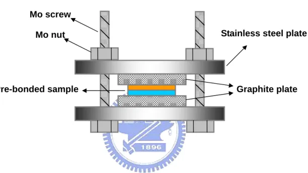
Fig. 3.2. This fixture consists of two stainless steel plates, molybdenum (Mo) scres and nuts, and high purity graphite plates. The fixture was then loaded in a stainless-steel tube chamber, which could be sealed and be filled with gaseous argon which was used to prevent oxidation of GaN and Cu samples during thermal treatment. As the chamber heated to 400 oC the compressive stress between the GaN
LED and Cu substrate increased due to different thermal expansion (Table 3.1) between the various materials that comprise the fixture. The estimated pressure applied on the sample is on the order of few MPa/cm2 by theory calculation. The
materials could not be determined by calculation because both the samples and the fixture underwent plastic deformation at some temperature during the process cycle
[3.1]. The bonded structure was then subjected to the LLO process. A KrF excimer laser at a wavelength of 248 nm with an energy density of 400 mJ/cm2 was used to
remove the sapphire substrate. The laser with a beam size of 1.2 mm × 1.2 mm was incident from the polished backside of the sapphire substrate onto the sapphire/GaN interface to decompose GaN into Ga and N2. In this process, the beam size of KrF
laser was larger than that of the size of the LEDs. Therefore, the laser irradiation on the interface of sapphire and GaN was uniform. After the backside of the GaN LED structure on the sapphire substrate was decomposed by the laser beam, an n-GaN/MQW/p-GaN/Ni/Au/Ni structure was formed on the Cu substrate. After LLO process, the decomposition of GaN left Ga droplets on the surface of n-GaN as show by Fig. 3.3. Then the sample was dipped into HCl solution to remove residual Ga droplet on the n-GaN. Finally, patterned Ti/Al layers were deposited on n-GaN as an n-type contact without additional semitransparent contact layer. The final structure of the large emission area LED on Cu is depicted as Fig. 3.4.
3.2 Characteristics of large emission-area vertical LEDs
The scanning electron microscope (SEM) image of the transferred GaN LED on Cu substrate is shown in Fig. 3.5. A complete and smooth LED film without peeling or cracks was observed on the Cu substrate despite the large difference in thermal expansion coefficients of GaN (4.4 × 10⁻⁶K-1) and Cu (16.9 × 10⁻⁶K-1). A smooth and
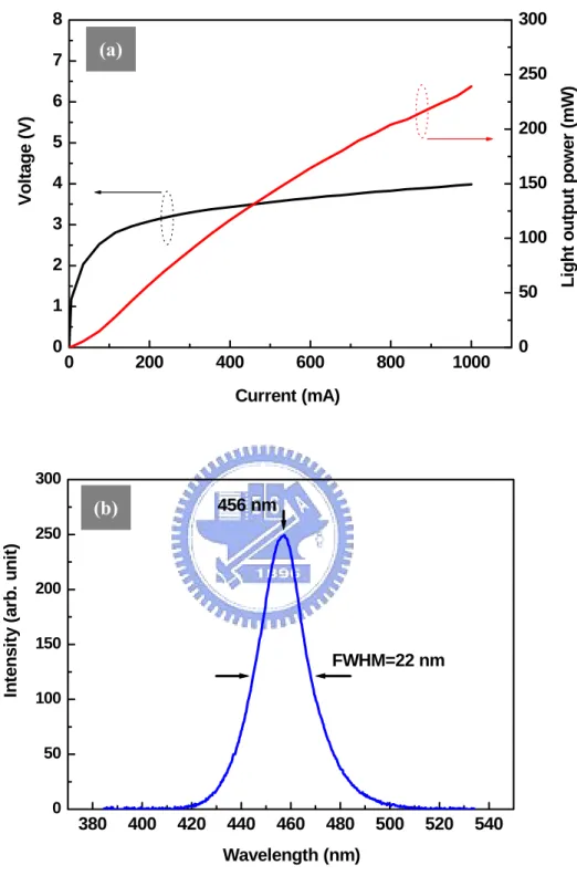
adhesive bonding interface was also observed. These results are essential to provide good optical and electrical characteristics of the LLO-LEDs. Figure 3.6(a) shows the light output power-current-voltage (L-I-V) characteristics of the large-area-emission GaN LEDs on Cu substrate under continuous-wave operation. The L-I-V characteristics were measured with an on-wafer testing configuration, consisting of the Si detector mounted directly above the LED and the driving current being applied through two probes (anode and cathode). The light output power showed continuous increasing as the driving current was increased from 0 to 1000 mA. The high thermal conductivity of the Cu substrate (401 W/mK at 300 K) and the large area of the device enable high current operation without pronounced power saturation. The maximum output power is 240 mW with driving current of 1000 mA. The well behavior of I-V characteristics was also observed. The voltage of the LLO-LED at 350 mA is 3.5 V.
Figure 3.6(b) shows electroluminescence of the LLO-LED under a driving current of 200 mA. The peak wavelength is 456 nm and the full width at half maximum (FWHM)
is 22 nm.
3.3 Current spreading length
Because the mobility of electrons in n-GaN is higher than that of holes in p-GaN
[3.3], the injected current is supposed to distribute more uniformly in p-down LLO-LEDs than that in p-up LEDs on sapphire. However, as the size of p-down LLO-LEDs are scaled up and the driving current is increased, the current spreading length in the device need to be concerned for a uniform optical emission pattern. The current spreading length is an important parameter as designing the pattern of electrode pad especially in a large area GaN-LED. The pattern of electrode should be designed by taking the current spreading length into consideration for providing a uniform current spread.
The current spreading length can be estimated since there is no transparent layer for enhancing current spread in our large-area p-down LEDs. A circular electrode with a diameter of 120 μm was deposited on the center of the 1x1 μm2 p-down
large-area LED. A micrograph of the optical emission from the LED driven at 200 mA is shown as the inset of Fig. 3.7. The micrograph clearly reveals that the emission intensity decreases with increasing distance from the electrode edge. The curve shows the experimental normalized intensity as a function of the distance from
the electrode edge. Since the emission intensity is proportional to the current density, the current spreading length can be defined as the distance that the emission intensity decreases to 1/e (about 36.8%) of the maximum intensity [3.4]. The result indicates that the current spreading length in the p-down LED is about 400 μm under 200 mA operation. Therefore, a simple circular electrode pattern is not sufficient for providing a uniform current distribution in the large-area p-down LEDs.
3.4 Effects of different n-electrode patterns on characteristics of
large-area LEDs
In the p-side-down LLO-LED configuration, the n-GaN layer serves as a better current spreading layer than the p-GaN layer in the p-side-up configuration on a sapphire substrate due to the higher electron mobility and greater thickness of the n-GaN layer. Since the light emission intensity is directly proportional to the current density, a uniform current distribution in a n-GaN layer to provide a uniform light emission pattern is necessary. In this section, four different geometric n-electrode patterns were deposited on large-area p-side-down LLO-LEDs of 1000×1000 μm2 in
dimensions. The current crowding effect in the p-side-down GaN LLO-LEDs under high current injection level was observed and studied. The light emission patterns of LEDs with different n-electrode patterns are compared. The
electrode-pattern-dependent light output power is also discussed.
The fabrication process of the large-area p-down LEDs was same as mentioned in previous section. In the final step of deposition of n-electrode pad, Ti/Al layers with different patterns were deposited on the n-GaN layers as an n-type contact without additional transparent contact layers. The schematic top view of the LED devices with four different n-electrode patterns is shown in Fig. 3.8. The detailed dimensions of each electrode pattern are shown in Table 3.2.
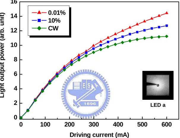
In Fig. 3.9 the light output-current (L-I) characteristics of LED a under continuous-wave (cw) and pulse operations with various duty cycles are compared. Under the same driving current operation, the light output power increased as the operation duty cycle was decreased from cw to 0.01% as shown in the figure. The output power saturation is also less pronounced as the duty cycle is decreased. The inset shows the micrographic surface light emission pattern of LED a driven at 100 mA. The injected current crowded near the electrode, resulting in an area with a higher current density corresponding to the brighter area around the circular contact indicated by the surface light emission pattern of LED a. The crowded current could induce thermal and carrier over flow effects [3.4-3.7] which saturate and decrease the output power of the LEDs. The thermal effect induced by current crowded around the electrode is one reason for the power saturation of LED a as suggested by the L-I
characteristics for different operation duty cycles.
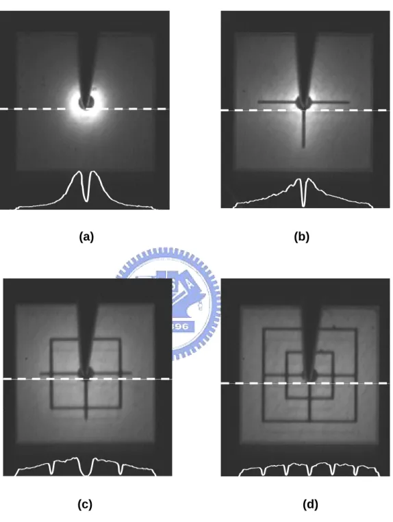
In order to reduce the current crowding effect and investigate the influence of the n-electrode pattern on optical characteristics, different n-electrode patterns were designed for the LLO-LEDs. Surface light emission patterns of the four LEDs with different n-electrode are shown in Fig. 3.10. The light emission patterns were obtained and analyzed at a driving current of 450 mA using a near-field microscope with a charge-couple device and a video analyzer (BeamView Analyzer, Coherent Inc.) linked to a computer. The solid curves at the bottom of the images stand for the relative light output intensity measured along the dashed lines. The light intensity was normalized with the peak values, normally appearing at the edges of the circular electrodes in the four LEDs. In Fig. 3.10(a), the light emission close to the circular electrode shows great intense intensity, which reveals that the injection current crowded around the electrode pad. In the absence of a transparent contact layer for current spreading, the n-electrode of LED a is insufficient to provide uniform current spreading in the large-area p-side-down LEDs configuration. In Fig. 3.10(b), more intense light emission around the extended cross-shaped electrode is observed. With the cross-shaped electrode for enhancement of current spreading, the distribution of light emission was more uniform compared with that of LED a, as shown by the relative intensity curve. The extended cross-shaped electrode improved the current
spreading over the large-area mesa and consequently provided a more uniform light emission pattern. The light emission patterns of the LEDs with two other electrodes are shown in Figs. 3.10(c) and 3.10(d). The light intensity of LED d showed a uniform distribution from the center to the edge of the mesa. In contrast, the light intensity of
LED c decreased near the edge of the mesa. The light emission pattern of LED d is
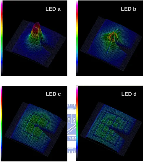
more uniform than that of LED c, in which a more intense emission appeared inside the square electrode. Figure 3.11 shows the 3-D isometric plot of the spatial intensity distribution of the LEDs with different electrode patterns. The isometric plots provide an intuitional observation of emission intensity distribution for these four LEDs.
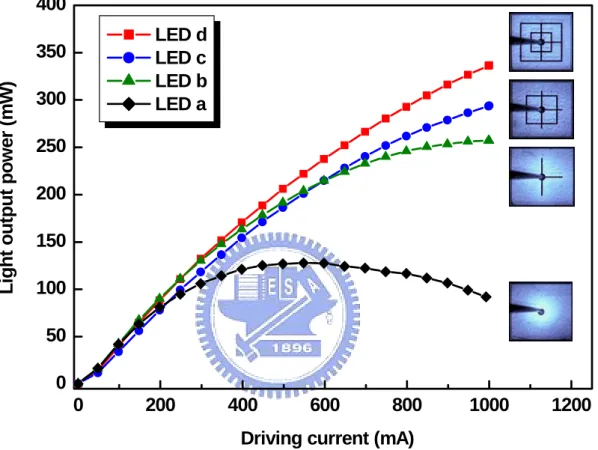
The L-I characteristics of the LEDs with four different n-electrode patterns under cw operation are shown in Fig. 3.12. The insets show the micrographic top view of the four LEDs driven at 100 mA in the sequence LED d, LED c, LED b, and LED a from top to bottom. The output power measurement was performed from the upper side of the chip using a large-area Si photodiode placed 5 mm above the samples. The light output power of the LEDs showed a linear increase as the driving current was increased to 250 mA. The light output power of the four LEDs is also approximately equal when the driving current was below 250 mA. The injection current is supposed to spread uniformly over the mesas on the four LEDs, which results in equal light output power when the driving current was below 250 mA. As the driving current was
increased above 250 mA, the light output power of LED a began started to saturate and decrease due to the carrier overflow effect and the thermal effect caused by the high current density distributed around the circular electrode corresponding to the previous discussion for Fig. 3.9. In LED b, the output power saturation was also observed under a current injection level above 600 mA. LED d showed superior L-I characteristics compared with the other LEDs due to its well-designed electrode pattern for providing uniform current spreading as indicated in Fig. 3.10(d), which consequently reduced the thermal and carrier overflow effects caused by localized high injection current density. As the injection current was driven at 1000 mA, the light output power of LED d was 1.15, 1.30 and 3.15 times larger than that of LED c,
LED b and LED a, respectively. The different light output powers among the four
LEDs as the driving current increased to 1000 mA is caused by different current densities in the active region of each LED, which depend on the distribution of the injected current over the LEDs, resulting in carrier over flow and thermal effects at different levels and consequently different external quantum efficiencies [3.8]. The results indicate that the patterns of n-electrodes have a marked influence on the light output power.
Sapphire n-GaN MQWs
p-GaN
SiN SiN mask
SiN
SiN Bonding metals
(1) (2)
(3) (4)
(5) (6)
Figure 3.1 Schematic fabrication steps of the large emission-area GaN LEDs
(7) (8)
(9)
Figure 3.1 Schematic fabrication steps of the large emission-area GaN LEDs
on Cu substrate.
KrF: excimer laser
Graphite plate Mo screw
Stainless steel plate Mo nut
Pre-bonded sample
Figure 3.3 SEM image of the n-GaN surface after LLO process.
Table 3.1 Electrical and thermal properties for several materials used in this dissertation. (Ref. 3.2) Melting point (oC) Electrical Thermal expansion coeff. resistivity (µohm-cm) (10-6/oC) Young’s modulus (GPa) Thermal conductivity (W/m-K) Sapphire 2053 10 11-1016 (ohm-cm) 5.0 390 35 Aluminum 660.1 4.3 23.0 70 240 Copper 1083 1.7 16.6 130 400 Gold 1063 2.2 14.2 78 297 Molybdenum 2625 5.2 4.8 329 146 Nickel 1455 6.8 12.8 214 92 Platinum 1774 10.6 9.0 168 71 Graphite 3800 2.2 6 1060 990 Steel 1400 4.5 11.8 195 16
n-contact n-GaN p-GaN InGaN/GaN MQWs Cu substrate Bonding metals SiN passivation
Figure 3.5 SEM image of the LED on Cu substrate. GaN LED film
Figure 3.6 (a) L-I-V characteristics of the large-area-emission
GaN LEDs on Cu substrate under continuous-wave operation. (b) Electroluminescence of the LLO-LED under a driving current of 200 mA. 0 200 400 600 800 1000 0 1 2 3 4 5 6 7 8 0 50 100 150 200 250 300 Li ght out put pow e r (m W ) Vol tage ( V ) Current (mA) 380 400 420 440 460 480 500 520 540 0 50 100 150 200 250 300 FWHM=22 nm 456 nm In te n s ity (a rb . u n it ) Wavelength (nm) (a) (b)
0 100 200 300 400 500 600 700 0.0 0.2 0.4 0.6 0.8 1.0 1.2 Ls=400 μm E m issi on i n te ns it y ( a rb. uni t)
Distance from n-electrode edge (μm)
x=0
Figure 3.7 Normalized emission intensity as a function of the distance from
the electrode edge. Inset shows the micrograph of the optical emission from the LED driven at 200 mA.
LED a LED b LED c LED d
Length of cross: 700 μm
Square width: 520 μm Length of cross: 700 μm
Square width: 350 & 700 μm Cross width: 700 μm Diameter: 120 μm
* Circular diameter and linear linewidth are 120 mm and 20 mm, respectively in the four patterns.
Pattern Dimension Figure 3.8 The schematic diagrams top view of the LED devices with
four different n-electrode patterns.
0
100
200
300
400
500
600
0
2
4
6
8
10
12
14
16
Driving current (mA)
Li
ght
out
p
ut
pow
e
r (
a
rb
. uni
t)
0.01%
10%
CW
LED aFigure 3.9 L-I characteristics of LED a under cw and pulse operations
Cu substrate
(c) (d) (a) (b)
Figure 3.10 Light emission patterns and intensity distributions of the LEDs with