行政院國家科學委員會專題研究計畫 成果報告
嵌入式 DRAM 測試方法
研究成果報告(精簡版)
計 畫 類 別 : 個別型
計 畫 編 號 : NSC 98-2221-E-009-132-
執 行 期 間 : 98 年 08 月 01 日至 99 年 07 月 31 日
執 行 單 位 : 國立交通大學電子工程學系及電子研究所
計 畫 主 持 人 : 趙家佐
計畫參與人員: 碩士班研究生-兼任助理人員:楊皓宇
碩士班研究生-兼任助理人員:陳弘昕
碩士班研究生-兼任助理人員:&;#20931;偉勝
碩士班研究生-兼任助理人員:陳擴安
碩士班研究生-兼任助理人員:郭淳仁
碩士班研究生-兼任助理人員:徐浩文
碩士班研究生-兼任助理人員:王易民
碩士班研究生-兼任助理人員:黃欽遠
碩士班研究生-兼任助理人員:張玟翔
碩士班研究生-兼任助理人員:張智為
碩士班研究生-兼任助理人員:曾遵銘
博士班研究生-兼任助理人員:穆思邦
博士班研究生-兼任助理人員:秦敬雨
博士班研究生-兼任助理人員:林政偉
報 告 附 件 : 出席國際會議研究心得報告及發表論文
處 理 方 式 : 本計畫可公開查詢
行政院國家科學委員會補助專題研究計畫成果報告
※※※※※※※※※※※※※※※※※※※※※※※※※※※
※ 嵌入式 DRAM 測試方法 ※
※※※※※※※※※※※※※※※※※※※※※※※※※※※
計畫類別:個別型計畫 □整合型計畫
計畫編號:NSC98-2221-E-9-132
執行期間: 98 年 8 月 1 日至 99 年 7 月 31 日
計畫主持人:趙家佐
共同主持人:
計畫參與人員:張智為 楊皓宇 陳弘昕 涂偉勝 陳擴安 郭淳仁 曾遵銘
林政偉 黃欽遠 張玟翔 徐浩文 王易民 穆思邦 秦敬雨
執行單位:
交通大學電子工程系
中 華 民 國 99 年 10 月 20 日
嵌入式 DRAM 測試方法
“Testing Methodology of Embedded DRAMs”
計畫編號:
NSC98-2221-E-9-132
執行期間:98 年 8 月 1 日 至 99 年 7 月 31 日
主持人:趙家佐 交通大學電子工程系助理教授
一、中文摘要 關鍵詞:嵌入式 DRAM;記憶體測試;資料維持測試; 瑕疵程度;可靠度測試; 在系統晶片的時代,我們須要有效率且經濟的嵌 入式記憶體,研究人員嘗試著將獨立 DRAM 的優點,帶 進系統晶片中。於是,過去的十年當中,許多研究資 源已經投入到嵌入式 DRAM(eDRAM)的領域,嘗試著將 eDRAM 對於邏輯製程來說的額外製程負擔降低。然而, 現有的文獻裡面,幾乎沒有研究在討論 eDRAM 的測試, 然而傳統獨立式 DRAM 的測試,是沒有辦法直接用在 eDRAM 測試上的。
既然 eDRAM 使用了 DRAM 的記憶體單元以及 SRAM 的介面,在本計畫當中,我們首先比較 eDRAM 測試, 與獨立式 DRAM 測試以及 SRAM 測試的不同。接著我們 整理出在 eDRAM 測試中所需要特別注意的錯誤模型, 以及可以測到這些錯誤模型所需的測試圖案。本計畫 的主要目標有二:(一) 研發出一最短的 eDRAM 測試 演算法;(二)研發出如何有效利用提升溫度,達到 降低資料延遲測試在 eSRAM 測試中的時間。 英文摘要
Key words: embedded DRAM, memory testing, data-retention test, defect level, reliability testing
With the strong need to an effective and economic embedded-memory core in the SoC era, researchers attempt to carry commodity DRAM's advantages from a commodity memory into a SoC. In the past decade, a lot research effort has been put into the area of the embedded-DRAM (eDRAM) technologies to reduce eDRAM's process adders to the CMOS process. However, few previous research works have discussed the testing strategies used for eDRAMs, which cannot be directly carried from the testing of commodity DRAMs.
In this project, we first compare the eDRAM testing to the commodity-DRAM testing and SRAM testing since an eDRAM core utilizes the DRAM cells with the SRAM interface. Then, we list the fault models which should be
specially considered in the eDRAM testing and find out the corresponding test sequence for each fault model. The main objectives of this project include (1) develop a minimal test algorithm for eDRAM testing, (2) develop an effective scheme to shorten the retention-test time in eDRAM testing based on increasing the temperature.
二、計畫緣由、目的、研究方法與實驗結果
1. INTRODUCTION
Due to the advantages of high density, structure simplicity, low-power consumption, and low cost, DRAM has been the mainstream of the commodity-memory market since its invention by Dr. Dennard [1]. With the continually growing need to an effective and economic embedded-memory core in the SoC era, researchers attempt to carry DRAM's advantages from a commodity memory into a SoC. In the past decade, a lot research effort has been put into the embedded-DRAM (eDRAM) technologies, such as deep-trench capacitor with bottle etch [2], planar capacitor [3] [4], shallow trench capacitor [4], and metal-insulator-metal (MIM) capacitor [3] [5], to reduce the process adders to the CMOS process, where the eDRAM is embedded in. The eDRAM technologies are now available in the IC-foundry industry [6][7] and its applications include the products of networking, multimedia handheld devices, gaming consoles, high definition television, and so forth.
The classical DRAM testing contains two main steps: the functional test and the retention test. In the functional test, each functionality of DRAM cells and DRAM's peripheral circuitry are verified. In the retention test, we check whether the data retention time, which is in the order of milliseconds, of each DRAM cell can meet its specification. An industrial test set for DRAM's functional test requires a series of different test algorithms to ensure its complete functionality and coverage [16]. Those algorithms include checkerboard, address complement, March, row/column disturb,
self-refresh, XMOVI, butterfly, etc. Applying all of the above test algorithms is time-consuming, thus commodity-DRAM testing heavily relies on the parallel testing capability provided by the memory testers to shorten the average test time of each DRAM chip. In fact, the architecture and functions of most current eDRAM cores use the interface of SRAM (1T-SRAM architecture), which consists of no address multiplexer and can auto- refresh, are simpler than commodity-DRAM. Therefore testing the functionality of eDRAM is simpler than that of commodity DRAM, and hence requires only a shorter test algorithm.
However, testing eDRAM is not completely the same as testing SRAM. Applying only the SRAM test algorithm for eDRAM testing is not sufficient due to the following reasons. First, testing eDRAM needs to consider word-line coupling faults and bit-line toggling faults, but testing SRAM does not. It is because the power/ground shielding technique is commonly used in modern SRAM designs to eliminate the signal disturbance between word-lines or bit-lines, but eDRAM does not have this mechanism. Second, the eDRAM has the functionality of auto-refresh and self-refresh but SRAM does not. Similar to DRAM, eDRAM need to test the retention time, which takes a significant portion of the overall eDRAM test time.
The specification of eDRAM's data-retention time is a constant. As a result, the ratio of this retention test time over the eDRAM test time increases when the clock frequency of the eDRAM increases. It implies that the retention-test time may dominate the eDRAM test time for high-performance eDRAM designs. The data- retention time of an eDRAM cell depends on the leakage current of the switch transistor in the cell, which is sensitive to the temperature [17][18]. Therefore, by properly increasing the test temperature, the retention test time can be significantly reduced.
In this project, we would like to share the
experience obtained from testing an industrial eDRAM core. We first discuss the test algorithms used for the eDRAM testing and compare the corresponding yields of different test algorithms through wafer-test results. We then analyze the test time of eDRAM retention test and its ratio to total eDRAM test time. Next, we study the leakage mechanisms of a switch transistor and theoretically compute the leakage-charge equivalence between different temperatures. Based on this leakage-charge equivalence, we can obtain the equivalent retention time used for retention test at different temperatures. We also report the test-time reduction by increasing tester's temperature and validate the equivalent retention-fault coverage through wafer-test results. All reported wafer-test results are collected from 1-lot test wafers.
2. OVERVIEW OF EMBEDDED DRAM
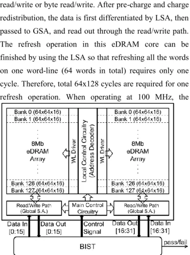
Figure 1 shows the block diagram of the 16Mb eDRAM core on our test chips. We will use this eDRAM core as the target instance throughout the rest of this project. This eDRAM core utilizes a 65nm low-leakage logic process. The size of the eDRAM core is around 4 mm2, which contains two symmetric eDRAM arrays with
8Mb data on each. Each array contains 128 banks, and each bank contains 64 word-lines and its own local sense amplifier (LSA). Each word-line on each array is connected to 64 half-words, and the data-width of each half-word is 16 bits. When a word is accessed, its first 16 bits are contributed from the first eDRAM array, and its last 16 bits are from the second array. Note that the layout topology of the eDRAM array utilizes the distributed folding scheme, where the ith bit of the jth word is adjacent to the ith bit of the (j+1)th word, not the (i+1)th bit of the original jth word. Between the two eDRAM arrays is the address decoder including word-line drivers. The control circuit (CTL) and global sense amplifier (GSA) are on the bottom of the eDRAM core.
The CTL controls all operations of eDRAM, including read, write, self-refresh, auto-refresh, and any application-dependent operation such as burst-mode read/write or byte read/write. After pre-charge and charge redistribution, the data is first differentiated by LSA, then passed to GSA, and read out through the read/write path. The refresh operation in this eDRAM core can be finished by using the LSA so that refreshing all the words on one word-line (64 words in total) requires only one cycle. Therefore, total 64x128 cycles are required for one refresh operation. When operating at 100 MHz, the
Fig. 1. Embedded-DRAM architecture.
bandwidth of this eDRAM core is 3.125 Gb/s (32 bits x 100 MHz).
During the eDRAM testing, the data background written into or read from the memory core should represent cell's physical value instead of its logical value. Therefore, when designing the BIST circuitry, we should consider the physical layout of the word-oriented eDRAM array [19]. The technique of address and data scrambling is commonly used in current memory designs, which can optimize memory's lay-out geometry, address decoder, cell area, performance, yield, and I/O pin compatibility [19]. The forms of scrambling include folding, address decoder scrambling, contact and well sharing, and bit-line twisting [19].
Figure 2 shows an exemplary scrambling used in
current popular eDRAM designs, where the ordering of word-lines in this example are arranged according to the least significant bits of the address. With an SRAM interface, eDRAM utilizes both bit-lines and bit-line-bars to distinguish the data value stored in an eDRAM cell, but a cell's data is only connected to either one of the corresponding bit-line and bit-line-bar. In this example, each word-line connects to two 4-bit words. The first word on a word line uses the 0th, 2nd, 4th, and 6th pairs of the bit-line and bit-line-bar, and the second word uses the 1st, 3rd, 5th, and 7th pairs. By proper arrangement, half of eDRAM cells are connected to bit-line, and the other half to the bit-line-bar. This balances the capacitor of the data-lines and improves the efficiency of eDRAM. As a result, the physical value of those cells connected to a bit-line-bar is inverse to their logical value. The bit-line twisting shown in the middle of Figure 2 can reduce the coupling capacitance between the bit-line of a cell and the bit-line-bar of the next cell [19]. Each bit-line twist for a given column reverses the physical-value/logical-value relation of the cells below that twist.
Fig. 2. An exemplary array scrambling. 3. THE EDRAM TEST APPROACH
3.1. Current SRAM Test Approach
In this section, we use the March C- algorithm as the basic skeleton of our eDRAM-testing algorithm. March C-algorithm is currently the most widely used test
algorithm for SRAM in industry, which can detect stuck-at faults (SAFs), transition faults (TFs), address decoder faults (AFs), inversion coupling faults (CFins), idempotent coupling faults (CFids), and state coupling faults (CFst) [1]. Below shows the element sequence of the March C- algorithm. The complexity of the March C- algorithm is 10N, where N is the density of the array. March C- (10N):
{⇑ (wa);⇑(ra,wb);⇑(rb,wa);⇓(ra,wb);⇓(rb,wa); ⇓ (ra)}
The notations are defined as follows. ⇑: address increase ⇓: address decrease a: data background b: complement background r: read w: write
3.2. Embedded-DRAM Test Strategies
Even though the interface of our eDRAM is the same as that of SRAM, applying only the SRAM test algorithm for eDRAM testing is not sufficient. Therefore, on top of this March C- algorithm, we need to add more elements to cover the faults which may not be considered in current SRAM testing but should be considered in the eDRAM testing, such as data-retention faults, word-line coupling faults, bit-line toggling faults, and stuck-open faults. We also need to test the functionality which eDRAM has but SRAM does not, such as auto-refresh and self-refresh. In the following subsections, we provide the corresponding test strategy for each of the above uncovered faults and functions in the March C- algorithm.
3.3. Proposed Embedded-DRAM Test Approach
In this section, we summarize the test strategies discussed in Section III-B to form the final test approach for an eDRAM core. This test approach applies an X-direction extended March C- algorithm with solid data-background as well as a Y-direction MATS algorithm with checkerboard data-background. Also, we
test the self-refresh operation in the extended March C- algorithm and the retention faults in the MATS algorithm. The auto-refresh is always on in both algorithms. The detail steps of the March C- and MATS algorithms are described as follows.
X-direction Extended March C- with solid background (11N):{⇑(wa);⇑(ra,wb,rb);(SR);⇑(rb,wa);⇓(ra,wb); ⇓(rb,wa); (SR);⇓ (ra)}
Y-direction MATS with checkerboard background (4N): {⇑ (wa);SR;del;⇑(ra,wb);SR;del;⇓(rb)}
SR: self-refresh.
del: delay element which stops for the period of the retention time defined in the specification.
The above X-direction extended March C- algorithm covers the stuck-open faults by the element (ra,wb,rb). It also tests the functionality of self-refresh and auto-refresh. The above Y-direction MATS algorithm tests the word-line-coupling faults by the Y-direction elements and checkerboard data-background. It also tests the retention faults by inserting the sequence of SR and del twice. The bit-line-toggling faults are covered by the solid-background operations in the extended March C- algorithm and the checkerboard-background operations in the Y-direction MATS algorithm.
From coverage's point of view, the two self-refresh operations in the extended March C- algorithm seem redundant since two self-refresh operations are also performed in the MATS algorithm for the retention test. However, we keep the first two self-refresh operations in our first tape-out to differentiate the detection of self-retention faults from that of the data-retention faults. These two self-refresh operations in the extended March C- algorithm can be further removed to speed up the test time if the diagnosis requirement is low.
3.4. Experimental Results
We apply the test set of the following three test approaches individually to the same eDRAM cores on
1-lot wafers through external testers, not BIST circuitry. 1. The proposed test approach
2. X-direction March C- with solid background plus Y-direction MATS with CHK background
3. X-direction March C+ with solid background plus Y-direction MATS with CHK background
The difference between proposed approach and the others is on their March algorithms in use. Approach 2 uses the basic March algorithm described in Section III-A and approach 3 uses the default March algorithm generated by a commercial memory-BIST tool, Memory
BIST Architecture [21]. Note that we turn off the
retention test in this experiment to save its test time. The experimental results containing the retention test will be discussed later in the Section IV.
Table I lists the yield of the above three test approaches. Our proposed approach and Approach 3 result in the same yield while the Approach 2 results in a higher yield. This result implies that only applying March C- may miss certain faults and lead to higher test escape. The proposed approach can achieve the same level of fault coverage with Approach 3. However, the proposed approach only requires a 11N extended March C- algorithm but Approach 3 requires a 14N March C+ algorithm. This result shows that the general SRAM algorithm, March C- (10N), cannot provide sufficient fault coverage, and the default March algorithm generated by a commercial tool, March C+ (14N), is redundant in our eDRAM testing.
TABLE I
3.5. Test Time Analysis for Proposed Test Approach
The total test time of the proposed test approach (Ttest) is the summation of the test time on retention test
(TRT ), read/write operations (TR/W ), self-refresh (TSR),
and auto-refresh (TAR). T test = T RT + T R/W + T SR + T AR (1) where T RT = 2 × T del (2) T R/W = N WORDS × N R/W × T CYCLE (3) T SR = N WL × N SR × T CYCLE (4) T AR = N WL × N AR × T CYCLE (5)
T del: time of one (del) element
T CYCLE: cycle time
N WORDS: number of words
N R/W: number of reads and writes
N WL: number of word-lines
N SR: number of self-refreshes
N AR: number of total auto-refreshes
Tdel is equal to the retention-time specification, and
NAR is equal to the runtime divide by the specified
retention time .
TABLE II
Table II lists the test time spent in each component of the proposed approach, given a 50MHz clock frequency and a 16ms retention-time specification. In this case, the ratio o f retention-test time to total test time is 17.4%.
4. REDUCING RETENTION-TEST TIME BY INCREASING TEMPERATURE
For an eDRAM cell, its data-retention time is determined by the leakage of its switch transistor, which increases along with the increase of the temperature. In the eDRAM testing, we attempt to raise the temperature to increase transistor's leakage current, which shortens the data-retention time of a cell. Therefore, at a higher temperature, the delay element used for retention test can be specified shorter since a retention fault can be detected within a shorter period of time than that at the original reference temperature. However, if the new specified retention time is too low, some retention faults may be able to escape, resulting in a higher defect level. On the contrary, if it is too high, the retention time of an eDRAM cell is over-tested, resulting in a yield lost.
In order to specify an appropriate retention time for the delay element at a higher temperature, we need to calculate the time at a given temperature during that the leakage of a switch transistor is equivalent to the leakage during the specified retention time at the reference temperature, which is defined as 85 oC in our
specification. This time is defined as the equivalent
retention time for a given temperature, which implies that
a eDRAM cell loses its data after the specified retention time at 85oC if and only if this cell will lose its data after
the equivalent retention time at the given temperature.
4.1. Leakage Mechanisms
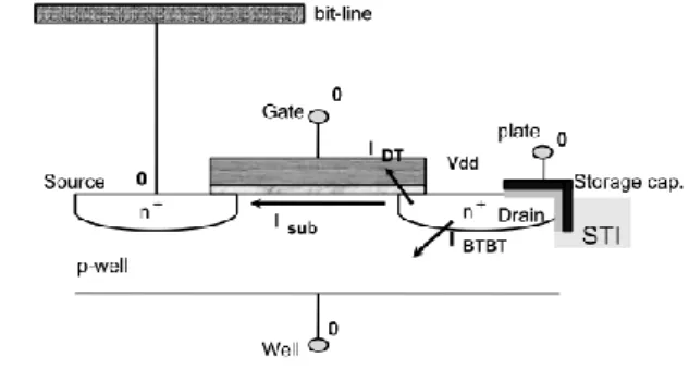
The leakage mechanisms of a deep-sub-micron transistor include reverse-bias pn junction leakage, subthreshold leak-age, oxide tunneling current, gate current due to hot-carrier injection, gate-induced drain leakage (GIDL), and channel punchthrough current [18]. Among these six leakage mechanisms, the reverse-bias junction Band-To-Band-Tunneling (BTBT) leakage, subthreshold leakage, and direct tunneling current are the main leakage sources in current advanced process technologies [17]. Figure 3 illustrates these three main leakage sources in the cross-section view of a cell in our eDRAM.
Fig. 3. Main leakage sources of a eDRAM cell.
Note that this leakage is actually a function of temperature. The following subsection discusses those temperature-dependent parameters in the above leakage equations. In addition, the leakage for the storage capacitor itself is small when using a high-k material and hence can be omitted in our analysis.
4.2. Temperature-Dependent Parameters in Leakage
Different leakage-current sources have different temperature dependence. In the following, we list the temperature-dependent parameters in above three leakage equations and discuss the magnitude of their dependency to the temperature θ.
1) Energy-band gap(Eg): The energy-band gap may be
narrowed by the increase of temperature within an order of 10−4θ2.
2) Junction electric field(E): The junction electric field
coupled with the doping concentration may be influenced by the temperature, but it is more dependent on the junction voltage.
3) Mobility(µ0): The increase of temperature results in the
reduction of mobility. The degradation of mobility is direct proportional to θ1.5.
4) Thermal voltage(VT): The thermal voltage is linearly
proportional to the temperature, which results in an exponential growth of the subthreshold leakage.
5) Threshold voltage(Vth): The increase of temperature
causes more carriers on the channel, which reduces the threshold voltage and hence increases the subthreshold leakage.
6) Barrier height(φox): The barrier height decreases when
temperature increases, which is proportional to 10−4θ. In summary, the direct-tunneling current is invariant to the temperature since the barrier height and potential drop across oxide are invariant to the temperature. The BTBT leakage may vary with the temperature but only in a small order. The subthreshold leakage increases significantly along with the increase of the temperature due to the decrease of Vth and the increase of thermal
voltage. Even though the direct-tunneling current and BTBT current are not sensitive to the temperature, both of them should still be considered in our leakage analysis since they contribute a significant portion of the total leakage at the normal temperature especially in advanced process technologies [17].
To calculate the equivalent retention time for a target temperature, we first calculate the total amount of charge (Qtotal) leaked from the storage capacitor during the
retention-time specification (Tref) at the reference
temperature (θref), i.e., 85
℃
.TABLE III
Table III lists the calculated equivalent retention time and its reduction ratio to the original specification-defined retention time associated with each given temperature. The retention-time specification (Tref )
is 16ms at the reference temperature (θref ) 85
℃
. As theresults shows, the retention-time reduction is close to 50% when raising the temperature to 105
℃
, and 65% when 120℃
, respectively. It implies that the retention- test time can be significantly reduced by raising the temperature.4.4. Experimental Results
In the following experiment, we apply our proposed test algorithm (described in Section III) on the eDRAM cores of 1-lot test wafers repeatedly with different retention-time specifications at different temperatures. In each time of the eDRAM testing, the delay element needs to match the retention-time specification. Table IV shows the corresponding yield for each retention-time specification and temperature. As the results show, the yield reaches 86.5% with 16ms retention time at 85
℃
. Also, the same yield is first-reached with 12ms retention time at 95℃
and 8ms retention time at 105℃
. This result implies that the eDRAM cells which hold their charge for 16ms at 85℃
can hold their charge for 12ms at 95℃
and for 8ms at 105℃
, respectively. This result approximately matches the calculated equivalent retention time listed in Table III, where the equivalent retention time for 95℃
and 105℃
is 11.55ms and 8.47ms, respectively.TABLE IV
Note that at a higher temperature, its equivalent retention time decreases, which results in more frequent auto-refresh operations. Fortunately, the time consumed by a refresh operation is short and does not affect test-time reduction too much. In addition, the temperature discussed here is for wafer testing. If we want to test the data retention after package, the temperature under consideration should be the temperature inside the package, not just tester's temperature. The temperature inside the package is higher than that outside the package. The table to map package's outside temperatures to its insides temperature can be obtained from the package providers.
三、結論
Even though an SRAM interface is used in an eDRAM core, testing an eDRAM core is more than just testing a SRAM core. In this thesis, we have discussed the testing strategies to detect the faults which may not be considered in SRAM testing but should be covered in eDRAM testing. We then proposed an eDRAM-testing approach to target those uncovered faults on top of a SRAM testing approach. Also, we analyze the relation between switch transistor's leakage and temperature. Based on that, we can theoretically calculate the equivalent retention time for different temperatures which can be adopted to reduce the retention-test time. The results were validated through the experiment of 1-lot test wafers.
1. A. J. van de Goor,”Testing Semiconductor Memories, Theory and Practice,” Gouda, The Netherlands: ComTex, 1998.
2. G. Wang, et al., ”A 0.127µm2 High Performance 65nm SOIBased embedded DRAM for on-Processor Applications,” International Electron Devices Meeting, 11-13 Dec. 2006, pp. 1-4.
3. E. Gerritsen, et al., ”Evolution of Materials Technology for Stacked-Capacitors in 65 nm Embedded-DRAM,” Solid-State Electronics, vol. 14, 2005, pp. 1767-1775.
4. M.-E. Jones, ”1T-SRAM-Q TM : Quad-Density Technology Reins in Spiraling Memory Requirements,” Mosys, Inc., Retrieved on 2007-10-06.
5. A. Berthelot, C. Caillat, V. Huard, S. Barnola, B. Boeck, H. Del-Puppo, N. Emonet, F. Lalanne, ”Highly Reliable TiN/ZrO 2 /TiN 3D Stacked Capacitors for 45 nm Embedded DRAM Technologies,” Proceeding of Solid-State Device Research Conference, Sept. 2006, pp. 343-346.
6. ”TSMC Embedded High Density Memory,” http://www.tsmc.com/. 7. ”0.13 Micron SoC Process Technology,” http://www.umc.com/. 8. ”A D&T Roundtable: Testing Mixed Logic and DRAM Chips,”
IEEE Design & Test of Computers, vol. 15, no. 2, Apr. June 1998, pp. 86-92.
9. C. Cheng, C.-T. Huang, J.-R. Huang, C.-W. Wu, C.-J. Wey, and M.-C. Tsai, ”BRAINS: A BIST compiler for embedded memories,” Proceedings of IEEE International Symposium on Defect and Fault Tolerance in VLSI Systems, Yamanashi, Oct. 2000, pp. 299-307. 10. J.-F. Li, R.-S. Tzeng and C.-W. Wu, ”Diagnostic Data Compression
Techniques for Embedded Memories with Built-In Self-Test,” J.Electronic Testing: Theory and Application, vol.18, no.4, Aug. 2002, pp. 515-527.
11. B. Nadeau-Dostie, A. Silburt, V.K. Agarwal, ”Serial Interfacing for Embedded Memory Testing,” IEEE Design & Test of Computers, vol. 7, no. 2, Apr 1990, pp. 52-63.
12. C.-T. Huang, J.-R. Huang, C.-F. Wu, C.-W. Wu, and T.-Y. Chang, ”A Programmable BIST Core for Embedded DRAM,” IEEE Design & Test of Computers, vol. 16, no. 1, Jan.-Mar. 1999, pp. 59-70.
13. J. E. Barth, et al., ”Embedded DRAM Design and Architecture for the IBM 0.11- µ m ASIC Offering,” IBM Journal of Research and
Development, vol. 46, no. 6, Nov. 2002, pp. 675-689.
14. S. Miyano, K. Sato, K. Numata, ”Universal Test Interface for Embedded-DRAM Testing,” IEEE Design & Test of Computers, vol. 16, no. 1, Jan.-Mar. 1999, pp. 59-70.
15. N. Watanabe, F. Morishita, Y. Taito, A. Yamazaki, T. Tanizaki, K. Dosaka, Y. Morooka, F. Igaue, K. Furue, Y. Nagura, T. Komoike, T. Morihara, A. Hachisuka, K. Arimoto, and H. Ozaki, ”An Embedded DRAM Hybrid Macro with Auto Signal Management and Enhanced- on-Chip Tester,” Proceedings of the IEEE International Solid-State Circuits Conference (ISSCC), Digest of Technical Papers, 2001, pp. 388-389.
16. A. J. van de Goor, ”An Industrial Evaluation of DRAM Tests,” IEEE Design & Test of Computers, vol. 21, no. 5, Sept.-Oct. 2004, pp. 430-440.
17. S. Mukhopadhyay, A. Raychowdhury, K. Roy, ”Accurate Estimation of Total Leakage in Nanometer-Scale Bulk CMOS Circuits Based on Device Geometry and Doping Profile,” IEEE Transaction Computer-Aided Design of Integrated Circuits and Systems, vol. 24, no. 3, March 2005, pp. 363-381.
18. K. Roy, S. Mukhopadhyay, and H. Mahmoodi- Meimand, ”Leakage Current Mechanisms and Leakage Reduction Techniques in Deep-Submicrometer CMOS Circuits,” Proceeding of the IEEE, vol. 91, No. 2, Feb. 2003, pp. 305-327.
19. A.J. van de Goor and I. Schanstra, ”Address and Data Scrambling: Causes and Impact on Memory Tests,” Proc. 1st IEEE Int'l Workshop on Electronic Design, Test and Application (DELTA 02), IEEE Press, 2002, pp. 128-136.
20. K.-L. Cheng, M.-F. Tsai, and C.-W. Wu, ”Neighborhood pattern-sensitive fault testing and diagnostics for random-access memories,” IEEE Trans. on Computer-Aided Design of Integrated Circuits and Systems, vol. 21, no. 11, Nov. 2002, pp. 1328-1336. 21. MBIST Architecht Reference Manual, V8, Mar. 2003.
22. Y. Taur and T. H. Ning, ”Fundamentals of Modern VLSI Devices,” New York: Cambridge Univ. Press, 1998.
行政院國家科學委員會補助專題研究計畫成果報告
※※※※※※※※※※※※※※※※※※※※※※※※※※※
※ 嵌入式 DRAM 測試方法 ※
※※※※※※※※※※※※※※※※※※※※※※※※※※※
計畫類別:個別型計畫 □整合型計畫
計畫編號:NSC98-2221-E-9-132
執行期間: 98 年 8 月 1 日至 99 年 7 月 31 日
計畫主持人:趙家佐
共同主持人:
計畫參與人員:張智為 楊皓宇 陳弘昕 涂偉勝 陳擴安 郭淳仁 曾遵銘
林政偉 黃欽遠 張玟翔 徐浩文 王易民 穆思邦 秦敬雨
執行單位:
交通大學電子工程系
中 華 民 國 99 年 10 月 20 日
嵌入式 DRAM 測試方法
“Testing Methodology of Embedded DRAMs”
計畫編號:
NSC98-2221-E-9-132
執行期間:98 年 8 月 1 日 至 99 年 7 月 31 日
主持人:趙家佐 交通大學電子工程系助理教授
一、中文摘要 關鍵詞:嵌入式 DRAM;記憶體測試;資料維持測試; 瑕疵程度;可靠度測試; 在系統晶片的時代,我們須要有效率且經濟的嵌 入式記憶體,研究人員嘗試著將獨立 DRAM 的優點,帶 進系統晶片中。於是,過去的十年當中,許多研究資 源已經投入到嵌入式 DRAM(eDRAM)的領域,嘗試著將 eDRAM 對於邏輯製程來說的額外製程負擔降低。然而, 現有的文獻裡面,幾乎沒有研究在討論 eDRAM 的測試, 然而傳統獨立式 DRAM 的測試,是沒有辦法直接用在 eDRAM 測試上的。
既然 eDRAM 使用了 DRAM 的記憶體單元以及 SRAM 的介面,在本計畫當中,我們首先比較 eDRAM 測試, 與獨立式 DRAM 測試以及 SRAM 測試的不同。接著我們 整理出在 eDRAM 測試中所需要特別注意的錯誤模型, 以及可以測到這些錯誤模型所需的測試圖案。本計畫 的主要目標有二:(一) 研發出一最短的 eDRAM 測試 演算法;(二)研發出如何有效利用提升溫度,達到 降低資料延遲測試在 eSRAM 測試中的時間。 英文摘要
Key words: embedded DRAM, memory testing, data-retention test, defect level, reliability testing
With the strong need to an effective and economic embedded-memory core in the SoC era, researchers attempt to carry commodity DRAM's advantages from a commodity memory into a SoC. In the past decade, a lot research effort has been put into the area of the embedded-DRAM (eDRAM) technologies to reduce eDRAM's process adders to the CMOS process. However, few previous research works have discussed the testing strategies used for eDRAMs, which cannot be directly carried from the testing of commodity DRAMs.
In this project, we first compare the eDRAM testing to the commodity-DRAM testing and SRAM testing since an eDRAM core utilizes the DRAM cells with the SRAM interface. Then, we list the fault models which should be
specially considered in the eDRAM testing and find out the corresponding test sequence for each fault model. The main objectives of this project include (1) develop a minimal test algorithm for eDRAM testing, (2) develop an effective scheme to shorten the retention-test time in eDRAM testing based on increasing the temperature.
二、計畫緣由、目的、研究方法與實驗結果
1. INTRODUCTION
Due to the advantages of high density, structure simplicity, low-power consumption, and low cost, DRAM has been the mainstream of the commodity-memory market since its invention by Dr. Dennard [1]. With the continually growing need to an effective and economic embedded-memory core in the SoC era, researchers attempt to carry DRAM's advantages from a commodity memory into a SoC. In the past decade, a lot research effort has been put into the embedded-DRAM (eDRAM) technologies, such as deep-trench capacitor with bottle etch [2], planar capacitor [3] [4], shallow trench capacitor [4], and metal-insulator-metal (MIM) capacitor [3] [5], to reduce the process adders to the CMOS process, where the eDRAM is embedded in. The eDRAM technologies are now available in the IC-foundry industry [6][7] and its applications include the products of networking, multimedia handheld devices, gaming consoles, high definition television, and so forth.
The classical DRAM testing contains two main steps: the functional test and the retention test. In the functional test, each functionality of DRAM cells and DRAM's peripheral circuitry are verified. In the retention test, we check whether the data retention time, which is in the order of milliseconds, of each DRAM cell can meet its specification. An industrial test set for DRAM's functional test requires a series of different test algorithms to ensure its complete functionality and coverage [16]. Those algorithms include checkerboard, address complement, March, row/column disturb,
self-refresh, XMOVI, butterfly, etc. Applying all of the above test algorithms is time-consuming, thus commodity-DRAM testing heavily relies on the parallel testing capability provided by the memory testers to shorten the average test time of each DRAM chip. In fact, the architecture and functions of most current eDRAM cores use the interface of SRAM (1T-SRAM architecture), which consists of no address multiplexer and can auto- refresh, are simpler than commodity-DRAM. Therefore testing the functionality of eDRAM is simpler than that of commodity DRAM, and hence requires only a shorter test algorithm.
However, testing eDRAM is not completely the same as testing SRAM. Applying only the SRAM test algorithm for eDRAM testing is not sufficient due to the following reasons. First, testing eDRAM needs to consider word-line coupling faults and bit-line toggling faults, but testing SRAM does not. It is because the power/ground shielding technique is commonly used in modern SRAM designs to eliminate the signal disturbance between word-lines or bit-lines, but eDRAM does not have this mechanism. Second, the eDRAM has the functionality of auto-refresh and self-refresh but SRAM does not. Similar to DRAM, eDRAM need to test the retention time, which takes a significant portion of the overall eDRAM test time.
The specification of eDRAM's data-retention time is a constant. As a result, the ratio of this retention test time over the eDRAM test time increases when the clock frequency of the eDRAM increases. It implies that the retention-test time may dominate the eDRAM test time for high-performance eDRAM designs. The data- retention time of an eDRAM cell depends on the leakage current of the switch transistor in the cell, which is sensitive to the temperature [17][18]. Therefore, by properly increasing the test temperature, the retention test time can be significantly reduced.
In this project, we would like to share the
experience obtained from testing an industrial eDRAM core. We first discuss the test algorithms used for the eDRAM testing and compare the corresponding yields of different test algorithms through wafer-test results. We then analyze the test time of eDRAM retention test and its ratio to total eDRAM test time. Next, we study the leakage mechanisms of a switch transistor and theoretically compute the leakage-charge equivalence between different temperatures. Based on this leakage-charge equivalence, we can obtain the equivalent retention time used for retention test at different temperatures. We also report the test-time reduction by increasing tester's temperature and validate the equivalent retention-fault coverage through wafer-test results. All reported wafer-test results are collected from 1-lot test wafers.
2. OVERVIEW OF EMBEDDED DRAM
Figure 1 shows the block diagram of the 16Mb eDRAM core on our test chips. We will use this eDRAM core as the target instance throughout the rest of this project. This eDRAM core utilizes a 65nm low-leakage logic process. The size of the eDRAM core is around 4 mm2, which contains two symmetric eDRAM arrays with
8Mb data on each. Each array contains 128 banks, and each bank contains 64 word-lines and its own local sense amplifier (LSA). Each word-line on each array is connected to 64 half-words, and the data-width of each half-word is 16 bits. When a word is accessed, its first 16 bits are contributed from the first eDRAM array, and its last 16 bits are from the second array. Note that the layout topology of the eDRAM array utilizes the distributed folding scheme, where the ith bit of the jth word is adjacent to the ith bit of the (j+1)th word, not the (i+1)th bit of the original jth word. Between the two eDRAM arrays is the address decoder including word-line drivers. The control circuit (CTL) and global sense amplifier (GSA) are on the bottom of the eDRAM core.
The CTL controls all operations of eDRAM, including read, write, self-refresh, auto-refresh, and any application-dependent operation such as burst-mode read/write or byte read/write. After pre-charge and charge redistribution, the data is first differentiated by LSA, then passed to GSA, and read out through the read/write path. The refresh operation in this eDRAM core can be finished by using the LSA so that refreshing all the words on one word-line (64 words in total) requires only one cycle. Therefore, total 64x128 cycles are required for one refresh operation. When operating at 100 MHz, the
Fig. 1. Embedded-DRAM architecture.
bandwidth of this eDRAM core is 3.125 Gb/s (32 bits x 100 MHz).
During the eDRAM testing, the data background written into or read from the memory core should represent cell's physical value instead of its logical value. Therefore, when designing the BIST circuitry, we should consider the physical layout of the word-oriented eDRAM array [19]. The technique of address and data scrambling is commonly used in current memory designs, which can optimize memory's lay-out geometry, address decoder, cell area, performance, yield, and I/O pin compatibility [19]. The forms of scrambling include folding, address decoder scrambling, contact and well sharing, and bit-line twisting [19].
Figure 2 shows an exemplary scrambling used in
current popular eDRAM designs, where the ordering of word-lines in this example are arranged according to the least significant bits of the address. With an SRAM interface, eDRAM utilizes both bit-lines and bit-line-bars to distinguish the data value stored in an eDRAM cell, but a cell's data is only connected to either one of the corresponding bit-line and bit-line-bar. In this example, each word-line connects to two 4-bit words. The first word on a word line uses the 0th, 2nd, 4th, and 6th pairs of the bit-line and bit-line-bar, and the second word uses the 1st, 3rd, 5th, and 7th pairs. By proper arrangement, half of eDRAM cells are connected to bit-line, and the other half to the bit-line-bar. This balances the capacitor of the data-lines and improves the efficiency of eDRAM. As a result, the physical value of those cells connected to a bit-line-bar is inverse to their logical value. The bit-line twisting shown in the middle of Figure 2 can reduce the coupling capacitance between the bit-line of a cell and the bit-line-bar of the next cell [19]. Each bit-line twist for a given column reverses the physical-value/logical-value relation of the cells below that twist.
Fig. 2. An exemplary array scrambling. 3. THE EDRAM TEST APPROACH
3.1. Current SRAM Test Approach
In this section, we use the March C- algorithm as the basic skeleton of our eDRAM-testing algorithm. March C-algorithm is currently the most widely used test
algorithm for SRAM in industry, which can detect stuck-at faults (SAFs), transition faults (TFs), address decoder faults (AFs), inversion coupling faults (CFins), idempotent coupling faults (CFids), and state coupling faults (CFst) [1]. Below shows the element sequence of the March C- algorithm. The complexity of the March C- algorithm is 10N, where N is the density of the array. March C- (10N):
{⇑ (wa);⇑(ra,wb);⇑(rb,wa);⇓(ra,wb);⇓(rb,wa); ⇓ (ra)}
The notations are defined as follows. ⇑: address increase ⇓: address decrease a: data background b: complement background r: read w: write
3.2. Embedded-DRAM Test Strategies
Even though the interface of our eDRAM is the same as that of SRAM, applying only the SRAM test algorithm for eDRAM testing is not sufficient. Therefore, on top of this March C- algorithm, we need to add more elements to cover the faults which may not be considered in current SRAM testing but should be considered in the eDRAM testing, such as data-retention faults, word-line coupling faults, bit-line toggling faults, and stuck-open faults. We also need to test the functionality which eDRAM has but SRAM does not, such as auto-refresh and self-refresh. In the following subsections, we provide the corresponding test strategy for each of the above uncovered faults and functions in the March C- algorithm.
3.3. Proposed Embedded-DRAM Test Approach
In this section, we summarize the test strategies discussed in Section III-B to form the final test approach for an eDRAM core. This test approach applies an X-direction extended March C- algorithm with solid data-background as well as a Y-direction MATS algorithm with checkerboard data-background. Also, we
test the self-refresh operation in the extended March C- algorithm and the retention faults in the MATS algorithm. The auto-refresh is always on in both algorithms. The detail steps of the March C- and MATS algorithms are described as follows.
X-direction Extended March C- with solid background (11N):{⇑(wa);⇑(ra,wb,rb);(SR);⇑(rb,wa);⇓(ra,wb); ⇓(rb,wa); (SR);⇓ (ra)}
Y-direction MATS with checkerboard background (4N): {⇑ (wa);SR;del;⇑(ra,wb);SR;del;⇓(rb)}
SR: self-refresh.
del: delay element which stops for the period of the retention time defined in the specification.
The above X-direction extended March C- algorithm covers the stuck-open faults by the element (ra,wb,rb). It also tests the functionality of self-refresh and auto-refresh. The above Y-direction MATS algorithm tests the word-line-coupling faults by the Y-direction elements and checkerboard data-background. It also tests the retention faults by inserting the sequence of SR and del twice. The bit-line-toggling faults are covered by the solid-background operations in the extended March C- algorithm and the checkerboard-background operations in the Y-direction MATS algorithm.
From coverage's point of view, the two self-refresh operations in the extended March C- algorithm seem redundant since two self-refresh operations are also performed in the MATS algorithm for the retention test. However, we keep the first two self-refresh operations in our first tape-out to differentiate the detection of self-retention faults from that of the data-retention faults. These two self-refresh operations in the extended March C- algorithm can be further removed to speed up the test time if the diagnosis requirement is low.
3.4. Experimental Results
We apply the test set of the following three test approaches individually to the same eDRAM cores on
1-lot wafers through external testers, not BIST circuitry. 1. The proposed test approach
2. X-direction March C- with solid background plus Y-direction MATS with CHK background
3. X-direction March C+ with solid background plus Y-direction MATS with CHK background
The difference between proposed approach and the others is on their March algorithms in use. Approach 2 uses the basic March algorithm described in Section III-A and approach 3 uses the default March algorithm generated by a commercial memory-BIST tool, Memory
BIST Architecture [21]. Note that we turn off the
retention test in this experiment to save its test time. The experimental results containing the retention test will be discussed later in the Section IV.
Table I lists the yield of the above three test approaches. Our proposed approach and Approach 3 result in the same yield while the Approach 2 results in a higher yield. This result implies that only applying March C- may miss certain faults and lead to higher test escape. The proposed approach can achieve the same level of fault coverage with Approach 3. However, the proposed approach only requires a 11N extended March C- algorithm but Approach 3 requires a 14N March C+ algorithm. This result shows that the general SRAM algorithm, March C- (10N), cannot provide sufficient fault coverage, and the default March algorithm generated by a commercial tool, March C+ (14N), is redundant in our eDRAM testing.
TABLE I
3.5. Test Time Analysis for Proposed Test Approach
The total test time of the proposed test approach (Ttest) is the summation of the test time on retention test
(TRT ), read/write operations (TR/W ), self-refresh (TSR),
and auto-refresh (TAR). T test = T RT + T R/W + T SR + T AR (1) where T RT = 2 × T del (2) T R/W = N WORDS × N R/W × T CYCLE (3) T SR = N WL × N SR × T CYCLE (4) T AR = N WL × N AR × T CYCLE (5)
T del: time of one (del) element
T CYCLE: cycle time
N WORDS: number of words
N R/W: number of reads and writes
N WL: number of word-lines
N SR: number of self-refreshes
N AR: number of total auto-refreshes
Tdel is equal to the retention-time specification, and
NAR is equal to the runtime divide by the specified
retention time .
TABLE II
Table II lists the test time spent in each component of the proposed approach, given a 50MHz clock frequency and a 16ms retention-time specification. In this case, the ratio o f retention-test time to total test time is 17.4%.
4. REDUCING RETENTION-TEST TIME BY INCREASING TEMPERATURE
For an eDRAM cell, its data-retention time is determined by the leakage of its switch transistor, which increases along with the increase of the temperature. In the eDRAM testing, we attempt to raise the temperature to increase transistor's leakage current, which shortens the data-retention time of a cell. Therefore, at a higher temperature, the delay element used for retention test can be specified shorter since a retention fault can be detected within a shorter period of time than that at the original reference temperature. However, if the new specified retention time is too low, some retention faults may be able to escape, resulting in a higher defect level. On the contrary, if it is too high, the retention time of an eDRAM cell is over-tested, resulting in a yield lost.
In order to specify an appropriate retention time for the delay element at a higher temperature, we need to calculate the time at a given temperature during that the leakage of a switch transistor is equivalent to the leakage during the specified retention time at the reference temperature, which is defined as 85 oC in our
specification. This time is defined as the equivalent
retention time for a given temperature, which implies that
a eDRAM cell loses its data after the specified retention time at 85oC if and only if this cell will lose its data after
the equivalent retention time at the given temperature.
4.1. Leakage Mechanisms
The leakage mechanisms of a deep-sub-micron transistor include reverse-bias pn junction leakage, subthreshold leak-age, oxide tunneling current, gate current due to hot-carrier injection, gate-induced drain leakage (GIDL), and channel punchthrough current [18]. Among these six leakage mechanisms, the reverse-bias junction Band-To-Band-Tunneling (BTBT) leakage, subthreshold leakage, and direct tunneling current are the main leakage sources in current advanced process technologies [17]. Figure 3 illustrates these three main leakage sources in the cross-section view of a cell in our eDRAM.
Fig. 3. Main leakage sources of a eDRAM cell.
Note that this leakage is actually a function of temperature. The following subsection discusses those temperature-dependent parameters in the above leakage equations. In addition, the leakage for the storage capacitor itself is small when using a high-k material and hence can be omitted in our analysis.
4.2. Temperature-Dependent Parameters in Leakage
Different leakage-current sources have different temperature dependence. In the following, we list the temperature-dependent parameters in above three leakage equations and discuss the magnitude of their dependency to the temperature θ.
1) Energy-band gap(Eg): The energy-band gap may be
narrowed by the increase of temperature within an order of 10−4θ2.
2) Junction electric field(E): The junction electric field
coupled with the doping concentration may be influenced by the temperature, but it is more dependent on the junction voltage.
3) Mobility(µ0): The increase of temperature results in the
reduction of mobility. The degradation of mobility is direct proportional to θ1.5.
4) Thermal voltage(VT): The thermal voltage is linearly
proportional to the temperature, which results in an exponential growth of the subthreshold leakage.
5) Threshold voltage(Vth): The increase of temperature
causes more carriers on the channel, which reduces the threshold voltage and hence increases the subthreshold leakage.
6) Barrier height(φox): The barrier height decreases when
temperature increases, which is proportional to 10−4θ. In summary, the direct-tunneling current is invariant to the temperature since the barrier height and potential drop across oxide are invariant to the temperature. The BTBT leakage may vary with the temperature but only in a small order. The subthreshold leakage increases significantly along with the increase of the temperature due to the decrease of Vth and the increase of thermal
voltage. Even though the direct-tunneling current and BTBT current are not sensitive to the temperature, both of them should still be considered in our leakage analysis since they contribute a significant portion of the total leakage at the normal temperature especially in advanced process technologies [17].
To calculate the equivalent retention time for a target temperature, we first calculate the total amount of charge (Qtotal) leaked from the storage capacitor during the
retention-time specification (Tref) at the reference
temperature (θref), i.e., 85
℃
.TABLE III
Table III lists the calculated equivalent retention time and its reduction ratio to the original specification-defined retention time associated with each given temperature. The retention-time specification (Tref )
is 16ms at the reference temperature (θref ) 85
℃
. As theresults shows, the retention-time reduction is close to 50% when raising the temperature to 105
℃
, and 65% when 120℃
, respectively. It implies that the retention- test time can be significantly reduced by raising the temperature.4.4. Experimental Results
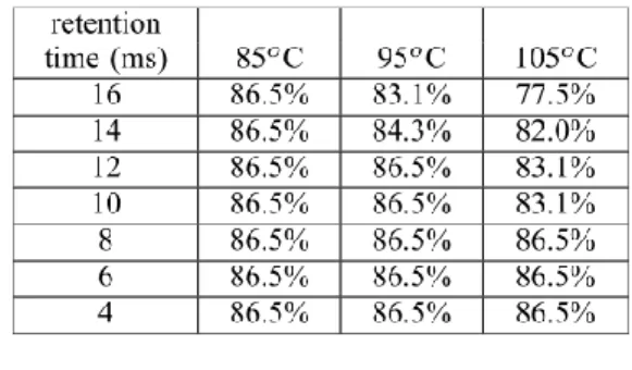
In the following experiment, we apply our proposed test algorithm (described in Section III) on the eDRAM cores of 1-lot test wafers repeatedly with different retention-time specifications at different temperatures. In each time of the eDRAM testing, the delay element needs to match the retention-time specification. Table IV shows the corresponding yield for each retention-time specification and temperature. As the results show, the yield reaches 86.5% with 16ms retention time at 85
℃
. Also, the same yield is first-reached with 12ms retention time at 95℃
and 8ms retention time at 105℃
. This result implies that the eDRAM cells which hold their charge for 16ms at 85℃
can hold their charge for 12ms at 95℃
and for 8ms at 105℃
, respectively. This result approximately matches the calculated equivalent retention time listed in Table III, where the equivalent retention time for 95℃
and 105℃
is 11.55ms and 8.47ms, respectively.TABLE IV
Note that at a higher temperature, its equivalent retention time decreases, which results in more frequent auto-refresh operations. Fortunately, the time consumed by a refresh operation is short and does not affect test-time reduction too much. In addition, the temperature discussed here is for wafer testing. If we want to test the data retention after package, the temperature under consideration should be the temperature inside the package, not just tester's temperature. The temperature inside the package is higher than that outside the package. The table to map package's outside temperatures to its insides temperature can be obtained from the package providers.
三、結論
Even though an SRAM interface is used in an eDRAM core, testing an eDRAM core is more than just testing a SRAM core. In this thesis, we have discussed the testing strategies to detect the faults which may not be considered in SRAM testing but should be covered in eDRAM testing. We then proposed an eDRAM-testing approach to target those uncovered faults on top of a SRAM testing approach. Also, we analyze the relation between switch transistor's leakage and temperature. Based on that, we can theoretically calculate the equivalent retention time for different temperatures which can be adopted to reduce the retention-test time. The results were validated through the experiment of 1-lot test wafers.
1. A. J. van de Goor,”Testing Semiconductor Memories, Theory and Practice,” Gouda, The Netherlands: ComTex, 1998.
2. G. Wang, et al., ”A 0.127µm2 High Performance 65nm SOIBased embedded DRAM for on-Processor Applications,” International Electron Devices Meeting, 11-13 Dec. 2006, pp. 1-4.
3. E. Gerritsen, et al., ”Evolution of Materials Technology for Stacked-Capacitors in 65 nm Embedded-DRAM,” Solid-State Electronics, vol. 14, 2005, pp. 1767-1775.
4. M.-E. Jones, ”1T-SRAM-Q TM : Quad-Density Technology Reins in Spiraling Memory Requirements,” Mosys, Inc., Retrieved on 2007-10-06.
5. A. Berthelot, C. Caillat, V. Huard, S. Barnola, B. Boeck, H. Del-Puppo, N. Emonet, F. Lalanne, ”Highly Reliable TiN/ZrO 2 /TiN 3D Stacked Capacitors for 45 nm Embedded DRAM Technologies,” Proceeding of Solid-State Device Research Conference, Sept. 2006, pp. 343-346.
6. ”TSMC Embedded High Density Memory,” http://www.tsmc.com/. 7. ”0.13 Micron SoC Process Technology,” http://www.umc.com/. 8. ”A D&T Roundtable: Testing Mixed Logic and DRAM Chips,”
IEEE Design & Test of Computers, vol. 15, no. 2, Apr. June 1998, pp. 86-92.
9. C. Cheng, C.-T. Huang, J.-R. Huang, C.-W. Wu, C.-J. Wey, and M.-C. Tsai, ”BRAINS: A BIST compiler for embedded memories,” Proceedings of IEEE International Symposium on Defect and Fault Tolerance in VLSI Systems, Yamanashi, Oct. 2000, pp. 299-307. 10. J.-F. Li, R.-S. Tzeng and C.-W. Wu, ”Diagnostic Data Compression
Techniques for Embedded Memories with Built-In Self-Test,” J.Electronic Testing: Theory and Application, vol.18, no.4, Aug. 2002, pp. 515-527.
11. B. Nadeau-Dostie, A. Silburt, V.K. Agarwal, ”Serial Interfacing for Embedded Memory Testing,” IEEE Design & Test of Computers, vol. 7, no. 2, Apr 1990, pp. 52-63.
12. C.-T. Huang, J.-R. Huang, C.-F. Wu, C.-W. Wu, and T.-Y. Chang, ”A Programmable BIST Core for Embedded DRAM,” IEEE Design & Test of Computers, vol. 16, no. 1, Jan.-Mar. 1999, pp. 59-70.
13. J. E. Barth, et al., ”Embedded DRAM Design and Architecture for the IBM 0.11- µ m ASIC Offering,” IBM Journal of Research and
Development, vol. 46, no. 6, Nov. 2002, pp. 675-689.
14. S. Miyano, K. Sato, K. Numata, ”Universal Test Interface for Embedded-DRAM Testing,” IEEE Design & Test of Computers, vol. 16, no. 1, Jan.-Mar. 1999, pp. 59-70.
15. N. Watanabe, F. Morishita, Y. Taito, A. Yamazaki, T. Tanizaki, K. Dosaka, Y. Morooka, F. Igaue, K. Furue, Y. Nagura, T. Komoike, T. Morihara, A. Hachisuka, K. Arimoto, and H. Ozaki, ”An Embedded DRAM Hybrid Macro with Auto Signal Management and Enhanced- on-Chip Tester,” Proceedings of the IEEE International Solid-State Circuits Conference (ISSCC), Digest of Technical Papers, 2001, pp. 388-389.
16. A. J. van de Goor, ”An Industrial Evaluation of DRAM Tests,” IEEE Design & Test of Computers, vol. 21, no. 5, Sept.-Oct. 2004, pp. 430-440.
17. S. Mukhopadhyay, A. Raychowdhury, K. Roy, ”Accurate Estimation of Total Leakage in Nanometer-Scale Bulk CMOS Circuits Based on Device Geometry and Doping Profile,” IEEE Transaction Computer-Aided Design of Integrated Circuits and Systems, vol. 24, no. 3, March 2005, pp. 363-381.
18. K. Roy, S. Mukhopadhyay, and H. Mahmoodi- Meimand, ”Leakage Current Mechanisms and Leakage Reduction Techniques in Deep-Submicrometer CMOS Circuits,” Proceeding of the IEEE, vol. 91, No. 2, Feb. 2003, pp. 305-327.
19. A.J. van de Goor and I. Schanstra, ”Address and Data Scrambling: Causes and Impact on Memory Tests,” Proc. 1st IEEE Int'l Workshop on Electronic Design, Test and Application (DELTA 02), IEEE Press, 2002, pp. 128-136.
20. K.-L. Cheng, M.-F. Tsai, and C.-W. Wu, ”Neighborhood pattern-sensitive fault testing and diagnostics for random-access memories,” IEEE Trans. on Computer-Aided Design of Integrated Circuits and Systems, vol. 21, no. 11, Nov. 2002, pp. 1328-1336. 21. MBIST Architecht Reference Manual, V8, Mar. 2003.
22. Y. Taur and T. H. Ning, ”Fundamentals of Modern VLSI Devices,” New York: Cambridge Univ. Press, 1998.