Performance improvement of pentacene-based organic thin-film transistor with HfO2 gate dielectrics treated by CF4 plasma
Kow-Ming Changa,b, Sung-Hung Huanga,*, Yi-Wen Tsenga
a Department of Electronics Engineering & Institute of Electronics, National Chiao Tung
University, 1001 Ta Hsueh Road, Hsinchu, Taiwan 30010, R.O.C.
b College of Electrical and Information Engineering, I-Shou University, Kaohsiung
County, Taiwan 84001, R.O.C.
Fluorine incorporation into the HfO2 gate dielectrics by post CF4
plasma treatment in an inductively coupled plasma chamber was proposed to improve gate leakage current and modify surface property for low-temperature fabrication. During the whole process, the temperature is controlled below 150 oC. The low-leakage HfO2
dielectric treated by CF4 plasma was characterized and then
utilized in pentacene-based OTFTs. After CF4 plasma treatment,
the gate leakage and field effect mobility were effectively improved. By integrating high-k HfO2 by CF4 plasma treatment
and HMDS evaporation treatment, a low operating voltage (-4V), low threshold voltage (-1.12V), a low subthreshold swing (266 mV/decade), a field-effect mobility (0.029cm2/Vs) and an on/off
current ratio (>104) were obtained. Introduction
Organic thin film transistors (OTFTs) have attracted considerable attention because they can potentially be developed into lightweight, flexible, and low-cost electronic device. In order to reduce operation voltage and improve performance, several high-k gate dielectrics were reported, such as Al2O3 (1), Ta2O5 (2), TiO2 (3) and HfO2 (4). Among
these dielectrics, HfO2 thin films were widely investigated as a potential high-k oxide in
replacement of SiO2 for ultra large scale integration (ULSI) technology due to high
dielectric constant and wide energy bandgap. In previous reports, HfO2 gate dielectric
treated by CF4 plasma can effectively reduce leakage current and hysteresis phenomenon
(5, 6). In addition, the electrical properties of OTFTs are highly determined between the gate dielectric and channel. The CFx also used to modify the interface to improve the electrical properties of OTFT (7).
Organic thin film transistors with low operation voltage and low process temperature are required for Flexible Electronics (8). Using high-k dielectrics can increase capacitance density which can reduce the threshold voltage and subthreshold swing (9). However, the high-k dielectrics which deposited at low temperature have more defects, so they usually need a high temperature annealing more than 300oC to effectively reduce leakage current. High-density inductively coupled plasma (ICP) sources are widely used in semiconductor fabrication processing. The inductively coupled plasma (ICP) chamber can independently control the plasma density as well as ion bombardment energy. In this work, fluorine incorporation into the HfO2 gate dielectrics by post CF4
plasma treatment at 150oC in an ICP chamber was proposed to improve not only gate leakage current but also surface property for low-temperature applications.
Experiment
First of all, a 500-nm SiO2 film was grown on silicon wafers by wet oxidation. The
Metal-insulator-Metal capacitors-(Ni/HfO2/Ni) were fabricated on SiO2/Si to analyze the
dielectric properties. The 50 nm-thick bottom nikel electrodes and 40 nm-thick HfO2 gate
dielectrics were deposited by electron beam evaporation. After the gate dielectric deposition, samples were treated by CF4 plasma in an inductively coupled plasma
chamber with pressure of 100 mTorr at 150 °C. The flow rate of CF4, ICP power and
process time are 100sccm, 500W, 90sec respectively. Next, top nikel electrodes were evaporated through a shadow mask (A= 4X10⁻⁵ cm2). The optimized parameter was used to fabricate OTFT. First, a 50-nm-thick nikel film was deposited and patterned through shadow mask to use as the gate electrode. Second, HfO2 gate dielectric was evaporated,
followed by CF4 plasma treatment. A control sample annealing for 1 hour at 150 °C in N2
without plasma treatment was also implemented. After CF4 treatment, HMDS is also
evaporated on gate dielectric surface to modify the surface property. Next, 80nm-thick pentacene (Aldrich Chemical Company) active layer was evaporated through a shadow mask on gate dielectric. This evaporation was performed at a deposition rate of 1Å/s at 70
oC, under a pressure of 3 × 10⁻⁶ torr. Finally, a 100 nm-thick gold was deposited onto the
pentacene to form a source/drain(S/D) contact. The devices had a channel length of 50μm and a width of 500μm. Figure 1 shows device structure of top contact OTFT.
X-ray photoelectron spectroscopy (XPS) was used to study the chemical bonding. The depth profile of fluorine incorporation was analyzed by the secondary ion mass spectroscopy (SIMS). The surface morphologies of dielectric and pentacene films were analyzed by atomic force microscopy (AFM). The high frequency (100 kHz) capacitance voltage (C-V) characteristics and current-voltage (I-V) curves were measured by Agilent 4156C and HP 4284, respectively.
Results and discussion
Since the plasma treatment maybe result in a rough surface which can degrade the performance, AFM is used to investigate on surface morphology without and with plasma treatment. Figure 2 shows the AFM surface images of HfO2 without treatment and with
CF4 plasma treatment. The rms roughness value is 0.596nm and 0.515nm respectively.
The result shows that the surface roughness is similar to the no treatment sample after plasma treatment.
675
680
685
690
695
700
Int
ensity(
a.u.)
Binding Energy
CF4 plasma treatment Without plasma treatmentF1s
Figure 2 AFM surface image of HfO2 (a) without plasma treatment (b) with CF4
plasma treatment
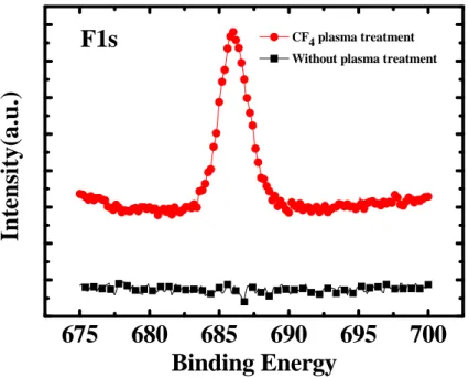
Figure 3 F 1s XPS spectrum for samples with and without CF4plasma treatment
F 1s XPS spectra in figure 3show that F is incorporated into HfO2 for samples with CF4 treatment. The peak located at ~685 eV corresponds to the F bonds in bulk HfO2 (10). From C1s XPS spectra shown in figure 4, C-F bond was observed at the surface after plasma treatment.
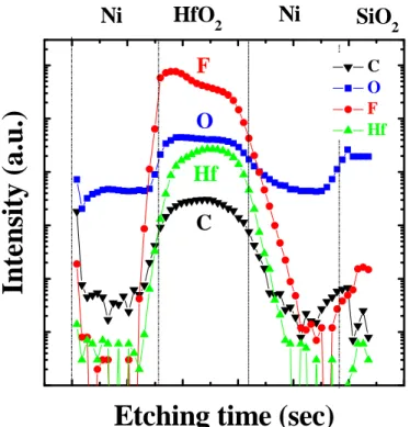
Figure 5 shows the depth profile of SIMS analysis of the HfO2 films with CF4 plasma
treatment. It can be seen that fluorine is incorporated into bulk HfO2 film, so that the
defects can effectively be passivated in bulk HfO2.
SiO
2
Ni
Intensity (a.u.)
Etching time (sec)
C O F HfC
Hf
O
F
Ni
HfO
2Figure 4 C 1s XPS spectrum for samples (a) without CF4 plasma treatment (b) with
CF4 plasma treatment (a) 282 284 286 288 290 292 C1s Inte nsi ty ( a .u.)
Binding energy (eV) No treatment C-H,C-C C=O 282 284 286 288 290 292 Inte nsi ty (a.u.)
Binding energy (eV)
CF4 plasma treatment
C1s C-H,C-C
C=O,C-F
(b)
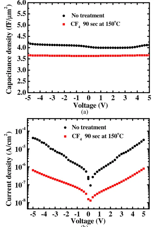
The C-V and J–V characteristics of MIM capacitors are shown in figures 6(a) and 6(b), respectively. It is observed that the capacitance slightly declines after plasma treatment. From C1s XPS data, it is deduced that C-F bonding results in a lower capacitance. As shown in figure 6(b), leakage current density of the gate dielectrics was significantly improved with CF4 plasma at 150 oC in an inductively coupled plasma
chamber, and gate dielectric leakage current was 3X10⁻⁶ A/cm2 at an electric field of 1MV/cm. The results show that fluorine atoms were incorporated into the HfO2
dielectrics to form Hf–F bonding by CF4 plasma, resulting in the reduction of gate
leakage current (6).
Figure 6 (a) C–V characteristics of Ni/HfO2/Ni capacitors (b) J–V characteristics of
Ni/HfO2/Ni capacitors with and without CF4 plasma.
-5 -4 -3 -2 -1
0
1
2
3
4
5
2.0
2.5
3.0
3.5
4.0
4.5
5.0
5.5
6.0
Capacitance densi
ty
(fF/
μ
m
2)
Voltage (V)
No treatment CF4 90 sec at 150oC(a)
-5 -4 -3 -2 -1 0
1
2
3
4
5
10
-810
-710
-610
-510
-4Curre
nt density
(A/cm
2)
Voltage (V)
No treatment
CF
490 sec at 150
oC
(b)
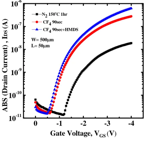
Figure 7 shows that the transfer characteristics of OTFTs with HfO2 gate dielectric
treated by annealing for 1 hour at 150 oC in N2 (control sample), CF4 plasma and CF4
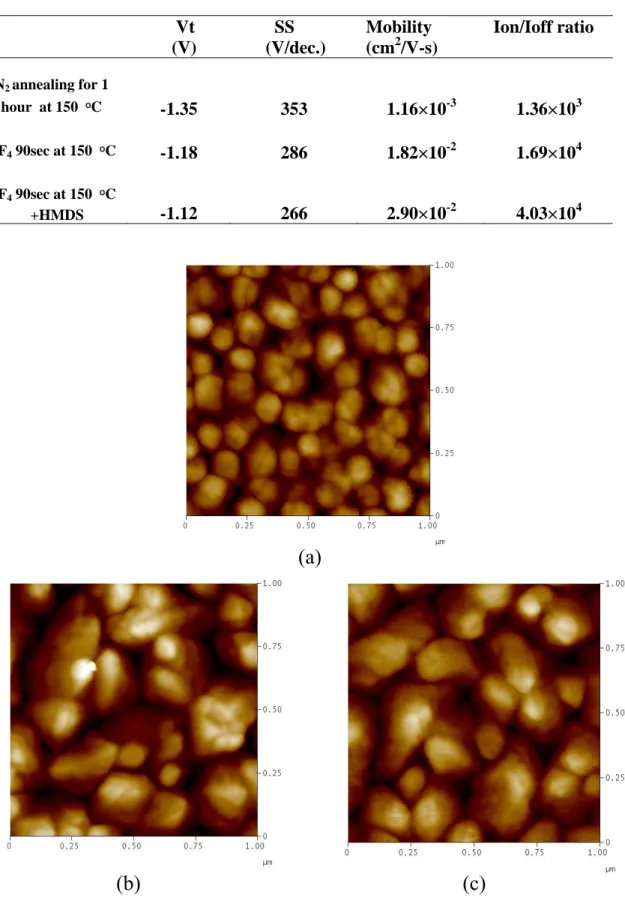
plasma followed by HMDS evaporation. Table 1 summarizes the electrical properties of subthreshold swing, on/off ratio, threshold voltage, and the mobility extracted by ID-VG and ID1/2 –VG plot. The mobility is enhanced after gate dielectric was treated by CF4
plasma and HMDS because of the improvement of carrier transport behavior on pentacene interface of channel/dielectric. Moreover, AFM surface images of pentacene were shown in figure 8. After CF4 plasma treatment, the grain size was larger resulting in
lager mobility than control sample. In Figure 9(a), ID-VD curve of control sample has more distortion due to high gate leakage current and lower mobility. After CF4 plasma
followed by HMDS treatment, the distortion is significantly improved since that F incorporation reduces the leakage current and improves surface property shown in figure 9(c). In figure 9(c), ID-VD shows slightly non-linear property at the low VDS region due
to the schottky barrier between pentacene and gold (11-13). In the previous reports, bottom contact structure shows more non-linear behavior than top contact (11, 12). It seems that our top contact structure presents a poor contact. The parasitic resistance in our experimental may result in a lower mobility.
0
-1
-2
-3
-4
10
-1110
-1010
-910
-810
-710
-6AB
S (
D
rain
Cu
rrent
) ,
I
DS(A)
Gate Voltage, V
GS(
V
)
N2 150oC 1hr CF4 90sec CF4 90sec+HMDS W= 500μm L= 50μmFigure 7 The transfer characteristics of OTFTs with HfO2 gate dielectric
treated by annealing for 1 hour at 150 oC in N2, CF4 plasma 90 sec at 150 oC,
TABLE I. Vt (V) SS (V/dec.) Mobility (cm2/V-s) Ion/Ioff ratio N2 annealing for 1 hour at 150 oC -1.35 353 1.16×10⁻³ 1.36×10³ CF4 90sec at 150 oC -1.18 286 1.82×10⁻² 1.69×10⁴ CF4 90sec at 150 oC +HMDS -1.12 266 2.90×10⁻² 4.03×10⁴
Figure 8 AFM pentacene deposited surface images after gate dielectric treated with (a) annealing for 1 hour at 150 oC in N2, (b) treated with CF4 plasma, and (c)
treated with CF4 plasma followed by HMDS evaporation treatment
(c)
(a)
Conclusion
In summary, a high-k HfO2 dielectric treated by CF4 plasma in an inductively
coupled plasma chamber was successfully integrated into pentacene-based OTFTs for low processing temperature. Fluorine incorporation into bulk HfO2 effectively repairs the
defect resulting in reduction of leakage current. The formation of C-F bonding at the gate dielectric surface modifies the surface properties resulting in a larger pentacene grain growth. Our pentacene-based OTFT by CF4 plasma and HMDS evaporation treatment
operated at -4V showing a low threshold voltage (-1.12V), a low subthreshold swing (266 mV/decade), a field-effect mobility (0.029 cm2/Vs) and an on/off current ratio (>104).
Figure 9 Output characteristics (ID–VD) of OTFTs for (a) annealing for 1 hour at 150
oC in N2 (b) CF4 plasma treated (c) CF4 plasma followed by HMDS evaporation
treatment 0 -1 -2 -3 -4 0.05 0.00 -0.05 -0.10 -0.15 -0.20 -0.25 VG= -1V VG= -2V VG= -3V VG= -4V W= 500μm L= 50μm Dr ain Curr ent , I DS ( μΑ ) Drain Voltage , VDS (V) VG= -1V VG= -2V VG= -3V VG= -4V 0 -1 -2 -3 -4 0.1 0.0 -0.1 -0.2 -0.3 -0.4 -0.5 -0.6 -0.7 -0.8 VG= -1V VG= -2V VG= -3V VG= -4V W= 500μm L= 50μm VG= -2V Dr ai n Cur re n t , I DS ( μΑ ) Drain Voltage , V DS (V) VG= -1V VG= -3V VG= -4V 0 -1 -2 -3 -4 0.20 0.15 0.10 0.05 0.00 -0.05 W= 500μm L= 50μm Dr ai n Curr ent , I DS ( μ A ) Drain Voltage , V DS (V) VG= -1V VG= -2V VG= -3V VG= -4V
(a)
(b)
(c)
Acknowledgments
The authors gratefully appreciate the technical and financial support from National Nano Device Laboratory of the National Science Council of the Republic of China under contract NDL98-C05SP-075. The authors would also like to thank the Nano Facility Center (NFC) of National Chiao-Tung University for providing process equipment.
References
1. X.-H. Zhang, B. Domercq, X. Wang, S. Yoo, T. Kondo, Z. L. Wang and B. Kippelen, Organic Electronics, 8, 718 (2007).
2. A. L. Deman, M. Erouel, D. Lallemand, M. Phaner-Goutorbe, P. Lang and J. Tardy, Journal of Non-Crystalline Solids, 354, 1598 (2008).
3. C. Jung, A. Maliakal, A. Sidorenko and T. Siegrist, Appl. Phys. Lett., 90, 062111 (2007).
4. J. Tardy, M. Erouel, A. L. Deman, A. Gagnaire, V. Teodorescu, M. G. Blanchin, B. Canut, A. Barau and M. Zaharescu, Microelectronics Reliability, 47, 372.
5. R. Xie, M. Yu, M. Y. Lai, L. Chan and C. Zhu, Appl. Phys. Lett., 92, 163505 (2008).
6. C. S. Lai, W. C. Wu, J. C. Wang and T. s. Chao, Appl. Phys. Lett., 86, 222905 (2005).
7. J. X. Tang, C. S. Lee, M. Y. Chan and S. T. Lee, Appl. Surf. Sci., 254, 7688 (2008). 8. K. D. Kim and C. K. Song, Appl. Phys. Lett., 88, 233508 (2006).
9. M. F. Chang, P. T. Lee, S. P. McAlister and A. Chin, Electron Device Letters, IEEE, 29, 215 (2008).
10. S. Kang-ill, R. Sreenivasan, P. C. McIntyre and K. C. Saraswat, Electron Device Letters, IEEE, 27, 821 (2006).
11. P. V. Necliudov, S. L. Rumyantsev, M. S. Shur, D. J. Gundlach and T. N. Jackson, 1/f noise in pentacene organic thin film transistors, p. 5395, AIP (2000).
12. O. Marinov, M. J. Deen and B. Iniguez, Circuits, Devices and Systems, IEE Proceedings -, 152, 189 (2005).
13. Z. Xie, M. S. A. Abdou, X. Lu, M. J. Deen, S. Holdcroft, Canadian Journal of Physics, Vol. 70(10-11), pp. 1171-1177, 1992