國
立
交
通
大
學
電子工程學系 電子研究所
博 士 論 文
應用於超寬頻及多通訊標準無線接收機之
互補式金氧半低雜訊前端電路
CMOS Low Noise Front-End for Ultra Wideband and
Multi-Standard Wireless Receiver
研 究 生:傅 昶 綜 Chang-Tsung Fu
指導教授:郭 建 男 Chien-Nan Kuo
應用於超寬頻及多通訊標準無線接收機之
互補式金氧半低雜訊前端電路
CMOS Low Noise Front-End for Ultra Wideband and
Multi-Standard Wireless Receiver
研
究
生: 傅昶綜
Student: Chang-Tsung Fu
指導教授: 郭建男 Advisor: Chien-Nan Kuo
國 立 交 通 大 學
電子工程學系 電子研究所
博 士 論 文
A Dissertation
Submitted to Department of Electronics Engineering and Institute of Electronics
College of Electrical and Computer Engineering National Chiao Tung University
in partial Fulfillment of the Requirements for the Degree of
Doctor of Philosophy in
Electronics Engineering
April 2009
Hsinchu, Taiwan, Republic of China
應用於超寬頻及多通訊標準無線接收機之
互補式金氧半低雜訊前端電路
研究生:傅昶綜 指導教授:郭建男 博士
國立交通大學 電子工程學系暨電子研究所
摘要
本篇論文主要探討達到寬頻同時雜訊及輸入阻抗匹配的低雜訊放大技術。在此針對 傳統的Y-參數雜訊分析方式進行改良,發展出較為準確的雜訊分析式,並依此定出設計 低雜訊放大器的最佳策略。在本論文中所提出之雙重電抗性迴授電路架構在配合LC 梯 狀阻抗匹配網路之後,可達成寬頻同時雜訊及輸入阻抗匹配的最佳低雜訊放大器之設計 條件。其中電感性部分迴授電路可以以變壓器迴授電路方式實現,大幅降低所需的晶片 面積。本技術應用在設計一個 3–11-GHz 超寬頻低雜訊放大器,以及一個 2.4–5.4-GHz 可程式帶限低雜訊放大器。在可程式帶限低雜訊放大器的應用中我們亦發展出電晶體及 電感之切換電路技術。前者提供電路性能的可程式特性,後者提供超寬可調頻率範圍並 有效維持一致的電路性能。 在低雜訊放大器之前,射頻收發切換器直接影響整體收發器的性能。在此發展出針 對 CMOS 特 性 的 電 路 設 計 技 術 以 提 高 切 換 器 的 線 性 度 及 耐 受 度 。 所 設 計 出 的 4.9–6.0-GHz 收發切換器可達到+30dBm 線性度以及低於 1-dB 的損耗。CMOS Low Noise Front-End Circuit for Ultra Wideband and
Multi-Standard Wireless Receiver
Student: Chang-Tsung Fu
Advisor: Chien-Nan Kuo
Department of Electronics Engineering
and Institute of Electronics
National Chiao-Tung University
Abstract
The technique of low noise amplification with broadband simultaneous noise and impedance matching (BSNIM) was developed. The conventional noise theory for MOSFET devices is revised to be more accurate. Strategies are addressed how to achieve low noise amplifier design. A dual reactive feedback topology along with an LC ladder matching network was proposed for BSNIM realization. The inductive feedback was implemented with a transformer feedback to reduce the circuit form factor. This technique was utilized to develop a 3–11-GHz ultra-wideband (UWB) LNA and a 2.4–5.4-GHz reconfigurable band-selection LNA. In the latter work the techniques of transistor switching and shunt inductor switching were developed. The transistor switching provides reconfiguration of performance including gain, linearity, and power consumption. The inductor switching provides a wide frequency tuning range while the voltage gain is consistent within the tuning range.
An RF T/R switch in front of LNA directly affects transceiver performance. Circuit design techniques were developed specifically for CMOS process to overcome the shortcoming of MOSFET when handling high power. In this thesis a 4.9–6.0-GHz T/R switch is demonstrated with sub-dB insertion loss and >30dBm power handling capability.
Acknowledgement
The author would like to express his greatest thanks to the two advisors in his Master and PhD programs in National Chiao Tung University (NCTU), Dr. Jieh-Tsorng Wu and Dr. Chien-Nan Kuo. Dr. Wu is an expert on analog circuit design and has a high standard on his student’s research quality and innovation. The author feels a great honor to inherit the strict research style from him. The analog circuit design techniques and those insight taught or advised by Dr. Wu also became the sound foundation of the author’s research.
In 2003, at Dr. Wu’s suggestion the author joined Dr. Kuo’s research group and assisted Dr. Kuo to administrate Ding-Hsiun High Frequency Laboratory. Since then, Dr. Kuo has been not only an advisor but also the best mentor and friend to the author. He provided a complete training, technical and non-technical, trying to make the author a qualified PhD. As an innovative research is typically full of risk and uncertainty, Dr. Kuo’s advices and encouragements strongly backed the author moving forward. As the result of his thoughtful guidance, the author has had the preliminary capability to execute a quality research independently from stem to stern. In 2006 Dr. Kuo encouraged the author to go abroad experiencing an internship in Intel Corp., Oregon, USA. To the author it has been the highest privilege having the chance to do research with the smartest engineers in the world. The author would like to express million of thanks to Dr. Kuo for all his considerate advises and those critically important favors in his PhD program.
The author would like to thank the committee members attending his thesis examination, Professor Ching-Kuang Tzuang and Professor Liang-Hung Lu from National Taiwan University (NTU), Professor Y. J. Chan from ITRI, Professor Shyh-Jong Chung and Professor Chin-Chun Meng from Department of Communication Engineering, NCTU, Professor
Shuo-Hung Hsu from National Tsing Hua University (NTHU), Professor Robert Hu from Department of Electronic Engineering, NCTU. Their insightful opinions and discussions make this dissertation more complete. Especially thanks Professor Tzuang for all his warm regards and thoughtful advices since the author was an undergraduate student. The author would like to thanks Professor Robert Hu exclusively for his dissertation, which gave the important inspiration on the idea of the dual reactive feedback circuit for BSNIM in chapter 2.
The author also would like to thank all the professors and students he had worked with in NCTU. Thanks so much for all the nice helps and discussions. Without you the author cannot have such a great experience in his PhD program.
The author would like to express his full thanks to his beloved parents and brother. Their greatest love supports the author among every second. Because of them, the author always feels confident and courageous toward any kind of challenges.
An exclusive thank is for Dr. Stewart S. Taylor in Intel Corp. for the invaluable discussion and advice. It’s amazing that Dr. Taylor and the author coincidently have similar results on noise analysis with different approaches. This adds confidence of the author on those very different equations from the conventional derivations in today’s literatures.
Finally, the author wishes this thesis could be helpful to all those students / researchers / engineers who may meet the similar problems.
Chang-Tsung Fu Aug 01, 2009
Contents
Acknowledgement ...iii
Contents ...v
List of Tables ...viii
List of Figures...ix
Chapter 1 Introduction...1
1.1 Motivation ...1
1.2 Thesis Overview...4
1.3 Thesis Organization...5
Chapter 2 Theory of Broadband Simultaneous Noise and Impedance Matching for Low Noise Amplifier Design...7
2.1 Introduction ...7
2.2 Noise Model of a MOS Transistor in Deep Submicron MOS Technology ...10
2.3 Noise Analysis Technique for Noise Parameters...15
2.4 SNIM for a CS Amplifier – The Problem and the Solution ...20
2.4.1 Mismatch between Zin and Zopt* of a CS MOS Amplifier...21
2.5 The Proposed BSNIM Amplifier...30
2.5.1 The Proposed Dual Reactive Feedback Topology ...31
2.5.2 Gain Response ...35
2.5.3 Transformer for Inductive Series Feedback...36
2.6 Summary...39
Chapter 3 A 3–11GHz Ultra-Wideband Low-Noise Amplifier ...40
3.1 Introduction ...40
3.2 The Proposed 3–11GHz UWB LNA ...41
3.3 Chip Implementation ...44
3.4 Summary...47
Chapter 4 Reconfigurable LNA for Multi-Standard Receiver...48
4.1 Introduction ...48
4.2 General Considerations on the Proposed Reconfigurable LNA...51
4.3 A 2.4 – 5.4GHz Wide Tuning range Performance Reconfigurable LNA...53
4.3.1 Broadband Amplifier with Controllable Output DC Level...54
4.3.2 Performance Reconfiguration by Switching Transistor...55
4.3.3 Frequency Tuning by Switching Inductor and Varactor ...58
4.4 Multi-Tapped Switching Inductor ...61
4.4.1 Inductor Switching Configuration ...61
4.4.2 Tuning Ratio of Resonance Frequency...65
4.4.3 Switching Inductor Design of This LNA...68
4.5 Chip Implementation and Measurement Results...69
4.6 Summary...74
4.7 Appendix ...75
Chapter 5 RF T/R Switch ...77
5.1 Introduction ...77
5.3 A 4.9 – 6.0 GHz T/R Switch...79
5.3.1 Circuit Design ...79
5.3.2 Chip Implementation and Measurement Results ...83
5.4 Summary...85
Chapter 6 Conclusion & Future Works ...87
Bibliography ...88
Vita ...92
List of Tables
TABLE 3-1 Device Values of the 3-11GHz UWB LNA...42
TABLE 3-2 Comparison of Broadband Low Noise Common-Source Amplifiers...46
TABLE 4-1 Device Values of the Designed Reconfigurable LNA ...54
TABLE 4-2 Design Parameters and Performance in Each Operation Mode ...57
TABLE 4-3 Performance Summary of Reconfigurable LNA ...74
TABLE 4-4 Comparison of LNAs for Multistandard Applications ...75
List of Figures
Figure 1-1. A general TDM wireless transceiver...2
Figure 2-1. SNIM approaching for a common-source LNA. ...8
Figure 2-2. The conventional noise model for common-source based LNA design. ...9
Figure 2-3. Short channel effects on FET thermal noise...12
Figure 2-4. Simplified non-quasi-static transistor model of a MOS transistor; ...14
Figure 2-5. The approximated model for hand calculation. ...14
Figure 2-6. The two different representations of noise parameters ...15
Figure 2-7. The proposed derivation technique for noise parameters ...16
Figure 2-8. Two fundamental cases of equivalent noise sources conversion over passive devices ...18
Figure 2-9. Vector operation to combine two partially correlated noise sources. ...19
Figure 2-10. General case of equivalent noise sources conversion...19
Figure 2-11. Special case of a common-source amplifier satisfying SNIM condition at all frequency. ...21
Figure 2-12. Simplified MOS transistor noise models testing effects...22
Figure 2-13. Equation verification of Zopt* and the analysis of discrepancy facter effects on Smith Chart...27
Figure 2-14. Proposed BSNIM solution...32
Figure 2-15. Equivalent circuit of Zopt*...32
Figure 2-16. Input impedance changed among the two feedbacks with frequency ...33
Figure 2-17. Gain response of the proposed BSNIM amplifier ...35
Figure 2-18. Equivalent circuit for gain derivation at f0,Peak ...36
Figure 2-19. Substitution of the inductive source degeneration by the transformer feedback ...37
Figure 2-20. The proposed BSNIM amplifier with transformer feedback. ...37
Figure 2-21. Possible layout schemes of a weak coupling transformer ...38
Figure 3-1. The proposed 3–11GHz UWB LNA...41
Figure 3-2. BSNIM on Smith Chart. ...42
Figure 3-3. Gain response trimming in the second stage ...43
Figure 3-4. Chip micrograph of the fabricated UWB LNA. ...44
Figure 3-5. Measured and simulated S11 and Sopt. ...45
Figure 3-6. Measured and simulated S21. ...45
Figure 3-7. Measured and simulated noise figure and NFmin. ...45
Figure 4-1. Spectra of Bluetooth, WLAN, MB-UWB mode-1 and WiMAX. ...49
Figure 4-2. The performance matrix for reconfiguration of LNA...50
Figure 4-3. Reconfigurable receiver front-end architecture. ...51
Figure 4-4. An exemplary case of IM2 interference. ...52
Figure 4-5. The proposed reconfigurable LNA. ...54
Figure 4-6. Voltage gain and noise figure of the first stage in simulation result...55
Figure 4-7. Simulated gm'/gm and gm of transistor M2 in response to Vgs under different gain modes...57 Figure 4-8. Wide continuous frequency tuning by adjusting both the inductor and capacitor:
...59 Figure 4-9. Quality factor profile of switching inductor as required for good voltage gain
consistency...60 Figure 4-10. Different switching configurations for multi-tapped inductor...62 Figure 4-11. Equivalent circuits of double-tapped inductor in different switching
configurations ...63 Figure 4-12. Comparison of the conventional and the proposed inductor switching
configurations ...64 Figure 4-13. Equivalent model to calculate the achievable frequency tuning ratio. ...65 Figure 4-14. The frequency tuning ratio of the proposed switching inductor configuration
in different C2/C1 ratio...67 Figure 4-15. Designed switching inductor using PMOS as switches...68 Figure 4-16. Simulation results of the designed switching inductor with designed PMOS
switches. ...68 Figure 4-17. Micrograph of the fabricated reconfigurable LNA under test. ...69 Figure 4-18. Measured input and output reflection ratio (S11 & S22) of the LNA in all listed
configurations under test. ...70 Figure 4-19. Measured power gain of LNA under typical bias condition...71 Figure 4-20. Measured noise figure for the five frequency configurations in HG-mode...71 Figure 4-21. Continuous frequency tuning with coarse inductor switching and fine
varactor tuning...72 Figure 4-22. Measurement result of the 2nd order inter-modulation distortion and the gain
desensitization at 5.2GHz because of the 2.6GHz interferers. ...72 Figure 4-23. Performance corner matrix with IIP2 as the linearity indicator. ...73 Figure 4-24. Performance corner matrix with IIP3 as the linearity indicator. ...73
Figure 5-1. Schematic of the proposed SPDT T/R switch...79
Figure 5-2. Fulfillment of body isolation technique...81
Figure 5-3. Transistor inside inductor coil for chip area reuse...82
Figure 5-4. Micrograph of the fabricated chip under test...83
Figure 5-5. Insertion losses in TX and RX modes. ...84
Figure 5-6. Isolation in TX and RX modes. ...85
Chapter 1
Introduction
1.1 Motivation
In the past few decades, wireless communication has become a very convenient and widely used technology in people’s usual life. Those facilitation applications include voice communication, data transmission, identification, radar detection, and other emerging new applications. The wireless data transmission is more and more important with the evolution of internet applications. People want to instantly access internet for sending/receiving messages/emails, surveying helpful information, making decision/transaction, anywhere and anytime, fixed or mobile. In a high level philosophic statement, wireless communication makes possible a new type of freedom: people can make information exchange without constraints of physical position.
The general application requirements on wireless communication in people’s usual life can be categorized in two types: indoor and outdoor. In the office or at home, the wireless
connection is expected to provide high volume data transmission to reduce the mess of physical cable connections. This demands a short-range broadband data transmission. The 3.1- to 10.6-GHz ultra-wideband (UWB) system provides one of such connection. Furthermore, a broadband wireless system can be utilized for various applications other than data transmission, such as radar detection and position detection …etc. Those derivative applications can be very useful.
When outdoor, the wireless connection is expected to access any service seamlessly and dynamically. As such the mobile device, a handheld or a laptop, is expected able to support
multiple communication standards.
To make wireless communication in an economy scale, hardware features such as low cost, low power (for long battery life), and small form factor are essential. CMOS integrated circuit technology is the preferred choice for a low cost high volume manufacture. Advanced circuit design techniques and system design play the critical roles toward these targets. Circuit design techniques pursuing performances such as broadband, low noise, low power, high linearity, and high efficiency dominate the feasibility of a communication specification. A sophisticated
system planning according to the state-of-the-art circuit design techniques can maximize the performance of the entire system. Furthermore, the integration and co-design of discrete circuit blocks can provide an even higher degree of performance optimization.
Whereas a bi-directional wireless communication necessitates multiplexing technique, a wireless transceiver typically applies either frequency division multiplexing (FDM) or time-domain multiplexing (TDM). From the power consumption point of view, a TDM transceiver is preferred as it consumes less power whereas the power-hungry power amplifier in the transmitter side is not turned-on all the time. Data is concentrated to be transmitted only in a small duty cycle. A general RF front-end of a TDM wireless transceiver is shown in Figure 1-1. In the transmitter side it is composed of a transmitter modulation system and a power amplifier (PA). The transmitted signal of large power (>20dBm) is delivered via a RF transmit/receive (T/R) switch into the antenna and emits. In the receiver side, a mono-heterodyne receiver is shown as an example. It composes of a low noise amplifier (LNA), a down-converter, and the baseband filter/amplifier. The wanted baseband received signal is amplified to the full-scale of the ADC, converted to digital signal and demodulated with the digital signal process.
To achieve a sufficiently low bit error rate (BER) after demodulation, the signal to be demodulated should have a signal-to-noise ratio (SNR) higher than a certain value. The sources of noise degrading the signal integrity include the thermal noise introduced by the T/R switch and the LNA at RF frequency, the flicker noise by the mixer and baseband filter/amplifier, the quantization error of ADC, and the interferers from other out-of-band signals, attributed to the imperfect receiver linearity. Among them, the thermal noise at RF frequency is the dominant noise contributor. Hence to the low-noise performance on the T/R switch and the LNA is the major task to achieve.
as it works as a passive device. Besides the low insertion loss in receive mode, the high isolation between the antenna and the LNA in transmit mode, and the low insertion loss from PA to antenna are demanded as the fundamental requirements of a T/R switch. Another basic requirement of a T/R switch is the good linearity to handle the high power signal from PA, typically larger than +24dBm, which showes a 10Vp-p voltage swing over a 50Ohm load. To date only the GaAs T/R switches can well meet all the performance requirements. It’s challenging to implement a decent T/R switch in CMOS technology.
1.2 Thesis Overview
In this thesis we are focused on implementing two of the most critical RF front-end circuit blocks – the low noise amplifier (LNA) of a wireless receiver and the RF T/R switch, as shown in Figure 1-1, in CMOS technology. The study of LNA is focused on the broadband and reconfigurable/wide-tuning techniques. The T/R switch is focused on making a CMOS T/R switch of performance comparative to the expensive GaAs counterpart.
Our study toward broadband LNA indicates the limit of the conventional low noise amplifier theory. The conventional Y-parameter noise analysis [1], [2] is found insufficient in today’s CMOS technology: effect of the induced gate current noise is over exaggerated and other dominant terms such as gate resistance and gate-to-drain capacitance are improperly ignored. The conventional derivation is also found unfavorable to the broadband LNA theory development with the erroneous frequency dependency interpretation. A series of discussions are conducted to propose an accurate formulation and a reasonable simplified form for noise analysis.
1.3 Thesis Organization
In Chapter 2 the complete theory of broadband simultaneous noise and impedance matching is developed. In the beginning the channel thermal noise of a MOS transistor in deep sub-micron is reviewed. Then the key factors affecting the noise performance of a common-source amplifier is discussed. According to the derived theory, the optimal condition of broadband simultaneous noise and impedance matching (BSNIM) for LNA is developed.
A dual reactive feedback composing of a shunt capacitive feedback and a series inductive feedback was invented. Three inductors in the topology were further refined into a transformer feedback form, which occupies only one transformer area and reduce the form factor.
In Chapter 3, a 3–11-GHz UWB LNA utilizing the BSNIM technique of LC-ladder matching and dual reactive feedback was developed and silicon verified in TSMC 0.18um CMOS process. It demonstrates a good broadband noise performance (< 5dB NF) over the entire pass band, while only 9mW DC power is consumed.
A 2.4–5.4-GHz reconfigurable LNA for multi-standard purpose was developed in TSMC 0.13um CMOS process, detailed in Chapter 4. The switching of transistor and inductor provide reconfigurable performance and operation frequency, respectively. New inductor switching technique was proposed utilizing switch parasitic capacitance to boost inductor quality factor at high frequency. The tuning range limitation is analyzed and the design guideline is developed. The noise figure is less than 3.1dB (high gain mode) for all the frequency options, while a less than 5mW DC power is consumed.
A 4.9–6.0-GHz T/R switch was developed as shown in Chapter 5. By utilizing body isolation technique the CMOS switch can handle RF power over +30dBm. Inductor in parallel improves switch isolation in OFF state. The ON-state insertion loss is 0.9dB, of the same order
Chapter 2
Theory of Broadband Simultaneous
Noise and Impedance Matching
for Low Noise Amplifier Design
2.1 Introduction
A low noise amplifier (LNA) is an essential component at receiver input for wireless communication. It is expected having a high gain with a low noise figure to provide a sufficient signal-to-noise ratio for signal demodulation. Among various MOSFET LNA circuit topologies, the common-source (CS) based amplifier is generally preferred as it performs better noise performance within limited power consumption. It is especially popular for extreme applications in which ultra low power or very high frequency is demanded.
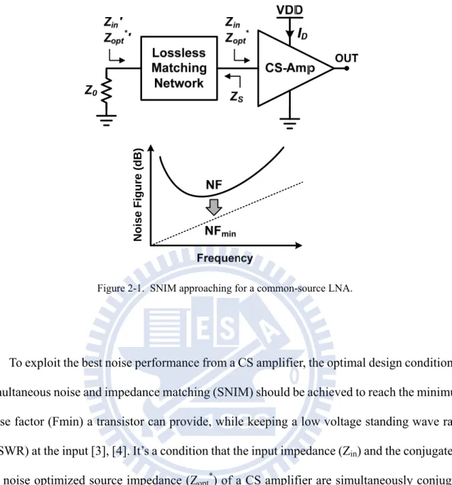
To exploit the best noise performance from a CS amplifier, the optimal design condition of simultaneous noise and impedance matching (SNIM) should be achieved to reach the minimum noise factor (Fmin) a transistor can provide, while keeping a low voltage standing wave ratio (VSWR) at the input [3], [4]. It’s a condition that the input impedance (Zin) and the conjugate of the noise optimized source impedance (Zopt*) of a CS amplifier are simultaneously conjugate matched to an impedance ZS, and then matched to the source impedance Z0 by a lossless matching network, as shown in Figure 2-1. As such, the amplifier noise figure approaches to the minimum level. Typically the SNIM condition can occur with a feedback technique. A widely used one for narrowband LNA design is a CS amplifier with inductive source degeneration, which has been well analyzed [1], [5], [6]. In those papers the induced gate noise of a MOS transistor was emphasized as the root cause of mismatch between Zin and Zopt*. Because the frequency dependency of the derived Zopt is different from that of Zin, broadband SNIM (BSNIM) is not feasible using that technique. This is observed in the broadband amplifier
Noise Figure (dB)
realized by employing a multi-order LC matching network [7], of which noise performance is still band-limited. In 2006, two UWB LNAs utilizing distinct transformer feedback structures were reported [8], [9], both showing broadband noise performance. In [8] we demonstrated the first BSNIM LNA by employing dual reactive feedback topology. We infer the work in [9] might also achieve BSNIM as two reactive feedback paths are employed in the first stage, although this was not discussed by the authors.
In this chapter the theory for BSNIM realization is discussed in details. Before the derivation it’s meaningful to understand the noise model of a MOS transistor in deep submicron CMOS technology, and keep in mind under what condition the derived equations for BSNIM are valid and accurate. This will be discussed in the next section. Then we will analyze the practical mechanisms jeopardizing the ideal SNIM condition inside a CMOS transistor, including the effects of the gate resistance, gate-to-drain capacitance, and induced gate noise. Based on the derived four noise parameters, the strategies to achieve SNIM are proposed for both narrowband and broadband applications as design guidelines. In the following section a dual reactive feedback amplifier with LC ladder matching network is proposed to achieve BSNIM. The feedback circuit converges to a transformer for area compactness. This circuit topology is applied to realize a 3-11GHz ultra-wideband LNA and a 2-6GHz reconfigurable LNA [10], which will be detailed in the following chapters.
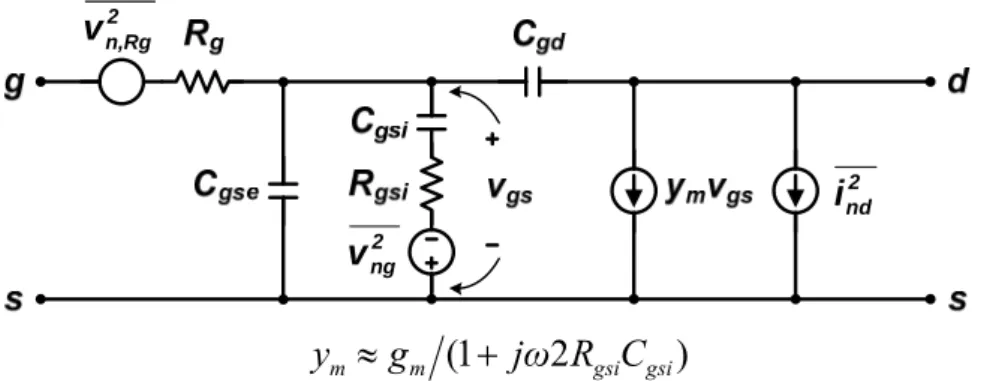
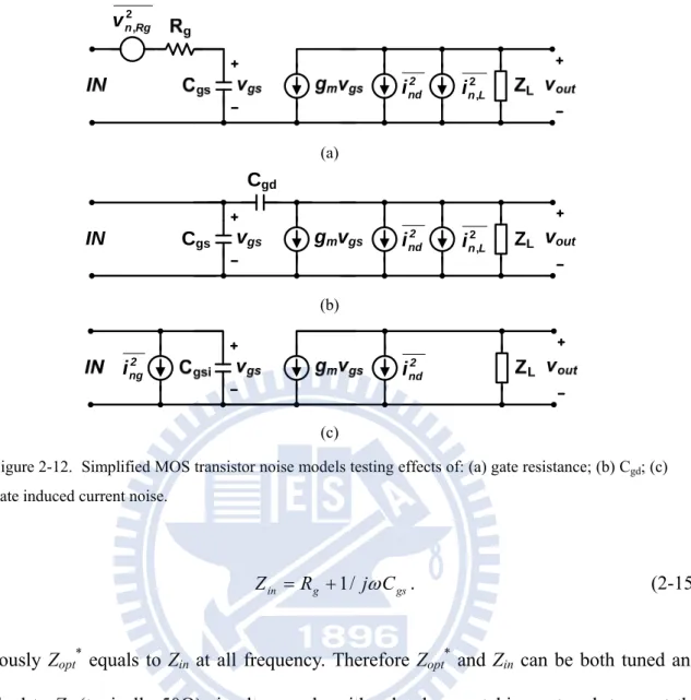
2 nd i 2 ng i 2 n,Rg v
2.2 Noise Model of a MOS Transistor in Deep Submicron
MOS Technology
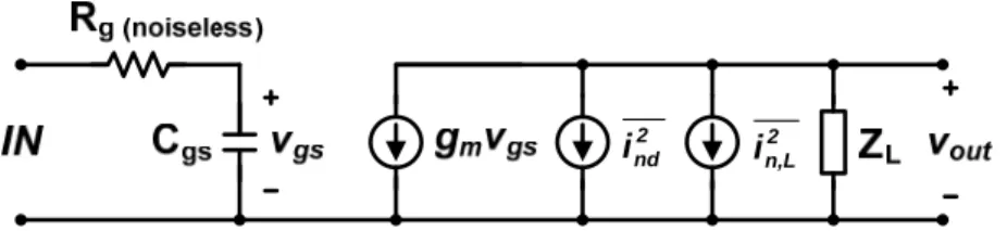
The noise model of a long channel MOS transistor, as shown in Figure 2-2, has been widely used in the common-source based LNA design [1], [2]. Three major noise sources are indicated in this model: the channel thermal noise 2
nd
i , the induced gate noise 2
ng
i , and the gate
resistance (Rg) associated noise v , of which values are formulated as Rg2 ind =4kTγgdo⋅Δf 2 , (2-1) f g C kT f g kT i do gsi g ng = ⋅Δ = ⋅Δ 5 4 4 2 2 2 δ δω , (2-2) and vRg2 = 4kTRg ⋅Δf . (2-3)
Here gdo is the drain-to-source channel conductance in strong inversion with zero VDS. The Cgsi
is the intrinsic gate-to-source capacitance via channel. The γ and δ are derived as 2/3 and 4/3
respectively for long channel MOS transistor. Because 2
nd
i and 2
ng
i are introduced by the same
channel resistance, they are partially correlated to each other with the correlation factor defined as , . 2 2 * i nd ng nd ng jc i i i i corr = ⋅ = (2-4)
the capacitive coupling via Cgsi. The directions of ind2 and
2
ng
i in Figure 2-2 decide the sign of the
correlation factor.
For deep submicron MOS transistors, short channel effects such as channel length modulation (CLM), carrier velocity saturation, and drain induced barrier lowering (DIBL) should be considered in noise model. These effects are manifest in a significant rise of the γ in (2-1). In the beginning such rise of γ was inferred attributed to the hot carrier effect [11]. In 2002 Chen and Deen showed that the increase of γ can be modeled in charge sheet model with CLM and is irrelevant to the hot carrier [12]. To include short channel effects in a simplified equation for circuit designers, Cui et al. tried to replace the γ·gdo with γgm·gm in (2-1) [13].
However, with an increased Vgs, the channel thermal noise was found keeping increasing while
the gm has been saturated. This makes the γgm dependent to Vgs as well as transistor spice model
hence not able to be predicted by hand calculation. In this section, we qualitatively interpret short channel effects in noise model to gain some insight.
Figure 2-3 is a cross-sectional view of a deep submicron MOS transistor in saturation mode with channel in moderate to strong inversion. The channel can be divided into two regions: a gradual charged region of length Lelec = Leff – ΔL (the region I in Figure 2-3) and the
velocity saturated region of length ΔL (the region II), which emerges when VDS is larger than
VDSsat. It is found, while the region I follows Ohm’s law with associated thermal noise, the
region II doesn’t introduce noise [12]. The noise level of a MOS transistor is determined by the charge in region I only.
If the saturation is simply caused by pinch-off, i.e., VDG > -Vth, such that no charge resides
δ, and ci of 2/31, 4/3, and 5 32, respectively, can be obtained for (2-1), (2-2) and (2-4). In
presence of carrier velocity saturation, the drain current saturates before the pinch-off occurs, i.e., VDG < Vth. There are charges resident in region II in such case but those charges are
confined to the speed limit hence contribute no noise, either. The charge distribution in region I is relatively plane, like the curve b in Figure 2-3, such that the γ is close to 1 if ΔL ~ 0.
The more significant increase in γ is caused by DIBL: the electric field by the drain voltage actually increase the charge in region I, like the curve c in Figure 2-3. The effect of drain voltage on the charge, as well as the corresponding γ, also saturates when VDS > VDSAT because
1 The γ of 2/3, derived by integrating the inverted charge, is the same 2/3 in the expression of Cgsi = (2/3)·WLCox in saturation mode.
the region II absorbs the excessive voltage drop. Therefore the γ value by DIBL depends on the CMOS process and channel length. For circuit designers the γ value can be obtained via simulation at VDS=VDSAT, if the spice model provides an accurate noise model.
The last effect to be considered is CLM. When ΔL > 0 by CLM, the channel noise is also increased as DSAT V nd elec eff nd i L L i2 = ⋅ 2 . (2-5)
With the relationship [14]
DSAT D elec eff I I L L = , (2-6)
the γ in (2-1) can be rewritten to be DSAT V DSAT D I I γ γ = ⋅ , (2-7)
where IDSAT is the ID when VDS = VDSsat. The relationship in (2-6) also holds in carrier velocity
saturation situation.
The induced gate noise, in contrast to the channel thermal noise, is decreased by short channel effects as the effective channel resistance in region I is decreased by the increased charge. The decrease of δ in (2-2) can be inferred in proportional to the increase of γ. Hence the induced gate noise has been argued ignorable in deep submicron process [15], [16]. However in this thesis we still preserve the effect of induced gate noise for the possible case of very high frequency applications.
In SPICE model the induced gate noise is the associated noise of the non-quasi-static (NQS) effect of a MOS transistor in high frequency operation [14]. Figure 2-4 shows the simplified noise model in non-quasi-static (NQS) form. The Rgsi is equal to the inverse of gg in
(2-2) with associated voltage noise
f g kT f R kT v do gsi ng = ⋅Δ = ⋅Δ 5 1 4 4 2 δ δ . (2-8)
In addition to the associated noise sources, the metal overlap parasitic capacitances such as the gate-to-drain (Cgd) and the extrinsic gate-to-source (Cgse) capacitances are also included in this model as they are very significant in advanced CMOS technologies. The model in Figure 2-4 is useful for noise analysis in circuit simulator. However for hand calculation the approximated version with the term of induced gate noise in Figure 2-5 is more convenient. The difference between Figure 2-4 and Figure 2-5 is ignorable at frequency much smaller than 5·fT.
) 2 1 ( gsi gsi m m g jω R C y ≈ + 2 ng v 2 nd i 2 n,Rg v
Figure 2-4. Simplified non-quasi-static transistor model of a MOS transistor;
2 n,Rg v 2 nd i 2 ng i
The model in Figure 2-5 will be used for noise derivation in the succeeding sections.
One should keep in mind that the equations (2-1) and (2-2) are only valid for a MOS transistor biased in strong inversion. When it is biased in moderate inversion or weak inversion, the gdo is no longer adequate to evaluate the channel noise. This is because the drain voltage
affects channel charge (DIBL) so significantly, sometimes even overwhelms the effect by gate voltage. In consequence, the γ associated with gdo becomes a function of drain voltage. In such
case, the γgm·gm instead of the conventional γ·gdo could be a better representation of channel
noise [13].
2.3 Noise Analysis Technique for Noise Parameters
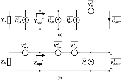
Noise parameter analysis is the most critical step to explore the solution for BSNIM. Noise parameters are those parameters indicating the effect of source impedance to noise factor. The widely used Y-parameter representation of noise parameters is derived by analyzing the output
2 c n, i 2 n v 2 s n, i in,2u in,2out (a) 2 n i 2 u n, v 2 s n, v vn,2c 2 out n, v (b)
Figure 2-6. The two different representations of noise parameters: (a) Y-parameter representation; (b) Z-parameter representation.
noise current, as shown in Figure 2-6(a). The noise factor (F) equation in noise parameters is [3] 2 min S opt S n Y Y G R F F = + ⋅ − . (2-9)
Here the Rn is equal to vn2 4kT . On the other hand noise factor can also be represented in
Z-parameter by analyzing the output voltage noise, as shown in Figure 2-6(b), such that
2 min S opt S n Z Z R G F F = + ⋅ − , (2-10)
in which the Gn is equal to in2 4kT . Shooting for BSNIM solution, the Yopt* or Zopt* is the term
we are mostly interested with.
2 L n, i 2 nd i 2 R n, g v
(
2)
2 , 2 2 ,g nd nL m n i i g v = + 2 g n, v 2 ng i (a) 2 n,Rg v vn,2g 2 ng i (b)Figure 2-7. The proposed derivation technique for noise parameters: (a) The general case for the CS amplifier with lossless feedback network; (b) Equivalent circuit for noise derivation.
To accurately derive the noise parameters of an amplifier, the input-referred noise sources should be obtained first. The general measure is to calculate the corresponding output noise voltages for the short-circuited and open-circuited input individually first, then divide them by signal gain to obtain the input-referred voltage and current noise sources, respectively [17]. This generalized method, however, is not favorable to hand derivation because it makes the equations very complicated hence one is easy to loss the physical insight of components for the
Zopt* (or Yopt*).
The proposed noise analysis technique for a CS amplifier with reactive feedback includes the noise model simplification and the equivalent noise source conversion. The former is illustrated in Figure 2-7. In Figure 2-7(a) is the general case of a CS amplifier with reactive feedback networks, in which the 2
, g
n
v is the equivalent gate noise source representing the noise contribution by the ind2 and
2 ,L n i , which is.
(
2)
2 , 2 2 ,g nd nL m n i i g v = + . (2-11) If |YFP| and |ZFS| are much smaller than gm and 1/gm, respectively, the noise model in Figure2-7(a) can be approximated to the equivalent circuit shown in Figure 2-7(b). The derivation of input referred noise sources therefore can be simplified and starts from the input of the voltage controlled current source, i.e. the vgs. It is obvious that the real parts of YFP and ZFS contribute
noise to the input network and deteriorate noise performance directly hence a pure reactive feedback is preferred for LNA design. When this model is projected to the transistor noise model in Figure 2-5, the Cgd plays the role of YFP, and the ZFS is equal to 0. Noted that the
equivalent circuit in Figure 2-7(b) is only for noise analysis – it cannot be used for input impedance analysis.
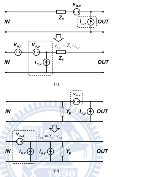
source conversion, a derivative concept of equivalent noise fourpoles [18], can be applied. As shown in Figure 2-8(a), the shunt current noise source in,y after a series passive device Zp has input-referred noise sources including the original in,y and a series voltage noise source vn,y fully
correlated to in,y, whereas the series voltage noise source vn,x remains unchanged at input. Then
the total input-referred voltage noise source vn,i can be obtained by combining vn,x and vn,y. Note
that the direction of the noise sources in Figure 2-8 carries the correlation information between noise sources.
The combination of v and v should be proceeded by employing vector operation, as x n, v y n, i x n, v y n, i y n, v vn,y =Zs⋅in,y (a) n,x p n,x Y v i = ⋅ x n, v y n, i x n, v y n, i x n, i (b)
Figure 2-8. Two fundamental cases of equivalent noise sources conversion over passive devices: (a) series device; (b) shunt device.
shown in Figure 2-9, whether the vn,x and in,y are correlated to each other or not. Assume any
vector along the direction of unit vector aˆy is fully correlated to in,y, then the vn,x can be seen as
combination of two orthogonal vectors along directions aˆy and aˆz, in which vectors along aˆz
have no correlation to in,y. The correlation factor cxy between vn,x and in,y is equal to cosθ0. After vector addition with vn,y
G , as shown in Figure 2-9, the total voltage noise source v
n,i can be
obtained with the correlation to in,y of factor ciy equal to cosθ1.
The equivalent noise sources conversion over a shunt passive device can be derived in the x n, xy yc v aˆ G x n, 2 xy z 1-c v aˆ G y n, s y y n, a Z i vG = ˆ G x n,
v
G
v
n,iG
y aˆ z aˆFigure 2-9. Vector operation to combine two partially correlated noise sources.
⎥ ⎦ ⎤ ⎢ ⎣ ⎡ D C B A ⎥ ⎦ ⎤ ⎢ ⎣ ⎡ D C B A n,2 v n,2 i n,1 v n,1 i
same manner, as shown in Figure 2-8(b). Noise contribution from Zs and Yp in Figure 2-8 can be included in the vn,x and in,y, respectively. The general form of this conversion is shown in
Figure 2-10, in which
⎥
⎦
⎤
⎢
⎣
⎡
⎥
⎦
⎤
⎢
⎣
⎡
=
⎥
⎦
⎤
⎢
⎣
⎡
2 , 2 , 1 , 1 , n n n ni
v
D
C
B
A
i
v
G
G
G
G
(2-12)with correlation factor
1 , 1 , 1 , 1 , 2 1 , 2 1 , * 1 , 1 , . n n n n n n n n i v i v i v i v corr G G G G ⋅ = ⋅ ⋅ = . (2-13)
In (2-13) the dot in the numerator is the symbol of vector inner product. To reduce the unnecessary calculation complexity, it is better to keep those independent noise sources apart during derivation of the total input referred noise sources, i.e., retain noise sources in either fully correlated or uncorrelated types. Only combine those sources when necessary in the derivation. After the input referred noise sources obtained, Zopt* (or Yopt*) and other noise
parameters can be accurately derived with the two-port noise theory introduced in [3].
2.4 SNIM for a CS Amplifier – The Problem and the
Solution
In the microwave theory, a CS amplifier is designed either gain-optimized by impedance matching or noise-optimized by noise matching [3]. In LNA design the latter is more important since a low noise figure is demanded. The impedance matching of an LNA is simply for a minimized input reflection for a low VSWR such that the random length of a transmission line
noise optimized – it is to optimize the noise performance first, then design for a small input reflection with a feedback technique, by which the gain is slightly suppressed.
The exploration toward the BSNIM design necessitates derivation of input-referred noise sources for the noise parameters. All the noise parameters in this section are derived based on the analysis technique described in the previous section. Some reasonable simplification can be applied with the numerical approximation in the noise parameter equations. Then by analyzing
Zin and Zopt* the strategies for BSNIM can be mapped out.
2.4.1 Mismatch between Z
inand Z
opt*of a CS MOS Amplifier
The mismatch between Zin and Zopt* of a CS amplifier is well known but was not well
analyzed. To identify the factors causing such mismatch we start our discussion from a special case that always meets the SNIM condition, i.e., Zin = Zopt*. Consider the ideal hybrid-π model
of a MOS transistor, shown in Figure 2-11, which includes 2
nd
i , 2 ,L
n
i , and a noiseless gate resistor Rg. By applying the noise analysis technique in the previous section, Zopt* of this ideal
transistor can be derived to be
gs g opt R j C Z* = +1/ ω , (2-14) and Zin is 2 L n, i 2 nd i
Zin =Rg +1/ jωCgs. (2-15)
Obviously Zopt* equals to Zin at all frequency. Therefore Zopt* and Zin can be both tuned and
matched to Z0 (typically 50Ω) simultaneously with a lossless matching network to meet the
SNIM condition.
In the practical case, as shown in Figure 2-5, Zopt* and Zin are found apart from each other
by three major factors, referred to as Zin-to-Zopt* discrepancy factors: 1) independent noise
sources at the gate, 2) gate-to-drain capacitance, and 3) induced gate noise. Effects of these three factors can be observed individually by the three test cases as shown in Figure 2-12.
The first one is the independent noise sources at the gate port. The typical one is the gate resistance noise 2
,Rg n
v . Using the noise model as shown in Figure 2-12(a), the analysis shows that
Z * is significantly changed and derived as
2 ,L n i 2 ,Rg n v 2 nd i (a) Cgs vgs gmvgs in2,L Cgd ZL vout 2 nd i IN (b) 2 nd i 2 ng i (c)
Figure 2-12. Simplified MOS transistor noise models testing effects of: (a) gate resistance; (b) Cgd; (c) gate induced current noise.
gs gs m L n d n g g opt C j C g i i f kTR R Z ω ω 1 4 2 2 , 2 , 2 * + ⎟ ⎟ ⎠ ⎞ ⎜ ⎜ ⎝ ⎛ ⋅ + Δ + = . (2-16)
In comparison to (2-14), the noise source 2 ,Rg
n
v increases the real part of Zopt* with a
frequency-dependent term and thus makes Zopt* larger than Zin. This factor is found to be the
primary factor to Zin-to-Zopt* discrepancy in most CMOS LNA design. The noise from a
non-ideal input matching network also contributes the same effect.
The second factor is the parasitic feedback via gate-to-drain capacitance Cgd. The feedback
loop gain changes Yin (the inverse of Zin) without affecting Yopt* (the inverse of Zopt*). Consider
the simplified transistor noise model with Rg= 0 as in Figure 2-12(b). It can be found that
) ( * gd gs opt j C C Y = ω + , (2-17) and L gd L m gd gs in Z C j Z g C j C j Y ω ω ω + + + = 1 1 . (2-18)
With Miller effect, the loading of impedance ZL modifies Cgd in Yin via the Cgd feedback.
The third factor is the induced gate noise. Consider the noise model with Rg= 0 as in Figure
2-12(c). Cgse, Cgd, and in2,L are ignored. The derived Yopt
* is approximately as
(
)
⎟⎟ ⎠ ⎞ ⎜⎜ ⎝ ⎛ ⋅ − + − ⋅ ≈ γ δ α ω γ δ α ω 5 1 1 5 2 * i gsi i gsi opt C c j C c Y , (2-19)in which α=gm /gdo. It is beneficial to define the output noise contribution ratio of ing2 to
2
nd i as
(
)
γ δ α ω κ 5 2 2 2 = ⋅ = nd gsi m ng i C g i . (2-20)Yopt* in (2-19) then can be simplified as
(
κ)
ω κ ω gsi i gsi i opt C c j C c Y* ≈ 1− 2 + 1− . (2-21)By comparing this Yopt* with the corresponding Yin, equal to jωCgs, the induced gate noise is
found reducing the effective capacitance of Yopt* and introduces a frequency dependent real part
on Yopt*.
Now consider the equivalent circuit in Figure 2-5 with Rg and ZL both equal to zero. Define
ρ as the noise contribution ratio,
(
2)
, 2 2 L n nd nd i i i + = ρ , (2-22)a value smaller than 1. Yopt* can be derived as
( )
i(
gs gd i gsi)
gsi
opt C c j C C c C
Y* ≈ω ρκ 1− ρ 2 + ω + −ρ2 κ . (2-23)
By comparing (2-23) with (2-21) it can be observed that Cgse, Cgd, and in2,L all mitigate the
effect of 2
ng
i on Yin-to-Yopt* discrepancy.
With all the three factors and 2 ,L
n
i considered, it can be derived that
N N m L n nd g g opt j C c C c g i i f kTR R Z ω ω2 2 1 2 1 2 2 , 2 2 * 4 1 1 + ⎟ ⎟ ⎠ ⎞ ⎜ ⎜ ⎝ ⎛ − + + Δ + = , (2-24) in which
(
)
2 2(
)
2 2 2 2 i gsi gs gd gsi gd gs N C C c C C C C C = + − ρ κ + +ρ κ (2-25) and(
)
2 2 2 2 2 2 1 1 1 N gsi i C C c c = − −ρ ρ κ . (2-26)With the typical device values in 0.18um CMOS technology, CN and c1 are about 0.94·(Cgd+Cgd) and 0.98, respectively. More than 99.5% of Re{Zopt*} comes from its second
term in (2-24). Hence Zopt* can be approximated as
) ( 1 4 ) ( 2 , 2 * gd gs L n nd g gd gs m opt C C j i i f kTR C C g Z + + + Δ + ≈ ω ω . (2-27) If 2 ,L n
i is assumed frequency-independent, Zopt* has a frequency-independent quality factor.
Hence in Smith Chart the Sopt* curve follows the constant-Q contour, completely different to the
behavior of a normal RC network.
The other noise parameters are obtained as well. In the Z-parameter representation of the noise factor of 2 min S opt S n Z Z R G F F = + ⋅ − , (2-28)
the Gn and Fmin are
2 2 2 2 , 2 2 2 2 2 2 , 2 4 4 m N L n m N m N L n nd n g C f kT i g C g C f kT i i G ω ω α γ ω ⋅ Δ + = ⋅ Δ + = (2-29)
and
(
)
} Re{ 2 1 } Re{ 2 1 min opt n g opt n Z G R Z G F + ≈ + + = . (2-30)For quick evaluation, Fmin can be simplified by ignoring in2,L as
(
)
g m m gd gs R g g C C F α γ ω + + ≈1 2 min . (2-31)From (2-31) we can see Rg not only introduces Zin-to-Zopt* discrepancy but also directly
deteriorates Fmin. Rg is therefore identified as the dominant noise contributor to an LNA. On the
other hand, Zin is derived as
L gd L m gd gs g in Z C j Z g C j C j R Z ω ω ω + + + + = 1 1 1 . (2-32)
The accuracy of (2-24)–(2-26) was verified with several test cases by MATLAB and Agilent ADS. The calculated Sopt* (S-parameter of Zopt*) well matches the simulated Sopt*.
Representative results are plotted in Figure 2-13. In this test case the component parameters in the model of Figure 2-5 were extracted from a 0.18μm NMOS transistor operated in strong inversion and saturation mode, then applied to (2-24) for calculation and the model in Figure 2-5 for simulation. The simulation result with the foundry noise model is also included as reference. Different test conditions are applied to analyze the factor effects. As can be seen, the calculation result fits the simulation results very well. The Sopt* curve behaves as a constant-Q
curve, showing a strongly frequency-dependent Re{Zopt*}, not matched to the S11 curve at all.
The Rg dominates the real part discrepancy, whereas the induced gate noise i has just ng2 marginal effect on Sopt*. Different values of ZL are used to observe the effect of Cgd feedback on
Zin. It can be observed that Im{Zin} is significantly affected by a resistive ZL because of the Cgd
feedback, while the Re{Zin} is also slightly affected, as can be predicted from (2-32). In
addition, if a reactive ZL is applied, a capacitive ZL provides an additional noiseless resistance
whereas an inductive ZL conducts a positive feedback causing an unstable resonance. The
former can be utilized for BSNIM as described in next section.
By comparing Zopt* and Zin among (2-24), (2-27) and (2-32), respectively, their difference
can be briefly summarized as:
1) To the real part, the noise contributed by Rg makes Re{Zopt*} much larger than Re{Zin} by a
frequency-dependent amount.
2) To the imaginary part, with a resistive ZL the Cgd feedback makes Im{Zin} smaller than
Im{Zopt*}. When represented by series capacitance, the equivalent series capacitance in Zin
Sopt* (Fundary Noise Model) Sopt* (Equation 2-24.)
S11 (Sim., ZL=50mΩ)
S11 (Sim., ZL=50Ω)
Sopt* (Sim., Excluded)ing2 Sopt* (Sim., Model in Fig. 2-5)
Figure 2-13. Equation verification of Zopt* and the analysis of discrepancy facter effects on Smith Chart. Frequency swept from 1 to 20GHz with 1GHz step.
is larger than that in Zopt .
The other important factor concerned is the gain of the first amplifying stage. If the gain is not high enough to suppress noise contribution of succeeding stages, a larger 2
,L
n
i will be introduced and in consequence Fmin is deteriorated, too.
2.4.2 Strategies to Achieve BSNIM
With the mechanism of Zin-to-Zopt* discrepancy identified, strategies to achieve BSNIM
for minimized noise figure can be mapped out. For the real part, because Re{Zin} is smaller than
Re{Zopt*}, the difference can be compensated by introducing a noiseless resistance with a
reactive feedback technique. As to the imaginary part, it is critical to minimize the impact on the series capacitance expansion of Zin induced by Cgd and the real part of ZL. From (2-27) and
(2-32), it is necessary to meet the following condition as
gd L m L C Z g Z ω 1 } Re{ and 1 } Re{ << << . (2-33)
The proposed SNIM strategy matches Zopt* to the source impedance Z0 first, then uses reactive feedback to match Zin to Z0 without affecting Zopt* and the minimum noise figure. For a
narrowband LNA at frequency f0, the design criteria for SNIM are summarized as follows:
1) Apply the least channel length for the best transistor performance. From (2-31) the Fmin increases roughly with
(
Cgs +Cgd)
Rg gm , which can be minimized with the least channel length.2) The real part of ZL should be as small as possible, not to expand the difference between
3) Given specified drain current, co-design the transistor size and matching network to make Zopt* matched to the source impedance Z0 at f0.
4) Increase Re{Zin} to match Z0 without adding noise and changing Re{Zopt*}. This can be
achieved by employing reactive feedback technique. The well known is the inductive
source degeneration technique.
For a prescribed DC drain current (power constraint), Zopt* is adjusted by varying the
transistor size. If the transistor size is increased, gm increases, Rg decreases, and fT decreases. From (2-27) and (2-31), Re{Zopt*} decreases but Fmin increases. Nonetheless, such Fmin increase
is insignificant as compared to the noise factor improvement by noise matching2. For applications of f0 << fT, such adjustment leads to an extremely low transistor current density (weak inversion), which may severely suffer from process variation and induce unacceptable non-linearity. In such case an external capacitor in parallel to the transistor Cgs to lower fT is favorable. Similarly it increases Fmin slightly but helps keep noise matching with a transistor in moderate inversion.
For broadband applications, both Zopt* and Zin need to be close to Z0 over the entire bandwidth. This requires a high-order input matching network. Equation (2-27) and (2-32) show the frequency dependencies of Re{Zopt*} and Re{Zin} are different. Hence the reactive
feedback, as described in the item 4) above, needs to increase Re{Zin} by a frequency dependent
amount. This can be realized by employing multiple reactive feedbacks to make Re{Zin} close
to Re{Zopt*} in different frequency regions. Consequently, the design criteria for BSNIM are
proposed as follows:
2 If large amount of DC power is employed such that the Gn in (2-29) is very small, the noise matching is less appreciable. However, this is
1) Same as the item 1) in narrowband case. 2) Minimize ZL or employ a capacitive ZL.
3) With the drain current specified, the transistor size is chosen to make Re{Zopt*} of the
transistor close to the source impedance Z0 at the center frequency fc of the pass band. Apply
a high-order input matching network (typically a ladder LC network structure) to make Zopt*
close to Z0 in the entire band.
4) Increase Re{Zin} to match Z0 by employing multiple reactive feedbacks.
While multiple reactive feedbacks are necessary for BSNIM, they actually create a high-order impedance function of Zin as a consequence. However the order of Zopt* is not
changed because Zopt* is not affected by the noiseless reactive feedbacks. As such Zin and Zopt*
behave differently on the frequency response. Nevertheless, such difference can be taken care of by the high order input matching network if Zin and Zopt* are both designed close to Z0.
The procedure described above creates a BSNIM LNA which ensures power-efficient noise performance. In the next section an exemplary dual reactive feedbacks technique will be proposed as a BSNIM solution, which has been proven effective for broadband LNA design from 3- to 11-GHz (fractional bandwidth larger than 130%). In comparison to the area-saving but power-hungry resistive/ source-follower feedback amplifier [19]–[22], a SNIM/BSNIM LNA saves lots of power.
2.5 The Proposed BSNIM Amplifier
As discussed above, a BSNIM LNA necessitates a high-order matching network and multiple reactive feedbacks. The proposed BSNIM solution is a LC-ladder matching network
[23] along with a dual reactive feedback topology, composed of a capacitive shunt feedback and an inductive series feedback, as shown in Figure 2-14. The LC-ladder matching network and the dual reactive feedback are co-designed following the BSNIM design criteria in the previous section. Of the dual reactive feedback each feedback attains SNIM in different frequency region for BSNIM. They are seamlessly combined by employing an inductor Ld at the transistor drain port to obtain different loading conditions for each feedback structure. To quantitatively illustrate the design concept, the 3.1 to 10.6GHz UWB LNA designed in 0.18μm CMOS is applied as an example.
2.5.1 The Proposed Dual Reactive Feedback Topology
The proposed dual reactive feedback structure and the LC ladder input matching network results in Zopt* represented by the equivalent circuit as shown in Figure 2-15. Zopt* is not affected
by the lossless reactive feedbacks3. The Zopt*-to-Z0 matching bandwidth is extended by the second-order band-pass LC-ladder structure. The choice of component values follows the guideline as
2 1
1 C (Lg Ls) (Cgs Cgd) 1 (2 fc)
L ⋅ = + ⋅ + = π , (2-34)
in which fc is located at 5.76GHz, the geometric mean of 3.1GHz and 10.6 GHz, in this design.
The bandwidth expansion is determined by the L/C ratios, of which the preliminary values can be obtained by the traditional filter design technique such as Chebyshev filter design. Slight
3 Zopt* is slightly affected by lossless feedbacks because of the degraded gain if the noise from loading stages, i.e. 2
,L
n
i , is included. Nonetheless, such effect is ignorable if this stage provides a sufficient gain.
trimming on LC values can compensate for the frequency dependency of Ropt without problem.
For the optimal broadband matching result, Ropt is in general designed slightly less than Z0 to make the Sopt* curve circling the Smith Chart center over the entire pass-band. The design of L1 and C1 also takes into account the gain response as described later.
While the broadband noise matching is achieved, the input impedance is also matched to
Z0 by the proposed dual reactive feedback circuit, as shown in the dashed-line box of Figure 2-14. A similar circuit structure was proven having the capability of broadband input impedance matching [24]. But different from [24], the proposed approach here is to utilize each reactive feedback in different frequency regions. Such configuration can well minimize the difference between Re{Zin} and Re{Zopt*} over a wide frequency range and therefore enables
BSNIM. In the frequency region much lower than the Ld-CL series resonance frequency, the
Figure 2-14. Proposed BSNIM solution. It consists of a LC ladder matching network and a dual reactive feedback structure, a combination of capacitive shunt feedback and inductive series feedback. The drain inductor Ld is employed for feedback selection and provides band extension on vout.
Ld-CL tank behaves like a capacitor CL' to the transistor. Hence Zin can be represented by the
equivalent circuit shown in Figure 2-16(a), in which
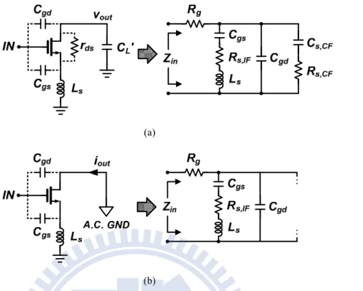
gs s m IF s C L g R, = ⋅ , (2-35) gd m gd L gd m gd L CF s g C C C C g C C R, = '+ ≈ + , (2-36) and gd ds m CF s g r C C , = ⋅ . (2-37) Two noiseless resistances can be found: Rs,IF from the series inductive feedback of Ls, and
Rs,CF from the shunt capacitive feedback of Cgd with CL'. Because Cs,CF in (2-37) is much larger
(a)
(b)
Figure 2-16. Input impedance changed among the two feedbacks with frequency: (a) capacitive shunt feedback in lower frequency region; (b) inductive series feedback in higher frequency region.
than Cgs, the branch of Cs,CF dominates the input impedance in this frequency region such that
Rs,CF is the noiseless resistance contributing to Re{Zin} to match with Ropt.
In the higher frequency region close to the Ld-CL resonance, the output appears as a short
circuit to the drain. Zin can be represented by the equivalent circuit as shown in Figure 2-16(b).
The Cs,CF branch becomes open because the Cgd feedback loop gain is approximately zero. The series inductive feedback is significant under such a condition such that Rs,IF is the dominant
noiseless resistance in this frequency region.
As shown in (2-27), Ropt of the transistor is inversely proportional to frequency. The
variation ratio is larger than 3 over the entire frequency range of interest. To make Re{Zin}
match with Ropt, Rs,IF is designed about a half of Rs,CF, yielding to the required Re{Zin} variation.
In practice, the Cs,CF branch in Figure 2-16(a) has a low Q property such that the capacitive
feedback is active over a good portion of the frequency range.
The placement of L1, C1, and Lg takes care of Im{Zin}, making Zin also close to Z0 over the entire frequency range. Actually Lg results in two resonance frequencies with the transistor
circuit. At low frequencies of capacitive feedback, Lg and Cs,CF constitute a resonance tank with
the resonance frequency of
gd ds m g CF s g CF L C L g r C f0, =1 2π , =1 2π ⋅ ⋅ . (2-38)
For the inductive feedback, the resonance frequency is located at a higher frequency at ) || ( ) ( 2 1 1 , 0 L L C C f IF = π g + s ⋅ gs . (2-39)
Therefore the frequency dependence of Zin turns out to be an order higher than that of Zopt. In
this design f0,CF and f0,IF are located at 5GHz and 9GHz, respectively. As to the choice of Ld, it is
2 , 0 ) 2 ( 1 IF L d C f L ⋅ ≈ π . (2-40)
2.5.2 Gain Response
As mentioned in the previous section, a sufficiently high gain over the entire band is necessary to suppress the noise contribution of 2
,L n
i . The proposed BSNIM amplifier is expected to fulfill such a gain requirement. Its design concept is shown in Figure 2-17. The gain response is mainly shaped by the drain network in Figure 2-14 as the input network is a broadband structure. Based on the low-pass response by CL (the gray curve in Figure 2-17), Ld conducts a
series gain peaking at the frequency
) || ( 2 1 , 0Peak Ld Cgd CL f = π ⋅ , (2-41)
which is higher than f0,IF in (2-39). The voltage gain at this frequency can be derived with the
circuit approximation as shown in Figure 2-18, in which
gd m gd gs d C g C C R '≈ + . (2-42)
Figure 2-17. Gain response of the proposed BSNIM amplifier. The low-frequency gain is suppressed by L1 and the high-frequency gain is enhanced by Ld.