國
立
交
通
大
學
電機學院 電機與控制學程
碩
士
論
文
應用在薄膜電晶體液晶顯示器驅動積體電路之
雙邊雙輸出切換電容式電壓轉換器
Dual Side Dual Output Switching Capacitor Voltage Converter
for TFT-LCD Driver IC
研 究 生:林洋慶
指導教授:陳科宏 博士
應用在薄膜電晶體液晶顯示器驅動積體電路之
雙邊雙輸出切換電容式電壓轉換器
Dual Side Dual Output Switching Capacitor Voltage Converter
for TFT-LCD Driver IC
研 究 生:林洋慶 Student:Yang-Ching Lin
指導教授:陳科宏 Advisor:Ke-Horng Chen
國 立 交 通 大 學
電機學院 電機與控制學程
碩 士 論 文
A Thesis
Submitted to College of Electrical and Computer Engineering
National Chiao Tung University
in partial Fulfillment of the Requirements
for the Degree of
Master of Science
in
Electrical and Control Engineering
December 2010
Hsinchu, Taiwan, Republic of China
應用在薄膜電晶體液晶顯示器驅動積體電路之雙邊雙輸出切換電
容式電壓轉換器
研究生:林洋慶
指導教授:陳科宏 博士
國立交通大學 電機學院 電機與控制學程碩士班
摘 要
近年來,薄膜電晶體液晶顯示面板已經成為移動或手持式電子,諸如行
動電話、MP3 播放器、數位像機、PDA 以及筆記型電腦等,最重要的螢幕顯
示元件。薄膜液晶顯示面板以高亮度、高彩度、反應速度快、低成本以及
長壽命等優點擊敗了許多諸如超扭轉向列型以及有機發光二極體等顯示面
板。因此薄膜液晶顯示驅動積體電路產業非常充滿活力。
切換電容式電壓轉換器又稱為充電幫浦,是最常應用在手持薄膜電晶體
液晶顯示驅動積體電路的電源產生器。電壓轉換器是用來將系統輸入電壓
轉換成高電壓,或甚至是負電壓,以供薄膜電晶體液晶顯示驅動積體電路
的閘級驅動電路、源級驅動電路以及面板共電極參考電壓驅動電路等使用。
傳統的雙邊兩倍壓電壓轉換器利用兩個機動電容器來產生系統的兩倍
電壓,傳統的雙邊電壓反向轉換器也是利用兩個機動電容器來產生系統的
負一倍電壓。本論文提出了一個雙邊雙輸出電壓轉換器,並且成功的應用
在以 SilTerra 0.13um 1.8V/5V/32V CMOS 1P5M 製程實現的 QVGA 解析度的
薄膜電晶體液晶顯示驅動積體電路。這個新提出的電壓轉換器只需使用兩
個機動電容器來同時產生兩倍以及負一倍的系統電壓。同時,此電壓轉換
器比傳統的電壓轉換器節省了超過 27%的積體電路佈局面積、四個積體電路
輸出入阜以及兩個外部電容元件,降低了生產成本。
Dual Side Dual Output Switching Capacitor Voltage Converter for
TFT-LCD Driver IC
Student: Yang-Ching Lin
Advisor: Dr. Ke-Horng Chen
Degree Program of Electrical and Computer Engineering
National Chaio Tung University
Abstract
In recent years, as a display screen, the thin film transistor-liquid crystal display (TFT-LCD) panel becomes the most popular element for mobile or handheld devices such as cell phones, mp3 players, digital cameras, PDAs, laptops, …etc. With the advantages of high brightness, rich color depth, fast response time, low cost and long life time, the TFT-LCD panel had defeated many competitors such as the super twisted nematic (STN) and the organic light emitting diode (OLED) display panel. As a result, the industry of TFT-LCD Driver is full of vigor and vitality.
The switching capacitor voltage converters which are also named the charge pumps are most commonly used in the hand-held TFT-LCD drivers for generating the power supply. The voltage converters are used to transform the system input voltage level into a higher voltage level or even a negative voltage for the use of some function blocks of the TFT-LCD drivers such as the gate drivers, the source drivers and the VCOM drivers.
The conventional dual side voltage doubler uses two flying capacitors to generate two times the system input voltage and the conventional dual side voltage inverter also uses two flying capacitors to generate negative time the system input voltage. In this thesis, a dual side dual output voltage converter is proposed. This new voltage converter is successfully implemented in a QVGA resolution TFT-LCD and is fabricated with SilTerra 0.13um 1.8V/5V/32V CMOS 1P5M process. This new proposed voltage converter uses only two flying capacitors to generate two times and negative time the system input voltage, and in the meantime, the new voltage converter saves over 27% IC layout area, 4 IC pin outs and 2 external capacitors than the conventional converters and reduces the cost.
誌謝
唐代青原惟信禪師曾云:「老僧三十年前來參禪時,見山是山,見水是
水;及至後來親見知識,有個入處,見山不是山,見水不是水;而今得個
休歇處,依然見山只是山,見水只是水。」
在「見山是山」,追求知識的初期,人都只是看到了事物的表象,見到
了什麼就認為是什麼,由於缺乏知識,判斷真假是非對錯的能力不足。到
了「見山不是山」,追求知識的中期,由於得到了一些知識,開始學習如
何判斷真假是非對錯,人就開始對事物充滿了懷疑,不再相信眼前所見到
的事物。到了「見山依然是山」,追求知識的後期,人經歷過了對事物的
懷疑與格物致知後,由於得到了許多知識並加以融會貫通,可以透徹了解
事物的本質。
在職場奮鬥數年的我,正處於「見山不是山」這個十分需要良師的的階
段。非常感謝指導教授 陳科宏博士在我人生的這個階段給予細心的指導
與諄諄的教誨,讓我在茫茫學海中,找到了一盞明燈。俗話說「師父引進
門,修行靠個人」。雖然我距離「見山依然是山」的境界尚遠,但仍感謝
教授這三年的指導,給予了我一個明確的方向,讓我可以朝著目標前進。
感謝奕力科技的長官王建國處長、余錦旗經理與慶造、良榕、清榮、庭
甫、志飛、世璋、文輝、信僥等好同事們,有你們在我求學之路上的打氣
與支持,讓我得以完成學業。
另外,也要感謝在職專班與 Lab912 的學長、同學、學弟們這幾年來對
我的照顧與幫忙,讓我能夠順利畢業。
感謝我親愛的父親林通進與母親王金女,有了你們無怨無悔的付出、提
攜與養育,才有今天的我。也要感謝我的家人,給我的支持與鼓勵。
我要將這份榮耀與我最親愛的老婆翊榛一起分享。感謝妳在我人生路上
與我並肩攜手同行,分擔我的酸甜苦辣,多次使我打消了休學的念頭。因
為有妳,才讓我有動力完成碩士學位!三言兩語難以道盡我對妳的愛與感
激。這些年來真是辛苦妳了,謝謝妳!
最後,我要感謝南無大慈大悲觀世音菩薩,在我躁鬱難安的時刻,讓
我有澄澈寧靜的思緒,使我產生前進的力量,克服一切阻礙!
Contents
Chapter 1 ...1 Introduction of TFT-LCD Driver...1 1.1 TFT-LCD Driver...1 1.2 Block Diagram...4 1.2.1 Gate Driver ...51.2.2 Gamma Voltage Generator ...7
1.2.3 Source Driver...10
1.2.4 Data Driving Method...12
1.2.5 VCOM Driver...18
1.3 Power Stage Selection ...19
1.3.1 Linear Regulator ...20
1.3.2 Switching Capacitor Converter ...22
1.3.3 Inductor Switching Converter ...23
1.3.4 Power Generation Unit ...26
1.4 Power Specification...29
Chapter 2 ...34
Performance Checking of Switching Capacitor Voltage Converter ... 34
2.1 Basic Concepts about Switching Capacitor...34
2.1.1 Charge Transfer of Capacitors ...34
2.1.2 Switching Capacitor Principle ...36
2.2 Voltage Doubler ...37
2.2.1 Operation of Voltage Doubler...38
2.2.2 Voltage Ripple of Voltage Doubler ...38
2.2.3 Power Loss of Voltage Doubler ...40
2.3 Voltage Inverter ...42
2.3.2 Operation of Voltage Inverter ...43
2.3.1 Ripple of Voltage Inverter ...44
2.3.2 Power Loss of Voltage Inverter ...45
Chapter 3 ...49
Switching Capacitor Voltage Converters in TFT-LCD Driver ...49
3.1 Conventional Voltage Converters ...49
3.1.1 Dual Side Voltage Doubler ...56
3.1.2 Dual Side Voltage Inverter...60
3.2.1 Dual Side Dual Output Switching Capacitor Voltage Converter...63
3.2.2 Comparisons of Conventional and Proposed Voltage Converters ...74
Chapter 4 ...76
Measurements of Switching Capacitor Voltage Converters in TFT-LCD Driver...76
4.1 Conventional Voltage Converters ...77
4.1.1 Dual Side Voltage Doubler ...77
4.1.2 Dual Side Voltage Inverter...80
4.2 New Proposed Voltage Converter...83
Chapter5 ...92
Conclusions and Future Work ...92
5.1 Conclusions ...92
5.2 Future Work ...92
Figure Captions
Fig. 1. TFT-LCD Driver. ...2
Fig. 2. Equivalent Circuit of a Panel. ...3
Fig. 3. TFT-LCD Driver Block Diagrams. ...5
Fig. 4. TFT-LCD Gate Driver. ...6
Fig. 5. Vreg1out regulator: Reference Power of Gamma Voltage Generator. ...8
Fig. 6. Gamma Voltage Generator. ...9
Fig. 7. LC Gamma Curve. ...10
Fig. 8. TFT-LCD Source Driver... 11
Fig. 9. Self-biased Folded Cascode Rail-to-rail Op-amplifier...12
Fig. 10. Inversion Types of TFT-LCD Driver...13
Fig. 11. AC VCOM Driving Method...15
Fig. 12. DC VCOM Driving Method. ...16
Fig. 13. TFT-LCD VCOM Driver...19
Fig. 14. Power supply of Cell Phone System. ...20
Fig. 15. Linear Regulator...21
Fig. 16. Switching Capacitor Converter: Voltage Doubler. ...22
Fig. 17. Inductor Switching Converter: Boost...24
Fig. 18. Power Generation Unit of TFT-LCD Driver. ...27
Fig. 19. Simple Operation Principle of CP1, CP4 and CP23 in TFT-LCD Driver...29
Fig. 20. New Proposed Dual Side Dual Output Charge Pump...31
Fig. 21.Waveforms of Charging a Capacitor. ...35
Fig. 22.Waveforms of Switching Capacitor Operation. ...36
Fig. 23. Voltage Ripple of Voltage Doubler...39
Fig. 24. Steady State Waveforms of Voltage Doubler...41
Fig. 25. Switching Capacitor Voltage Converter: Voltage Inverter. ...43
Fig. 26. Voltage Ripple of Voltage Inverter. ...45
Fig. 27. Power Loss of Voltage Inverter. ...46
Fig. 28. Conventional Voltage Converters...50
Fig. 29. Clock Phase Generation Circuit. ...51
Fig. 31. LSH_P6V Level Shifter. ...53
Fig. 32. Simulation Result of LSH_P6V Level Shifter. ...54
Fig. 33. LSH_N3V Level Shifter...55
Fig. 34. Simulation Results of LSH_N3V Level Shifter. ...56
Fig. 35. Power Switches of Dual Side Voltage Doubler...57
Fig. 36. Simulation Result of Dual Side Voltage Doubler...58
Fig. 37. Power Switches of Dual Side Voltage Inverter. ...60
Fig. 38. Simulation Result of Dual Side Voltage Inverter. ...61
Fig. 39. Dual Side Dual Output Voltage Converter. ...64
Fig. 40. Clock Phase Generation Circuit. ...65
Fig. 41. Simulation Result of Clock Phase Generation Circuit. ...66
Fig. 42. Power Switches of Dual Side Dual Output Voltage Converter. ...67
Fig. 43. Simulation Results of Dual Side Dual Output Voltage Converter. ...68
Fig. 44. Simulation Results of Dual Side Dual Output Voltage Converter: DDVDH only...69
Fig. 45. Simulation Results of Dual Side Dual Output Voltage Converter: VCL only. ...72
Fig. 46. Layout of the Conventional Voltage Doubler and Voltage Inverter. ...76
Fig. 47. Waveform Measurements of the Conventional Dual Side Voltage Doubler. ...77
Fig. 48. DDVDH Load Regulation of the Conventional Dual Side Voltage Doubler...78
Fig. 49. DDVDH Voltage Ripple of the Conventional Dual Side Voltage Doubler. ...78
Fig. 50. Waveform Measurements of the Conventional Dual Side Voltage Inverter. ...80
Fig. 51. VCL Load Regulation of the Conventional Dual Side Voltage Inverter. ...81
Fig. 52. VCL Voltage Ripple of the Conventional Dual Side Voltage Inverter. ...81
Fig. 53. Layout of the Proposed Dual Side Dual Output Voltage Converter...83
Fig. 54. Waveform Measurements of the Proposed Dual Side Dual Output Voltage Converter. ...84
Fig. 55. DDVDH Load Regulation of the Proposed Voltage Converter. ...85
Fig. 56. DDVDH Voltage Ripple of the Proposed Voltage Converter...85
Fig. 57. VCL Load Regulation of the Proposed Voltage Converter. ...86
Fig. 58. VCL Voltage Ripple of the Proposed Voltage Converter. ...87
Fig. 59. DDVDH Output Impedance versus Operation Frequency...89
Table Captions
TABLE I. COMPARISONS OF DATA DRIVING METHODS...17
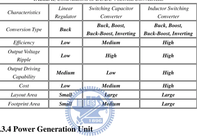
TABLE II. COMPARISONS OF DC/DCVOLTAGE CONVERTERS...26
TABLE III. TFT-LCDDRIVER SYSTEM VOLTAGE SPECIFICATIONS. ...33
TABLE IV. PERFORMANCE COMPARISONS OF VOLTAGE CONVERTERS...74
TABLE V. COMPARISONS OF VOLTAGE CONVERTERS...75
TABLE VI. ICLAYOUT AREA COMPARISONS OF VOLTAGE CONVERTERS. ...84
Chapter 1
Introduction of TFT-LCD Driver
The evolution of thin film transistor-liquid crystal display (TFT-LCD) has four waves [1]. The first wave is the product introduction, making the world flat with the help of TFT-LCD! The application of TFT-LCD ranges from small size hand-held device to TV application from 1990 till now. The second wave is the performance enrichment, making the world gorgeous! The performance of TFT-LCD is getting more colorful, brighter, longer lifetime and faster display speed. The third wave is power and material utilization, making the world green! As the size of the display panel increases, the power consumption becomes much larger. The technology nowadays focuses to lower the power consumption of the TFT-LCD device. The fourth wave is the functions for human interface, making the world without gap! The consumers expect more functions and better performance with the improvement of the human interface technology. As a result, the TFT-LCD becomes the most glory star of the flat display panel (FDP) industry.
This chapter will show the basic topology of the TFT-LCD driver, especially applied to mobile or handheld in section 1.1 firstly. And the main function blocks of the TFT-LCD driver will be showed in section 1.2. The Power Stage, the muscle of the TFT-LCD driver in will be shown in section 1.3. Finally, the power specification of the TFT-LCD driver will be revealed in section 1.4.
1.1 TFT-LCD Driver
As shown in Fig. 1, there are several function blocks in the TFT-LCD driver. These function blocks are realize within a system on chip (SOC) for the sake of power saving and area saving.
All the function block diagrams of the TFT-LCD driver need different power sources. From Fig. 1, the Display Driver IC (DDI) inputs system power VCI into the power generation unit to generate the VCORE voltage for the timing control (TCON), VGH and VGL voltages for the gate driver, DDVDH and VCL voltages for the gamma reference circuit, the common plate voltage (VCOM) reference voltage circuit and the source driver separately. The methods of generating these analogy voltages needed in the TFT-LCD driver will be explained more detail in the later chapter. This work proposes a method to decrease the IC layout area and the number of the external flying capacitors for generating DDVDH and VCL voltages.
G at e D ri ve r Fig. 1. TFT-LCD Driver.
The timing control unit controls all of the timing of the DDI by receiving data signals from the interface input, transfers into the gate driver, the source driver and even the power block control signals.
The gate driver is responsible for the on and off control of the thin film transistor (TFT). By receiving the control signals from the TCON, the gate driver turns on each gate line of the
TFT-LCD panel sequentially.
The source driver is responsible to charge (or discharge) the analogy voltage inside the sub-pixels of the TFT-LCD panel. The gamma reference voltage circuit generates the gamma voltage levels to the source driver. The VCOM reference voltage circuit generates the common plate voltage for the TFT-LCD panel, this voltage may be dc or ac voltage, and normally can be adjusted the voltage value by the registers in the system.
Let’s gain further insight into the relationship between the gate driver, the source driver and the TFT-LCD panel. Fig. 2 is an equivalent circuit of a panel for Quarter Video Graphics Array (QVGA) resolution.
G at e D ri ve r (Sc an D ri ve r/ R ow D ri ve r) P ow er D om a in: V G H /V G L
Fig. 2. Equivalent Circuit of a Panel.
720 source drivers and 320 gate drivers. The RGB means one pixel that includes the red, the green and the blue sub-pixels. The power domain of the source driver (also named data driver or column driver) is DDVDH. The power domain of the gate driver (also named scan driver or row driver) is VGH/VGL.
From Fig. 2, we can see each TFT is responsible for one single sub-pixel LC capacitor. The other G2~320 output VGL voltage when the gate driver G1 outputs VGH voltage. Those
TFTs along G1 direction are turned on. At the same time, source drivers S1~720 output their
own gray scale voltages through each TFT of the sub-pixel that G1 turns on, and store the gray
scale voltage into each sub-pixel LC capacitor before G1 outputs VGL, turning those TFTs
along G1 direction off. And then, as G2 outputs VGH voltage, those TFTs along G2 direction
are turned on. All source drivers S1~720 output the gray scale voltages as well. After that, G2
output VGL, turning off all TFTs. So at this time, the sub-pixels of two gate lines are charged to the desired voltage levels. By this means, G3~320 are turned on or off sequentially,
completing to store all sub-pixels of the TFT-LCD panel in one frame. Frame rate of 60Hz means completing update 60 frames per one second.
1.2 Block Diagram
In this keen competition industry, how to produce the lowest cost without suffer the quality of a product is a big challenge. For the TFT-LCD driver IC vendors, providing with a lower price and less external components can create a win-win situation of both the IC vendors and the module manufacturers. The conventional work uses a dual side method by two flying capacitors to generate DDVDH and VCL separately, but this work proposes a new method with dual side dual output, successfully reduces 4 IC pin outs, 2 flying capacitors and 4 power switches without sacrificing the display quality.
TFT-LCD panel with the resolution of 240RGB*320 dots, comprising 720 channel source drivers, 320 channel gate drivers, 172,800 bytes Graphic Random Access Memory (GRAM) for graphic data of 240RGB*320 dots, and the power supply source generation circuit. This power supply source generation circuit utilizes switching capacitor voltage converters to generate DDVDH, VCL, VGH and VGL voltage for the source driver, the gamma reference circuit, the gate driver and the VCOM reference circuit. Let’s gain more insight into the TFT-LCD driver. 8/9/16/18bit MCU I/F 3/4 Serial I/F 6/16/18bit RGB I/F IOVCC IM[3:0] RESX; DSX WRX; RDX D/CX; EXTC D[17:0]; SDA HSYNC; VSYNC DOTCLK SMX; SMY TEST[9:0] Regulator VCORE DGND
Index Register (IR) Control Register (CR) Graphics Operation Read Latch Write Latch Graphics RAM (GRAM) Address Counter (AC) ENABLE SRGB OSC Timing Controller
Switch Capacitor Voltage Converters (Charge-Pump Voltage Converters) VCI AGND C1 1 P C1 1 N C1 2 P C1 2 N D D VD H C3 1 P C3 1 N C3 2 P C3 2 N VCL C21 P C2 1 N C2 2 P C2 2 N V G H V G L VCOM Reference V CO MH V CO M L LCD Gate Driver VCOM G[320:1] Brightness Control PWM_OUT CABC Gamma Reference Circuit Vreg1out LCD Source Driver S[720:1] DDVDH VCL DDVDH DDVDH VGH VGL
Traditionally: 8 pin outs(C11P,C11N,C12P,C12N,C31P,C31N,C32P,C32N) Proposed: 4 pin outs(C11P,C11N,C12P,C12N)
Fig. 3. TFT-LCD Driver Block Diagrams.
1.2.1 Gate Driver
TFT-LCD gate driver is composed of the shift registers, a level shifter and a digital output buffer. The gate drivers use vertical clock (V_Clock) and vertical synchronize signal (VSYNC) to control the turn on and turn off timing of each gate driver. The level shifters are responsible for change the low dc voltage level of signals to high voltage level VGH/VGL domain. The digital buffers are responsible for the output driving capability of the gate drivers.
Shift register Shift register V_Clock VSYNC Shift register LEVEL SHIFTER Digital Buffer G[320:1] VGH: 10~20V VGL: -5~15V G[1] VGH VGL G[2] G[3]
Fig. 4. TFT-LCD Gate Driver.
As in Fig. 4, the gate drivers output VGH or VGL voltage to control the on or off state of these TFT arrays. Different TFT-LCD panels possess different I-V curves of the thin-film transistors. So the switching capacitor converter generating VGH and VGL voltage should keep the elasticity of different voltage level settings.
A QVGA resolution the TFT-LCD panel comprises 240RGB*320 dots. A gate driver G[1] outputs voltage VGH to turn on the TFT array of G[1], then all source drivers S[720:1] begin
to charge each sub-pixels to the gamma voltage levels being set individually. After all the sub-pixels finish the charging action, the gate driver G[1] outputs voltage VGL to turn off the TFT array of G[1].
And then gate driver G[2] outputs voltage VGH to turn on the TFT array of G[2], then all source drivers S[720:1] begin to charge each sub-pixels to the gamma voltage levels being set individually. After all the sub-pixels finish the charging action, the gate driver G[2] outputs voltage VGL to turn off the TFT array of G[2].
Following this rule, after the last gate driver G[320] finishes this action, a frame picture is written and displayed on the TFT-LCD panel. Frame rate 60Hz means the TFT-LCD driver updates 60 frame data per one second.
1.2.2 Gamma Voltage Generator
Vreg1out is an important power source in the TFT-LCD driver. It plays the role of a power source of the gamma voltage generator circuit. Fig. 5 shows a linear regulator that produces a voltage power Vreg1out. This regulator would adopt a cap-free [12] design in some low cost solution projects.
This linear regulator is composed of a VREFGEN circuit, an error amplifier, a pass element and a feedback network. The VREFGEN circuit provides various reference voltage levels. As to the error amplifier, it amplifies the error amount of the reference voltage and the feedback voltage. After receiving the amplified error voltage, the pass element of Vreg1out regulator as a PMOS, adjusts the output Vreg1out voltage to a suitable level. Finally is the feedback network, comprising of resisters, is responsible for providing the weight of Vreg1out as the feedback voltage.
In real case application, Vreg1out power source should keep the elasticity of a wide voltage range as Fig. 5 showed. We can count on the registers VRH[5:0] to select the exact
reference voltage levels from the VREFGEN circuit for the Vreg1out regulator. VREF GEN VRH[5:0] OP DDVDH: 4.7~6V Vreg1out: 3~5.5V Stablize Capacitor
Fig. 5. Vreg1out regulator: Reference Power of Gamma Voltage Generator.
The simplest distinction of brightness and darkness is binary level. It means just only bright and dark. For a RGB sub-pixel display, if all RGB sub-pixels only exists two states of bright and dark state, the display color depth equals to 2 bits. That is to say, the panels can only display 8 kinds of color. In the real world, even mono color such as black, exists different gray levels. And each gray level exhibits a different shading value to human eyes. In order to realize the nature images seen by the human eyes, the need of gray levels is necessary.
This work utilizes 6 bits color depth. That means R or G or B color exists 64 gray levels individually. That is to say, the TFT-LCD driver can display 262,144 kinds of color on the TFT-LCD panel.
In Fig. 6, we can realize that the Gamma Voltage Generator circuit is used to generate 64 gray levels of voltage for 6 bits color depth.
Vreg1out G A M M A O P M U X GAMMA[63:0] DDVDH: 4.7~6V
Fig. 6. Gamma Voltage Generator.
The generator circuit comprises a resister type voltage divider, a mux, and the gamma operation amplifiers. The resister type voltage divider uses Vreg1out as a reference power source, and divides various sets of reference voltage as the reference voltage of the gamma operation amplifiers. The mux circuits select the relative reference voltage by the registers for the gamma operation amplifiers. The gamma operation amplifier always configures as an unity gain topology and plays the role of an analogy output buffer of the 64 gray levels.
The liquid crystal is a kind of a light gate. The transmitted luminance depends on the rotate angle of the liquid crystal molecules controlled by the voltage applied across the top
plate and bottom plate of the TFT-LCD panel. As in Fig. 7, the LC voltage means the voltage applied across the TFT-LCD panel. Each voltage level relates to different transmitted luminance.
An opposite sign of the LC voltage results in an opposite rotate angle, but however, relates to the same transmitted luminance. We will introduce in the later section. This is what the polarity change method does. The polarity change method must be applied to increase the lifetime of a TFT-LCD panel and prevents it from dc residue effect.
Transmitted Luminance (%)
LC Voltage
V
0 +V
1 +V
63 +V
0-V
1-V
63 -0
100
Fig. 7. LC Gamma Curve.
1.2.3 Source Driver
capacitors and liquid crystal capacitors of a TFT array on a TFT-LCD panel, which is turned on by the selected gate driver. For a resolution of QVGA 240RGB*320, the source drivers S[720:1] need to charge 320 sub-pixels individually and sequentially to complete one single frame data. For 60 Hz frame rate, the source drivers need to drive 60 frame data in one second.
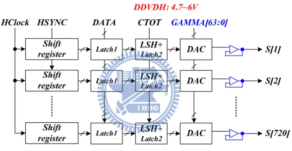
In Fig. 8, the TFT-LCD source drivers [2] are composed of the shift registers, the latches, the level shifters, the DACs (digital to analogy converter) and the source operation amplifiers.
Fig. 8. TFT-LCD Source Driver.
The display DATA are latched in latch1 through the shared 18 bits data bus. The source drivers use HClock (horizontal clock signal) and HSYNC (horizontal synchronize signal) to control the shifter registers to store the display DATA sequentially into each latch1 of the source drivers. Then the display DATA are stored into the latch2 and the level shifter by the CTOT signal. The CTOT signal is a signal similar to the HSYNC signal. After that, the display DATA select the desired gamma gray level voltages by DAC circuit, and at last, the source operation amplifiers which are configured as analogy unity gain output buffers, are
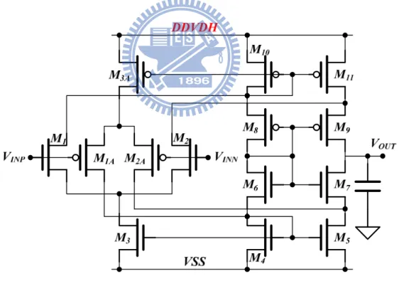
responsible for driving the desired gamma gray level voltages into the selected sub-pixels. Fig. 9 shows a self-biased folded cascode rail-to-rail operation amplifier [13]. The source op-amplifiers are used to drive 64 gamma gray scale voltage levels into the TFT-LCD panel. The op-amplifiers should be able to drive signals range within full range from DDVDH to ground because of the voltage range of 64 gamma gray scale voltage levels are almost full range from DDVDH to ground. For a QVGA resolution with 240RGB*320, there must exist 720 source drivers which contain 720 source op-amplifiers. The total dc static operation current for source op-amplifiers is very large if we use the conventional two-stage op-amplifier. A Self-biased and class AB folded cascode op-amplifier is a very suitable solution to the source drivers.
Fig. 9. Self-biased Folded Cascode Rail-to-rail Op-amplifier.
1.2.4 Data Driving Method
TFT-LCD driver first. The liquid crystal acts like the light gate, controlled by the voltage across it, to adjust the angle of the liquid crystals, resulting in brightness control. Unlike the spontaneous light emitting display panel, the TFT-LCD panel need extra backlight source such as Cold Cathode Fluorescent Light (CCFL) or Light Emitting Diode (LED) to display a picture.
The electric field applied to the liquid crystals is oriented. If we change the electric field with an opposite direction, that is so-called polarity change [2]. This polarity change would not and should not result in the transmitted luminance of the liquid crystals, but the angles of them. Because the DC blocking effect of the orientation layer and the dc residue effect of TFT-LCD panel, we must apply polarity change by line or by frame.
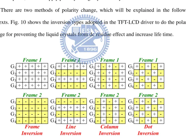
There are two methods of polarity change, which will be explained in the following contexts. Fig. 10 shows the inversion types adopted in the TFT-LCD driver to do the polarity change for preventing the liquid crystals from dc residue effect and increase life time.
Fig. 10. Inversion Types of TFT-LCD Driver.
Frame inversion updates the pixel voltage polarity in the form of frame. We can see all of the sub-pixels in frame 1 are positive, and in frame 2 are negative.
direction). We can see in frame 1, the sub-pixels of GODD are positive and those of GEVEN are
negative. But in frame 2, the sub-pixels of GODD are negative and those of GEVEN are positive.
Column inversion updates the pixel voltage polarity in the form of column. We can see in frame 1, the sub-pixels of SODD are positive and those of SEVEN are negative. But in frame 2,
the sub-pixels of SODD are negative and those of SEVEN are positive.
Dot inversion updates the pixel voltage polarity in the form of pixel. We can see in frame 1, all of the polarity of the sub-pixel is contrary to the neighbor ones. And in frame 2, all of the polarity of the sub-pixel change.
AC VCOM Data Driving Method
VCOM voltage is a reference common electro plate voltage inside the panel. AC VCOM means the VCOM voltage level changes polarity by line or by frame to avoid the dc residue effect of the liquid crystals. In Fig. 11, VCOM voltage changes polarity by line or by frame between the voltage level VCOMH and VCOML. The VCOMH and VCOML voltage depend on the LC characteristics for the different panel makers.
In the positive polarity period, the voltages across the liquid crystals are gray scale voltages (V0+ ~ V63+) minus VCOML, these voltages are the positive sign voltages, and then,
in the negative polarity period, the voltages across the liquid crystals are gray scale voltages (V0+ ~ V63+) minus VCOMH, these voltages are the negative sign voltages.
If we well adjust VCOMH and VCOML voltage level to let the positive sign voltage just equal to the absolute value of the negative sign voltage, by doing so can prevent the liquid crystals from dc voltage residue and increase their life time.
AC VCOM Driving Method V0 + V1+ V62 + V63 + V63 -V62 -V1 -V0 -Gray Scale Voltage VCOM waveform VCOMH VCOML
Positive Polarity Negative Polarity
1 line/frame
Fig. 11. AC VCOM Driving Method.
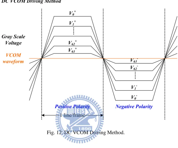
DC VCOM Data Driving Method
Fig. 12 shows the DC VCOM driving method. DC VCOM means the VCOM voltage level always keeps a dc value at anytime. By this way, the job of polarity change is controlled only by the source drivers.
In the positive polarity period, the voltages across the liquid crystals are gray scales voltage (V0+ ~ V63+) minus VCOM, these voltages are the positive sign voltages, and then, in
the negative polarity period, the voltages across the liquid crystals are gray scale voltages (V0+
~ V63+) minus VCOM, these voltages are the negative sign voltages.
If we well adjust VCOM voltage level to let the positive sign voltage just equal to the absolute value of the negative sign voltage, by doing so can prevent the liquid crystals from dc voltage residue and increase their life time. But different from the AC VCOM, the gray scale voltages range (V0+ ~ V63+) of the DC VCOM method must large than the AC VCOM to
maintain the same voltage levels across the liquid crystals.
DC VCOM Driving Method V0 + V1 + V62 + V63 + V63 -V62 -V1 -V0 -Gray Scale Voltage VCOM waveform
Positive Polarity Negative Polarity
1 line/frame
Fig. 12. DC VCOM Driving Method.
Comparison Between AC VCOM and DC VCOM
TABLE I. shows the advantages and disadvantages comparisons of AC VCOM and DC VCOM. Let’s gain further insight into the differences between the AC VCOM and the DC VCOM data driving method.
For example, in AC VCOM case, assume Gray scale voltage V0+ =4V
Gray scale voltage V0− =0.5V
VCOML voltage VCOML=−0.5V
VCOMH voltage VCOMH =5V
In the positive polarity, the voltage across the liquid crystal is 4.5V, and in the negative polarity, the voltage across the liquid crystal is -4.5V. Because the Gray scale voltage range is 4V to 0.5V, the source driver only need the 5V device for this design.
In DC VCOM case, assume Gray scale voltage V0+ =4V
Gray scale voltage V0− =−5V
VCOM voltage VCOM =−0.5V
(2)
In the positive polarity, the voltage across the liquid crystal is 4.5V, and in the negative polarity, the voltage across the liquid crystal is -4.5V. Because the Gray scale voltage range is 4V to -5V, the 5V device can not meet this design in the source driver. In this case, the source driver needs the 12V device and this will increase the wafer cost.
In TABLE I, the image quality of DC VCOM is better than AC VCOM, but the cost of DC VCOM is more than AC VCOM because the higher voltage process is needed. This work uses AC VCOM for design because the cost of AC VCOM is lower than DC VCOM.
TABLE I. COMPARISONS OF DATA DRIVING METHODS
Characteristics AC VCOM DC VCOM
Inversion Type Frame, Line inversion
Frame, Line, Column,
Dot inversion
Image quality Poor Better
Power dissipation Higher Lower
Process Lower voltage process Higher voltage process
1.2.5 VCOM Driver
The liquid crystals of the sub-pixel, as a light gate of TFT-LCD panel can be regarded as a capacitor with two parallel electrode plates. Inside a sub-pixel of TFT-LCD panel, one of the electrode plates is isolated individually with the other sub-pixels, connects to the thin film transistor and expands to two-dimensional arrays together with all the other sub-pixels. Another electrode plate of the sub-pixel, named as VCOM (the common electrode plate) is actually shared with all sub-pixels of the panel. The VCOM voltage level plays the role of the reference voltage of all liquid crystals of a TFT-LCD panel. We can change the VCOM voltage level to eliminate the flicker effect of a TFT-LCD panel [14]. The voltage difference across the two plates of a sub-pixel is direct proportional to the electric field intensity be applied to the liquid crystal, and is also proportional to the transmitted luminance of the liquid crystal.
The VCOM driver is used to provide the reference common electrode plate voltage of the TFT-LCD panel. As mentioned in the last section, there are two methods to fulfil the liquid crystal polarity change in LCD driving. The liquid crystal polarity change is responsible for increasing the lifetime of the liquid crystal, and also preventing the liquid crystal from the dc residue effect. This work utilizes AC VCOM driving method for polarity change.
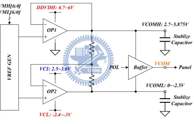
Fig. 13 shows the structure of the VCOM driver. The VCOM driver is composed of a reference voltage generation circuit, two operation amplifiers and an analogy output buffer.
The reference voltage generation circuit is responsible for providing the reference voltages for VCOMH and VCOML, controlled by VMH[6:0] and VML[6:0] registers. OP1 is a p-type (PMOS as input device) folded cascode operation amplifier, generates VCOMH voltage for the VCOM driver. OP1 uses DDVDH and VSS as power and ground because of the VCOMH voltage specification range is between 2.7V to 5.875V. OP2 is a n-type (NMOS
as the input device) folded cascode operation amplifier, generates VCOML voltage for the VCOM driver. OP2 uses VCI and VCL as power and ground because of the VCOML voltage specification range is between 0V to -2.5V. At last, the analogy buffer is responsible for output the AC VCOM voltage level into the TFT-LCD panel. The POL (polarity) signal is used to control the analogy buffer to output the VCOMH voltage level when the POL signal at high level, and when the POL signal is at low level, the analogy buffer outputs the VCOML voltage level. V R E F G E N
Fig. 13. TFT-LCD VCOM Driver.
1.3 Power Stage Selection
In Fig. 14 [3], in a cell phone module system, the system power supply comes from the battery. Function blocks such as PA (power amplifier), LNA (low noise amplifier), Analogy R/F (radio frequency), Baseband, Display (TFT-LCD), Audio and Interface, need different power supply sources. And there are 4 choices of power supply: 1) nothing, directly from
battery, 2) LDO, 3) switching capacitor, 4) inductor switching regulator. Baseband Charger Battery PS LNA PA Antenna PS D/A A/D LO Analog R/F 2.7~5.5V 2.5V PS 2.5V µP/DSP core I/O PS 1.5V PS 2.5V Interface Audio PS 1.65~3.6V PS 2.5~3.6V Display PS VBAT=2.7~5.5V
PS Power supply choices: 1) nothing 2) LDO
3) switching capacitor 4) inductor switching regulator
(VCI) (IOVCC)
Fig. 14. Power supply of Cell Phone System.
Based on the functions and the power consumption budgets, every power supply sources may have different choices.
1.3.1 Linear Regulator
Linear Regulator as Fig. 15 [4] shown, is composed of a reference voltage circuit, an error amp, a pass element and a feedback element. Early days architectures need an extra stabilize capacitor, but nowadays, many new proposed architectures with multi-stage design, miller compensation, and nested miller compensation had been accomplished cap-free design [12].
Reference voltage Error Amp VIN VOUT Stablize Capacitor Pass Elements VREF VFB
Fig. 15. Linear Regulator.
The advantages of the linear regulator: circuit structure simple, low cost, low footprint area, low output voltage ripple, fast line response time and fast load response time.
The disadvantage of the linear regulator: can only generate output voltage lower than input voltage, lower efficiency when the voltage drop between the input voltage and the output voltage increase and thermal dissipation large.
The reference voltage circuit is used to generate a reference voltage that is independent of process, voltage and temperature.
The error amp is an error operation amplifier that amplifies the error voltage between the reference voltage VREF and the feedback voltage VFB for controlling the pass elements. For the
system stability consideration, an error amp usually applies some ac compensation method. Normally if an error amp with large dc gain, the accuracy of output voltage will be better.
or PMOS). The choices of pass elements are often depend on the application, specification and cost. Pass elements maybe external discrete components or built-in SOC devices.
The feedback element is often composed of a resistor network, sometimes may need extra capacitors for ac compensation. The main job of a feedback element is to generate feedback voltage for error amp.
1.3.2 Switching Capacitor Converter
Fig. 16 is a typical voltage doubler of switching capacitor converter [5] [6]. A switching capacitor converter can generate an output voltage larger (boost) or smaller (buck) than the input voltage, and even more, a negative voltage.
In many applications, the boosted voltage or the bucked voltage or even the buck-boost voltage are needed in the system, but when the footprint area or the cost are issue, switching capacitor converter is a practical solution. Handheld or mobile application often chooses this method as a solution, this work (TFT-LCD Driver) is a good example.
V
INC
1C
2i
INL
O
A
D
I
OUTV
OUT= 2·V
INS
1S
2S
3S
4charge
pump
Fig. 16. Switching Capacitor Converter: Voltage Doubler.
medium cost.
The disadvantages of switching capacitor converter: output driving capability small, output ripple high, layout area large.
Generally speaking, the switching capacitor converters, also named the charge pumps, are composed of the power switches and the capacitors. As shown in Fig. 16, there are two phase timing for the voltage doubler operation. During the charge phase, switch S1 and S2 are
closed, but S3 and S4 are opened. Top plate of the capacitor C1 is charged to VIN by S1 and
bottom plate of it is charged to GND by S2. During the pump phase, switch S1 and S2 are
opened, but S3 and S4 are closed. Bottom plate of the capacitor C1 is charged to VIN by S3 and
because the charge conservation theorem, the top plate of C1 is now 2·VIN, and be connected
to VOUT by S4. After several repeated operations of charge and pump phase, VOUT will
generally increases to 2·VIN. The following chapter will have more detail descriptions of the
switching capacitor voltage converter.
1.3.3 Inductor Switching Converter
This type of voltage converter needs at least one inductor as an electric energy storage component. Compared with the linear regulator and the switching capacitor converter, the inductor switching converter provides highest efficiency. A higher efficiency can minimize thermal dissipation issue, and also increases lifetime of the battery in the handheld or the mobile application. Besides, inductor switching converters also support inverting (negative voltage), buck (lower voltage than input), boost (higher voltage than input), and even buck-boost topology [7].
The Inductor switching converters usually apply the pulse width modulation (PWM) by changing the duty cycle to control the on/off of Power MOSFET. By doing so, we can change the amount of the electric energy stored inside the inductor to control the output voltage. The
RDSON (on resistance) of the Power N-MOSFET lower, the power loss will be smaller,
resulting in higher power conversion efficiency. However, when the output current loading becomes smaller, the efficiency of the PWM control method will lower. This is because the switching loss dominates at small output current. Some control mechanisms such as pulse frequency modulation (PFM) [8] or pulse skipping modulation (PSM) [9] will have better efficiency at the smaller output current loading condition by reducing the operation frequency or skipping some on pulses to minimize the switching loss.
The advantages of inductor switching converter: highest conversion efficiency and large output driving capability.
The disadvantages of inductor switching converter: high cost, complex design, large output voltage ripple, large layout area and EMI issue.
Fig. 17 shows the asyncronize boost type of the inductor switching converter [10]. This converter is composed mainly by a driver circuit, a feedback network and an inductor L1, a
Power NMOS T1 and a diode D1. In the synchronize boost design, D1 will be replaced by a
Power PMOS. L O AD Fe e d b a c k N e two rk
Fig. 17. Inductor Switching Converter: Boost.
reference voltage and the feedback voltage and a PWM generation circuit, which turns the amplified error voltage into a PWM signal, then modulates the duty cycle of the Power NMOS T1. The feedback network is responsible for monitor the output voltage and returns a feedback voltage, and even in a current mode operation, it will returns an output current loading information to the control driver circuit.
The operation theory of a boost inductor switching converter is as below:
First, the Power NMOS T1 turns on, the drain of T1 equals almost to ground, D1 is
reverse biased and turns off, then the input voltage VIN stores energy into the inductor L1 and
the inductor current ramps up and the capacitor CL supplies current to output load. Assuming
the RDSON of the Power NMOS is very small to be ignored,
Increased inductor current IN ON
L T
L V I (+)= −0
∆ (3)
Second, the Power NMOS T1 turns off, the drain of T1 equals to VIN, D1 is forward
biased and turns on, then the energy stored in the inductor L1 begins to discharge through D1
toward VOUT, and the inductor current ramps down. Assuming the forward voltage of D1 is
small enough to be ignored,
Decreased inductor current OUT IN OFF
L T L V V I − = − ∆ ( ) (4)
Since the inductor current can not be changed abruptly, Eq. 3, must equals to Eq. 4.
OFF OFF ON IN OFF ON IN OUT T T T V T T V V = (1+ )= + (5) OFF ON S T T T = + , S ON T T D= , S OFF T T D = − ) 1 ( (6)
After replacing Eq. 6 into Eq. 5, we can derive the relation of VOUT and VIN,
D V
V IN
OUT = −
1 (7)
From Eq. 7, 0< D<1, so the output voltage VOUT must be larger than the input voltage VIN. This is why we call the boost type inductor switching converter because it can generate a
Table II shows the comparison of the linear regulator, the switching capacitor converter, and the inductor switching converter.
1.3.4 Power Generation Unit
After comprehending sections 1.3.1 to 1.3.3, let’s move into the power generation unit of the TFT-LCD driver. As shown in Fig. 14, the power supply system of a cell phone provides two power sources to the TFT-LCD driver. That is, the power source, VCI, is the main analogy system power and the other power source, IOVCC, is the I/O (input/output pad) interface power as depicted in Fig. 18, the power generation unit of the TFT-LCD driver.
VCORE voltage ranges from 1.6V to 1.9V, generated by LDO and is responsible for the TCON and the SRAM power. This voltage is always determined by the low voltage device of the silicon process.
DDVDH voltage ranges from 4.7V to 6.0V, generated by charge pump and is responsible for the power of the source driver and the VCOM driver. This voltage is always determined by the characteristics of the liquid crystals for the different panel makers.
TABLE II. COMPARISONS OF DC/DCVOLTAGE CONVERTERS
Characteristics Linear Regulator Switching Capacitor Converter Inductor Switching Converter
Conversion Type Buck Buck, Boost,
Buck-Boost, Inverting
Buck, Boost, Buck-Boost, Inverting
Efficiency Low Medium High
Output Voltage
Ripple Low High High
Output Driving
Capability Medium Low High
Cost Low Medium High
Layout Area Small Large Large
VCL voltage ranges from -2.4V to -3V, generated by charge pump and is responsible for the VCOM driver’s power. This voltage is also determined by the characteristics of the liquid crystals for the different panel makers.
Fig. 18. Power Generation Unit of TFT-LCD Driver.
VGH voltage ranges from 10V to 20V, generated by charge pump and is responsible for the gate driver’s power. This voltage is always determined by the characteristics of the TFTs for the different panel makers.
VGL voltage ranges from -5V to -15V, generated by charge pump and is also responsible for the gate driver’s power. This voltage is also determined by the characteristics of the TFTs
for the different panel makers.
Vreg1out voltage ranges from 3.0V to 5.5V, generated by LDO and is responsible for the reference power of the gamma voltage generator. This voltage is always determined by the characteristics of the liquid crystals for the different panel makers.
VCOMH voltage ranges from 2.7V to 5.875V, generated by LDO and is responsible for the VCOM driver’s power. This voltage is always determined by the characteristics of the liquid crystals for the different panel makers.
VCOML voltage ranges from 0V to -2.5V, generated by LDO and is responsible for the VCOM driver’s power. This voltage is also determined by the characteristics of the liquid crystals for the different panel makers.
From Fig. 18 and Fig. 19, the DDVDH voltage is generated by charge pump (CP1) with
two flying capacitors (C11, C12).
The charge pump (CP1) with two flying capacitors is a so-called dual side charge pump.
A dual side charge pump can reduce the voltage ripple by the dual side operation [11].
VCL is generated by charge pump (CP4) with two flying capacitors (C31, C32). This is
also a dual side charge pump.
VGH and VGL are generated by charge pump (CP23) with two flying capacitors (C21,
C22). This charge pump is not a dual side charge pump because the two flying capacitors are
needed to generate higher level voltage of VGH and VGL as shown in Fig. 19.
This work proposes a new voltage converter using only two flying capacitors to generate DDVDH and VCL power sources, saving the footprint area by reducing the number of the external flying capacitors, and at the same time, saving the layout area by reducing the IC pin outs and the number of the power switches. Later chapter will have more detail contents for it.
Fig. 19. Simple Operation Principle of CP1, CP4 and CP23 in TFT-LCD Driver.
1.4 Power Specification
The power management unit is a very important function block in every different application integrated circuits. Fig. 18 showed the TFT-LCD driver’s power generation unit that is composed of various types of linear regulators and switching capacitor converters. Let us review the power budgets of every function blocks of this work. For a QVGA 240RGB*320 resolution, frame rate 60Hz, the inversion types chooses line inversion as the worst case:
Source driver power consumption: Based on the regular source panel loading ranges from 10pF to 20pF, the source driver output voltage changes from 0.5V to 4.5V.
mA p
VCOM driver power consumption: Based on the regular VCOM panel loading ranges from 5nF to 15nF, the VCOM driver output voltage changes from 4V to -1V.
mA n IDDVDH VCOM 320) 60 15 [4 ( 1)] 0.72 2 1 ( _ = ⋅ ⋅ ⋅ ⋅ − − = mA n IVCL VCOM 320) 60 15 [4 ( 1)] 0.72 2 1 ( _ = ⋅ ⋅ ⋅ ⋅ − − = (9)
Gate driver power consumption: Based on the regular gate panel loading ranges from 20pF to 40pF, the gate driver output voltage changes from 15V to -10V.
uA p IVGH_GATE =320⋅60⋅40 ⋅[15−(−10)]=19.2 uA p IVGL_GATE =320⋅60⋅40 ⋅[15−(−10)]=19.2 (10)
TCON and SRAM power consumption: This item varies with process and various digital functions and typically 1mA to 2mA current budget comes from the VCORE linear regulator.
Vreg1out power consumption: Vreg1out is the reference power of the gamma resistors, normally consumes current less than 50uA, this current comes from DDVDH.
VCOMH power consumption: As Eq. 9 showed, the average current consumption of VCOMH is 0.72mA and this current comes from DDVDH.
VCOML power consumption: As Eq. 9 showed, the average current consumption of VCOML is 0.72mA and this current comes from VCL.
Let’s summarize the current budgets as follow:
DDVDH is generated by CP1 and the current budget is:
mA m
m m
IDDVDH_total =1.106 +0.72 +0.05 =1.876 (11) VCL is generated by CP4 and the current budget is:
mA
IVCL_total =0.72 (12)
VGH and VGL is generated by CP23 and the current budget is:
uA
uA IVGL_total =19.2
In Fig. 20, the conventional dual side CP1 use two flying capacitors to generate DDVDH,
and the conventional dual side CP4 use two flying capacitors to generate VCL, too. This work
proposes a new dual side dual output CP14 as Fig. 20 shows that uses only two flying
capacitors to generate DDVDH and VCL.
Fig. 20. New Proposed Dual Side Dual Output Charge Pump
The new proposed method saves two flying capacitors, 4 pin outs and 4 power switches for generating DDVDH and VCL. The IC layout area of the new proposed method saves more than 27% than the traditional method without sacrificing the display quality.
introduced in section 1.2, the source driver, the Vreg1out regulator, the VCOMH and the VCOML generator use op-based structure to achieve high line regulation performance.
The source drivers are responsible for driving 64 gamma gray levels into the TFT-LCD panel. The voltage steps between each gamma gray levels are not equal because of the gamma correlation of the human eyes. The minimum gamma voltage step is around 15mV and that means if the voltage difference is smaller than 15mV, the human eyes may not be able to recognize the difference of the gamma level. The line regulation of source driver is 0.74mV/V in DDVDH power domain and that means if DDVDH voltage changes abruptly 20.27V, the source driver output voltage will change 15mV. We can figure out if DDVDH voltage changes abruptly 33.33V, the output voltage of Vreg1out regulator will change one step 50mV. Also if DDVDH voltage changes abruptly 7.35V, the output voltage of VCOMH will change one step 25mV. We can come out a summary for DDVDH voltage that the voltage ripple of DDVDH should be smaller than 7.35V to meet the specifications of the source driver, the Vreg1out regulator and the VCOMH voltage generator.
We can also figure out that if VCL voltage changes abruptly 3.65V, the output voltage of VCOML will change one step 25mV. So VCL voltage ripple should be smaller than 3.65V to meet the specification of the VCOML voltage generator.
All of these voltage specifications are listed in TABLE III. From Table III, we can get the maximum output impedance specifications for DDVDH and VCL,
Ω = − ⋅ = − ⋅ =(2 )/ _ (2 2.5 4.7)/2 150 _ _ VCI DDVDH I mA
ROUT DDVDH MAX MIN MIN DDVDH MAX
Ω = ⋅ − − − = ⋅ − − =[ ( 1) ]/ _ [ 2.4 ( 1) 2.5]/0.8 125 _ _ VCL VCI I mA
ROUT VCL MAX MAX MIN VCL MAX
TABLE III. TFT-LCDDRIVER SYSTEM VOLTAGE SPECIFICATIONS.
Line Regulation Voltage Spec
Source driver 0.74 mV/V (DDVDH) Gamma step Min 15mV
Vreg1out 1.5mV/V (DDVDH) Vreg1out 3.0V~6.0V, step 50mV
VCOMH 3.4mV/V (DDVDH) VCOMH 2.7V~5.875V, step 25mV
VCOML 6.85mV/V (VCL) VCOML -2.5V~0V, step 25mV
Power Spec
VCI 2.5V~3.6V
DDVDH 4.7V~6.0V, ripple < 1V, max current 2mA ROUT_DDVDH_MAX=150ΩΩΩΩ
VCL -2.4V~-3V, ripple < 1V, max current 0.8mA ROUT_VCL_MAX=125ΩΩΩΩ
VGH 10V~20V, max current 25uA
Chapter 2
Performance Checking of Switching
Capacitor Voltage Converter
With the progress of semiconductor process from submicron meter to deep submicron meter such as 0.35um, 0.25um, 0.18um, 0.13um and even 45nm, the devices are made smaller generation by generation, and the power supply voltage levels for the smaller devices also drop generation by generation for solving power dissipation issues. But some special application ICs such as the electrically erasable programmable read-only memory (EEPROM), the flash memories, the dynamic random access memory (DRAM) and the TFT-LCD drivers need high voltages for normal function operation. Charge pumps have been used to generate voltages higher than the system power supply voltage for these applications. Charge pumps characterized with low EMI (electro magnetic interference), inductor-less, high efficiency larger than 90%, low cost, low profile and compact are often the best choice of the handheld TFT-LCD drivers. The charge pumps have many different topologies [15] [16] [17]. In this chapter, we will introduce the voltage doubler and the voltage inverter. Gaining more insight into the theory of the charge pump is the goal of this chapter. Section 2.1 introduces some basic concepts about the switching capacitor [18], section 2.2 shows the voltage doubler converter and at last, section 2.3 explains the theories of the voltage inverter converter.
2.1 Basic Concepts about Switching Capacitor
2.1.1 Charge Transfer of Capacitors
Capacitors are energy storage materials. The energy is stored in the capacitor in the form of electric charge. From the formula of below, if a capacitor with capacitance C1 is charged to
a voltage VIN, then the charge Q1 stored in the capacitor is given by t I V C Q1 = 1⋅ IN = IN ⋅ (14)
In Fig. 21, for the ideal case, the charge Q1 is stored in the capacitor instantaneously, and
that means t approaches zero. From Eq. 14, if t approaches zero, the charging current IIN
approaches infinity.
∞
→
PEAKI
0
→
t
Fig. 21.Waveforms of Charging a Capacitor.
But in real case, the capacitors have the equivalent series resistance (ESR) and the equivalent series inductance (ESL); meanwhile, the power switch has an intrinsic resistance RSW. These resistances and inductance will not only result in energy loss when storing energy
in the capacitor but also increase the time of storing the energy in the capacitor. In other words, the charging current IIN will be suppress to a limited value instead of infinity.
From the law of charge conservation, if two capacitors C1 and C2 with voltage V1 and V2
are connected together, the charge Q1 of C1 and Q2 of C2 will re-distribute between these two
capacitors, but the total charge QT will be,
EQ T Q Q CV C V C C V
Q = 1+ 2 = 1 1+ 2 2 =( 1+ 2) (15) Then the equivalent voltage of the parallel capacitors will be,
2 2 1 2 1 2 1 1 2 1 2 2 1 1 2 1 V C C C V C C C C C V C V C C C Q V T EQ + = + + + + = + = (16)
2.1.2 Switching Capacitor Principle
Fig. 22 shows a simple switching capacitor voltage converter circuit.
L
OA
D
Fig. 22.Waveforms of Switching Capacitor Operation.
The simple switching capacitor circuit composing of two switches S1, S2 and two
be charged to VIN. When S1 is opened and S2 is closed, then C1 is connected to C2, and the
charge of C1 and C2 will re-distribute between each other. Assuming the initial charge of C2 is
zero and the capacitance of C1 and C2 are equal. In phase1, C1 is charged to VIN, and in
phase2, the charge of C1 and C2 re-distribute,
IN IN OUT V C C C V C C C V 2 1 0 2 1 2 2 1 1 = + + + = (17)
After the first cycle, VOUT = (1/2)·VIN, then VOUT = (1/2)·VIN+(1/4)·VIN = (3/4)·VIN after the second cycle. It’s not hard to understand that after infinite cycles, VOUT will approach VIN
very closely.
In the steady state, assuming the switching frequency in Fig. 22 is f. The charge being transferred of each cycle is C1·(VIN-VOUT) and results in an average current,
EQ OUT IN OUT IN OUT IN avg R V V fC V V V V fC I = − = − = − 1 1( ) 1 (18) 1 1 fC REQ = (19)
From Eq. 18 and 19, the switching operation results in an additional equivalent resistance REQ connecting VIN and VOUT. This equivalent resistance leads to an extra power
loss beyond the switch resistances and ESR resistance of capacitors.
2.2 Voltage Doubler
The voltage doubler plays a role of generating the DDVDH voltage of 2 times the system power VCI. As Fig. 1 shown, DDVDH is the power supply for the source drivers, the gamma voltage generator and the VCOM driver in the TFT-LCD driver. This voltage is always determined by the characteristics of the liquid crystals for the different panel makers.
2.2.1 Operation of Voltage Doubler
Reminds we had introduced the operation principle of voltage doubler in section 1.3.2, Fig. 16 shown the circuit of the voltage doubler. The capacitor C1 is the pump capacitor, also
named the flying capacitor, and the capacitor C2 is the load capacitor, also named the stabilize
capacitor.
One complete operation cycle of the switching capacitor converter contains charge phase (phase1) and pump phase (phase2). As we discussed before, there are many energy loss such as the switch resistances, ESR and ESL, and with these resistances the charge or discharge of capacitors need some time.
Assuming the charge pump is at the steady state. During the charge phase (phase1), switches S1 and S2 are closed, S3 and S4 are opened. At this time, C1 is charged to VIN, the
top and bottom plate of C1 is connected to VIN and ground individually in order to store
energy. During the pump phase (phase2), switches S1 and S2 are opened, S3 and S4 are closed.
At this time, C1 transfers energy to C2, the top and bottom plate of C1 is connected to VOUT
and VIN individually. The voltage drop of C1 equals to VIN because the voltage drop of a
capacitor can not change instantaneously. So when S3 is closed, the voltage of C1’s bottom
plate equals to VIN and the voltage of C1’s top plate connected to VOUT by S4 equals to 2VIN.
2.2.2 Voltage Ripple of Voltage Doubler
Fig. 23 shows the steady state waveforms of the voltage doubler. Assuming the output load current is IOUT. The average value of input current iIN is equal to 2IOUT.
A charging current around 2IOUT flows when the flying capacitor C1 is connected to the
input VIN. The initial value of this charging current depends on the initial voltage across C1,
the ESRC1 which is the ESR resistance of C1, and the resistances of the power switches.


![Fig. 16 is a typical voltage doubler of switching capacitor converter [5] [6]. A switching capacitor converter can generate an output voltage larger (boost) or smaller (buck) than the input voltage, and even more, a negative voltage](https://thumb-ap.123doks.com/thumbv2/9libinfo/8460849.183166/33.892.218.702.749.1019/switching-capacitor-converter-switching-capacitor-converter-generate-negative.webp)
![Fig. 17 shows the asyncronize boost type of the inductor switching converter [10]. This converter is composed mainly by a driver circuit, a feedback network and an inductor L 1 , a Power NMOS T 1 and a diode D 1](https://thumb-ap.123doks.com/thumbv2/9libinfo/8460849.183166/35.892.145.787.504.1030/asyncronize-inductor-switching-converter-converter-composed-feedback-inductor.webp)