A Wide Operation Range CMOS Frequency Divider for 60GHz
Dual-Conversion Receiver
Yi-Jan Emery Chen, Shuen-Yin Bai, Tang-Nian Luo, Yueh-Hua Yu, and Deukhyoun Heo*
Graduate Institute of Electronics Engineering, Department of Electrical Engineering
National Taiwan University, Taipei, Taiwan
* School of Electrical Engineering and Computer Science
Washington State University, Pullman, WA 99164 , USA
Abstract — This paper presents a wide operation range
0.18Pm CMOS frequency divider for 60GHz wireless
applications. The direct injection lock technique is used to perform the signal division at millimeter-wave frequency. The deep n-well is implemented under the NMOS switch transistor to improve the lock range of the frequency divider. Combined with band switching and analog frequency tuning, the operation range of the frequency divider covers from 43 to 49 GHz. Operated at 1V, the frequency divider consumes 8mW of power. The core circuit of the frequency divider occupies 200Pm x 320Pm of silicon estate.
Index Terms — CMOS, frequency divider, wide band, low
power, direct injection lock, millimeter-wave, 60GHz.
I. INTRODUCTION
The wireless technology has changed the style of modern life. From ubiquitous cellular phones to booming gadgets with WLAN connection capability, our daily lives have been flooded with wireless communication devices. The evolution of wireless communication continues to move toward higher data rate, wider bandwidth, and higher operation frequency. The wireless multimedia communication in the living room is the next opportunity to explore new wireless technology.
The unlicensed 7-GHz spectrum around 60GHz is a promising candidate for the wireless multimedia communication in the living room. With the wide available frequency spectrum, the high transmission data rate more than 1Gbps is possible for the huge volume of multimedia data. In addition, the 60GHz signal is prone to oxygen absorption to mitigate the interference with the neighborhood multimedia radio.
Scrutinizing the wireless technology already well-established, the affordable communication devices and inexpensive semiconductor technology play crucial roles to its success. Since the mainstream CMOS technology has successfully invaded into the low giga-hertz applications, it will be interesting to investigate the
feasibility of CMOS technology for the emerging 60GHz application.
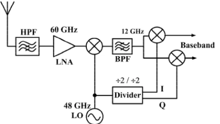
This paper presents a wide operation range 0.18Pm CMOS frequency divider for the 60GHz dual-conversion zero-IF receiver architecture as shown in Fig. 1. The dual-conversion instead of the popular direct-dual-conversion receiver architecture is chosen to relax the requirement of local oscillator and mixers. The 48GHz local oscillator (LO) used for the first stage down-conversion is feasible in the commercial 0.18Pm CMOS technology [1]. To reduce the component count and avoid mutual coupling and interference of two local oscillators on the chip, the LO for the second stage down-conversion can be obtained by dividing the 48GHz LO. In order to take advantage of the full unlicensed bandwidth at 60GHz, the operation range of the frequency divider must have wide coverage. The band switching and varactor-based frequency tuning techniques are applied for the first time to the frequency divider design to achieve wide operation range. The CMOS direct injection-locked frequency divider can
Fig. 1. Dual-conversion zero-IF receiver architecture for 60GHz radio.
operate from 43GHz to 49GHz. Operated on a 1V supply, the frequency divider consumes 8mW. To the authors’ knowledge, this work covers the widest operation range of the CMOS frequency divider above 40GHz.
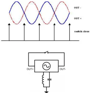
II. OPERATION OF DIRECTINJECTIONLOCK The direct injection lock technique [2] is basically the locking of the differential oscillation signals by a switch. For the LC-based implementation, the frequency divider features low power consumption and high frequency operation with respect to a fixed transistor cut-off frequency. The conceptual operation diagram is shown in Fig. 2. The differential outputs of the LC-oscillator are connected together through a switch. The LC-oscillator is free-running around half the frequency of the signal to be divided. The signal to be divided is applied to control the switch operation. As the switch closes, the differential outputs of the LC-oscillator are forced to the same voltage level. Therefore, the frequency of the oscillator is locked to exactly half the frequency of the switch-control signal.
However, the LC-based injection-locked frequency divider usually has limited locking range because the oscillator will stop oscillating far away from the LC tank resonant frequency. The locking range is inversely related to the quality factor (Q) of the resonant tank. The higher the Q, the narrower the locking range. Deliberately lowering the Q of the resonant tank to improve the locking range could deteriorate the phase noise. Raising the power consumption of the frequency divider can also
improve the locking range. Therefore, the design is traded off between power consumption, locking range, and phase noise.
III. CIRCUITDESIGN
The schematic diagram of the wide operation range direct injection-locked frequency divider is shown in Fig. 3. The cross-coupled transistor pair (M1-M2) generated the negative resistance to support oscillation. The transistor M3 works as a switch to lock down the correct frequency. The deep n-well is implemented under the switch NMOSFET such that its source and body can be tied together to avoid body effect. The body effect will increase the threshold voltage of the switch transistor and reduce the locking range. The tank inductor is a center-tapped one-turn octagonal planar inductor. The differential outputs (Ox and Oy) are connected to the
common-drain buffers for measurement purpose.
The locking range of the injection-locked frequency divider is typically much less than the full unlicensed band around 60GHz, the voltage-controlled variable PMOS capacitors are added to the resonant tanks to shift the free-running oscillation frequency. The frequency tuning with the MOS varactor is limited by Cvar/Cfix ratio,
where Cvar is the capacitance variation of the varactor and
Cfix is the fixed parasitic capacitances of varactors,
transistors, and interconnections. Adding large varactor could improve the tuning ratio, but the effectiveness is mitigated by the parasitics of transistors and interconnections. In addition, the large varactors tend to have lower Q and it will degrade the phase noise of the
Fig. 2. Conceptual operation diagram of direct injection-locked frequency divider.
Fig. 3. Schematic diagram of direct injection-locked frequency divider.
frequency divider. Therefore, the band-switching MIM capacitors are connected to the resonant tank through the transistor switches to achieve wide operation range.
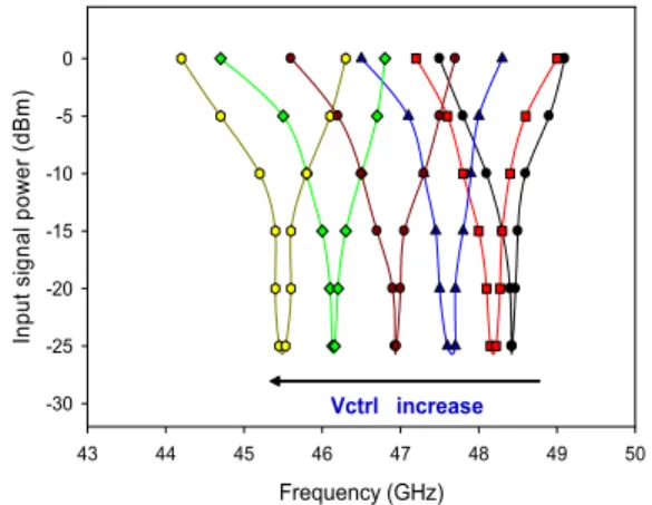
Frequency (GHz) 42 43 44 45 46 47 48 In p u t s ig nal pow er ( d Bm ) -30 -25 -20 -15 -10 -5 0 Vctrl increase
Fig. 6. Measured low-band input sensitivity of the direct injection-locked frequency divider.
Frequency (GHz) 43 44 45 46 47 48 49 50 In p u t s igna l po w e r ( d Bm ) -30 -25 -20 -15 -10 -5 0 Vctrl increase
Fig. 7. Measured high-band input sensitivity of the direct injection-locked frequency divider.
Fig. 4. Microphotograph of direct injection-locked frequency divider.
Fig. 5. Measured frequency spectrum of the frequency divider. The phase noise at 100kHz offset from 24.1GHz is -99.7 dBc/Hz.
IV. MEASUREMENTRESULT
The chip was implemented in TSMC 1P6M (1 ploy layer and six metal layers) 0.18µm CMOS technology. Fig. 4 shows the microphotograph of the direct injection-locked frequency divider. Powered by a 1V supply, the frequency divider consumes 8mW of power. The total die size is 0.54mm x 0.81mm. The core circuit area without the pads is only 200Pm x 320Pm. The measured frequency spectrum after the division is shown in Fig. 5.
Without applying the band-switching and
frequency-tuning mechanism, the measured locking range of the frequency divider is 2.6GHz. In the low band region (band-switch closed), the operation frequency covers from 43.2 to 47.3 GHz as shown in Fig. 6. In the high band region (band-switch open), the operation frequency covers from 44.2 to 49.1 GHz as shown in Fig. 7. The total operation range is from 43.2 to 49.1 GHz as the input signal power is 0dBm. When the input signal power is reduced to -10dBm, the operation range still extends from 43.8 to 48.8 GHz. The operation ranges of the low band and high band seem to have a wide overlap. It is because the parasitic capacitance is underestimated during the design and the effect of the band-switching capacitor is mitigated.
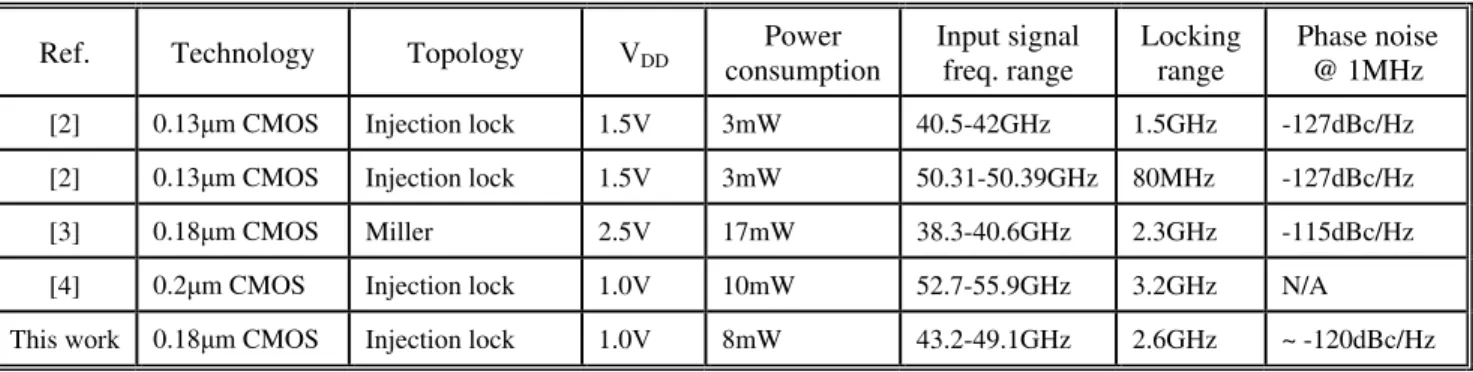
Table I. Summary of CMOS frequency divider above 40GHz.
Ref. Technology Topology VDD
Power consumption Input signal freq. range Locking range Phase noise @ 1MHz
[2] 0.13µm CMOS Injection lock 1.5V 3mW 40.5-42GHz 1.5GHz -127dBc/Hz
[2] 0.13µm CMOS Injection lock 1.5V 3mW 50.31-50.39GHz 80MHz -127dBc/Hz
[3] 0.18µm CMOS Miller 2.5V 17mW 38.3-40.6GHz 2.3GHz -115dBc/Hz
[4] 0.2µm CMOS Injection lock 1.0V 10mW 52.7-55.9GHz 3.2GHz N/A
This work 0.18µm CMOS Injection lock 1.0V 8mW 43.2-49.1GHz 2.6GHz ~ -120dBc/Hz
from the divided signal is -99.7 dBc/Hz. The phase noise at 1MHz from the divided frequency can not be properly measured because the phase noise has fallen below the noise level of the spectrum analyzer. By estimation using the trend of -20dB/decade, the phase noise at 1MHz is about -120 dBc/Hz. The measured characteristics of the frequency divider and the other published CMOS frequency dividers above 40GHz are summarized in Table I.
V. CONCLUSION
The band-switching and frequency-tuning techniques are applied to a millimeter-wave frequency divider for the first time to meet the wide operation range requirement of the emerging 60GHz application. Implemented in the 0.18Pm CMOS technology, the direct injection-locked frequency divider can cover the operation frequency from 43.2 to 49.1GHz. The measured phase noise is -99.7 dBc/Hz at 100kHz offset and roughly -120 dBc/Hz at 1MHz from the signal after division. Operated at 1V, the frequency divider consumes 8mW. The core area of the frequency divider occupies 200Pm x 320Pm of the silicon estate. This work demonstrates the validity of band-switching and frequency-tuning techniques for extending the operation ranges of frequency dividers. To the
authors’ knowledge, this work achieves the widest operation range of the millimeter-wave CMOS frequency divider above 40GHz.
ACKNOWLEDGEMENT
The authors wish to acknowledge the assistance and support of National Science Council, National Chip Implementation, and NTU-MediaTek Wireless Research Laboratory.
REFERENCES
[1] T.-N. Luo, S.-Y. Bai, Y.-J. E. Chen, H.-S. Chen, and D. Heo, “A 1-V CMOS VCO For 60-GHz Applications,” in
Proc. IEEE Asia-Pacific Microwave Conference, December
2005, pp. 370-373.
[2] Marc Tiebout, “A CMOS Direct Injection-Locked Oscillator Topology as High-Frequency Low-Power Frequency Divider,” IEEE Journal of Solid-state Circuits, vol. 39, no. 7, pp. 1170-1174, July 2004.
[3] Jri Lee and Behzad Razavi, “A 40-Ghz Frequency divider in 0.18-µm CMOS Technology,” in IEEE Symp. VLSI
Circuits Dig. Tech. Papers, June 2003, pp. 259-262.
[4] Ken Yamamoto and Minoru Fujishima, “55GHz CMOS Frequency Divider with 3.2GHz Locking Range,” in Proc.
30th European Solid-State Circuits Conference ESSCIRC