國
立
交
通
大
學
電子工程學系電子研究所碩士班
碩
士
論
文
解決工程改變中所產生之輸入扭轉違規與輸出負
載違規
A Metal-Only-ECO Solver for Input-Slew and Output-Loading
Violations
研 究 生:張智為
指導教授:趙家佐 博士
A Metal-Only-ECO Solver for Input-Slew and Output-Loading
Violations
研 究 生:張智為 Student:Chih-Wei Chang
指導教授:趙家佐 Advisor:Chia-Tso Chao
國 立 交 通 大 學
電子工程學系電子研究所碩士班
碩 士 論 文
A ThesisSubmitted to Department of Electronics Engineering & Institute of Electronics College of Electrical and Computer Engineering
National Chiao Tung University in partial Fulfillment of the Requirements
for the Degree of Master
in
Electronics Engineering January 2010
Hsinchu, Taiwan, Republic of China
i
解決工程改變中所產生之輸入扭轉違規與輸出負
載違規
學生:張智為 指導教授:趙家佐 博士
國立交通大學電子工程學系電子研究碩士班
摘
要
為了縮短電子產品上市時間及減少在先進製程光罩上的巨額花費,繞線工
程改變已成為具吸引力與實際的解決方案。在使用繞線工程改變時,由於
電路上有限的備份電路單元造成新加入的電路常會造成時序上的輸入扭轉
違規與輸出負載違規使得電路時序上出錯。這篇論文提出一個解決輸入扭
轉違規與輸出負載違規的架構,藉由連接備份電路單元作為緩沖電路以解
決新產生之電路延遲問題。我們提出兩種插入緩沖電路方法依序最小化所
使用的緩沖電路及解決時序上有所違背的電路節點。這樣的架構已經在業
界所使用的電路上驗證過。實驗數據表明我們所提出的架構相對於商業軟
體可以使用更少的緩沖電路、更少的中央處理器運行時間去解決更多時序
上延遲問題。整個架構建築在現有的自動繞線及擺放工具上並且可以方便
的應用到不同的工具中。
ii
A Metal-Only-ECO Solver for Input-Slew and Output-Loading Violations
Student: Chih-Wei Chang Advisor: Dr. Chia-Tso Chao
Department of Electronics Engineering
Institute of Electronics
National Chiao Tung University
Abstract
To shorten the time-to-market and reduce the expensive cost of photomasks in
advance process technologies, metal-only ECO has become a practical and
attractive solution to handle incremental design changes. Due to limited spare
cells in metal-only ECO, the new added netlist may often violate the input-slew
and output-loading constraints and, in turn, delay or even fail the timing closure.
This paper proposes a framework, named MOESS, to solve the input-slew and
output-loading violations by connecting spare cells onto the violated nets as
buffers. MOESS provides two buffer insertion schemes performed sequentially
to minimize the number of inserted buffers and then to solve timing violations if
there is any. This framework has been silicon-validated through industrial
designs with more than 1-million instances. The experimental results
iii
and less CPU runtime compared to an EDA vendor’s solution. The whole
framework is built based on a commercial APR tool and can be ported to any
other APR tool offering open access to its design database.
iv
誌
謝
在新竹這幾年的生活就要畫上句點,所有的歡笑、挫折、沮喪、興奮也已
成為過去。很感謝爸媽一直陪伴著在身邊,困惑時指點方向、難過時給予
力量、高興時一同分享;也很感謝恩師 趙家佐教授不僅提供學術上的建
議讓我對測試領域有所了解,並且在生活上分享經驗讓我能有所成長;另
外實驗室的學長、同學、學弟們所給予的支持,包括育澤、啟銘、偉盛、
弘晰、皓宇、思邦、淳仁、擴安、遵銘,在學術上有所疑問時互相討論,
在生活中互相分享彼此的看法;還有我的大學同學們,煌仁、家縉、達
生、大叔、盛元等,討論彼此的人生規劃,讓我對未來有所期待。最後,
再次向所有曾經關心、支持、幫助過我的人獻上祝福,沒有你們的支持就
沒有現在的我。
2010 年 張智為 撰於新竹
v
Contents
摘要 ………..……… i Abstract ……….. ii 誌謝 ……… iii Contents ……….… iv List of Tables ……….…. v List of Figures ………. vi 一〃 Introduction ………..……… 1 二〃 PRELIMINARIES .……….…….... 5三〃 OVERVIEW OF PROPOSED METAL-ONLY ECO SLEW/LOADING SOLVER …..……….. 8
四〃 ESB AND ECT BUFFER-INSERTION SCHEMES ………...… 13
五〃 EXPERIMENT RESULT ………...… 24
六〃 CONCLUSION ………... 28
vi
List of Tables
Table I Comparison between MOESS and [3] on solving slew, loading, and timing violations for multiple metal-only ECO projects ………..…… 27 Table II Comparison between MOESS and [3] on solving slew, loading, and timing violations
vii
List of Figures
Figure 1 Flow and an example of converting a slew constraint to a loading constraint ... 6
Figure 2 Overall flow of MOESS ………... 8
Figure 3 ExamPle of converting functional gates to buffers …………..……..………. 10
Figure 4 Example of inserted buffers for different pin grouping ………. 14
Figure 5 Flow of ESB buffer-insertion scheme ………. 15
Figure 6 Minimum Chain algorithm ……… 16
Figure 7 Search buffer in the ORL diamond shape ……… 19
Figure 8 MC buffer insertion algorithm ………... 21
Figure 9 An example process of ESB buffer-insertion scheme ………. 22
Figure 10 Spare buffers in the intersection before (a) and after (b) backward tolerance ………..……….. 22
Figure 11 (a) spare empty area(placement/routing obstacle) (b) spare gate search failed (c) detour insertion ………. 23
1
I. INTRODUCTION
The increasing pressure of time-to-market has forced the IC design houses to improve its capability of handling incremental design changes, such as ECO (engineering change order), instead of starting another design respin. Those incremental changes may result from the specification revision requested from the system integrators, who might catch a system-design error after first integration or attempt to slightly enhance the original functions. Also, some incremental changes are requested by the IC design house to fix design errors captured in silicon debugging or eliminate systematic defects for yield improvement. All the above changes occur after the first silicon chips are produced, implying that the original photomasks have to be replaced for the design changes.
In current process technologies, the cost of photomasks increases by an order of
magnitude per generation [1][2]. For sub-100 nm technologies, the cost of a full photomask set could reach 1 million USD [1][2]. To reduce this expensive cost of photomasks, the above incremental design changes are enforced to be implemented by changing only the metal layers while the base layers (for cells) remain the same. As a result, the original photomasks used for printing the cells can be reused in the next tape-out. This reuse of the base-layer photomasks can not only save the cost of photomasks themselves but also reduce the tape-out turn-around time since the base layers could be manufactured in advance. This type of the incremental design changes is referred to as the metal-only ECO.
2
To realize metal-only ECO and make it more effective, some new design techniques have to be developed. First, spare cells need to be spread all over the design so that the change can be implemented in every possible location. This allocation of spare cells directly determines the affordable ECO size and its area overhead. EDA vendors already provide some solutions to it [3][4][5]. Second, a more complicated router is required to efficiently handle a large
number of existing obstacles and design rules in ECO. Some previous work addressed these issues by using an implicit connection graph [6], a graph-reduction technique [7], or a timing-aware router [8]. Third, the violations of timing factors may significantly increase after metal-only ECO. Thus, a solver which can automatically remove those timing-related violations is needed to shorten the timing closure of metal-only ECO. Unfortunately, the current solutions provided by EDA vendors are not effective so far.
Input slew and output loading are two important timing factors to sign off the timing closure, which are limited by the slew constraint and loading constraint, respectively. Any violation to these two constraints may lead to a wrong timing estimation of the design, and in turn, degrade its performance and yield. In reality, meeting the slew constraint is even more crucial than meeting the timing constraint (more specific, setup-time constraint). In most cases when the slew constraint is met, its timing constraint can also be met [9][10]. Several buffer-insertion techniques [9][10][11][12][13] are proposed to solve the violation of the slew, loading, and timing constraint. However, most previous works assume that its gate placement is able to change, and hence cannot be applied to metal-only ECO.
3
In metal-only ECO, solving the timing-related violation relies on the utilization of pre-placed spare gates. [14] proposed a technology-remapping technique to fix timing violations, which may require more pre-placed spare cells to support the desired remapping. [15] inserted constant values to the inputs of spare cells and applied a technology-mapping technique to replace the original cells with spare cells. It may require more universal but larger-area spare cells, such as AOI and MUX. Some commercial tools also provide options to support buffer insertions in metal-only ECO. However, the final location of the inserted buffers often deviates from the ideal location due to the lack of physical information on spare cells and routing resources during the buffer insertion.
In this paper, we develop a metal-only-ECO framework, named MOESS (Metal-Only Eco Slew/cap Solver), to solve slew and loading violations by using pre-placed spare gates as inserted buffers. This framework also can solve the timing violations, implicitly or explicitly. For each violation, the proposed framework first finds the best buffer candidates from all spare gates and utilizes a commercial back-end tool to insert the selected buffer through its interface. Therefore, the focus of this framework is not on building a complete ECO router to handle obstacles and constraints, but on accurately estimating the input slew and output loading of the buffers newly inserted with the adopted back-end tool. This framework can be applied based on any commercial back-end tool as long as the design database can be
queried through an open interface, such as Milkyway for Synopsys, OpenAccess for Cadence, or Volcano for Magma.
4
In addition, two buffer-insertion schemes are provided in the proposed framework
sequentially. The first scheme applies the minimum-chain algorithm to minimize the number of spare gates in use, followed by the second scheme to solve timing violations created by the first scheme, if there is any. The framework has been silicon-validated through industrial designs with more than 1-million instances. The experimental results show that, compared to an EDA vendor’s solution, the proposed framework can solve more slew and loading
violations with less spare gates and less CPU runtime. This framework is currently applied in industry.
5
II. PRELIMINARIES
A. Current Metal-Only ECO Flow
Most current APR tools apply the following two steps to realize metal-only ECO: netlist difference followed by spare cell mapping. In the netlist-difference step, tools first identify the new added cells by comparing the new netlist to be ECO with the original netlist. The added cells are assumed to be placed in an ideal area, which may not be valid. In the spare-gate-mapping step, the tools map the new added cells to physical spare cells. However, when the ECO size is large, those spare cells may not always be found in the ideal area and tools need to search for the nearby gates to substitute. Thus, violations of slew, loading, and setup-time constraints may occur here.
To eliminating these violations, APR tools use a similar approach, inserting buffers in the netlist and mapping buffers into spare gates. However, the spare buffers may not be found in the desired area. Hence the violations remain unsolved or even become worse since the wire loading of the new-added interconnect may exceed the constraint as well. This unexpected violation can be attributed to the insufficient number of available spare buffers and the lack of physical information on the spare buffers during the mapping step.
B. Transfer Slew Constraint into Loading Constraint
The output slew of a gate is determined by its input slew and its output loading. An
excessive output loading at the current gate will result in an excessive input slew at its fanout gates. Therefore, to control the output loading of its fanin gates can avoid the input-slew
6
violation of the current gate. In other words, we can transfer the problem of solving input-slew violations for the current pin into the problem of solving output-loading violation for its fanin gates.
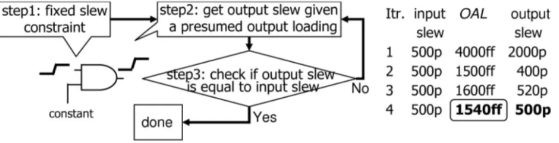
We first define the output available load of a gate g, OALg , as the maximum output loading
of g which can generate a output slew smaller than the slew constraint assuming that the input slew of g is equal to the slew constraint. Through table look-up of the timing library and
interpolation, this OALg can be obtained after a binary search of the output slews
corresponding to different output loadings. Figure 1 illustrates the detailed steps of obtaining
this OALg . In step 1, input slew of gate g is set to the maximum allowed slew. In step 2, the
output slew associated with a presumed OALg is obtained by table look-up. In step3, we check
if the output slew is the same as the slew constraint. If yes, then stop searching. Otherwise, if the output slew is larger than the slew constraint, we presume a lower output loading and repeat step 2. If the output slew is less than the slew constraint, we presume a higher output loading and repeat step 2.
Fig. 1. Flow and an example of converting a slew constraint to a loading constraint.
In most cases, the obtained OALg associated with the slew constraint is smaller than the
7
loading constraint. However, for some gates with weak driving capability, the OALg associated
with the slew constraint may exceed the loading constraint. In this case, we set OALg to the
8
III. OVERVIEW OF PROPOSED METAL-ONLY ECO
SLEW/LOADING SOLVER
A. Overall Flow of MOESS
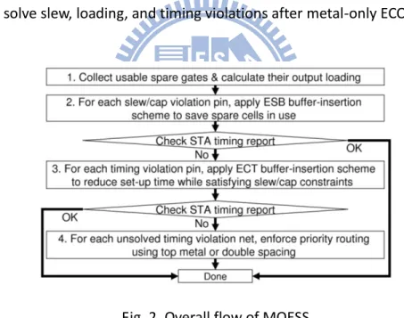
After the metal-only ECO is finished by using netlist difference and spare cell mapping (Section II-A), tools will report the pins violating slew and loading constraints. From this violation report, MOESS will automatically generate the corresponding command script of a commercial APR tool to solve the violations. Figure 2 shows the overall flow of MOESS, which is designed to solve slew, loading, and timing violations after metal-only ECO.
Fig. 2. Overall flow of MOESS
The first stage of MOESS is to increase the candidate pool of spare buffers by collecting usable spare cells. Section III-B describes the details. The second stage of MOESS is to apply ESB (Eco Save Buffer) buffer-insertion scheme to solve the slew and capacitance violations using minimum buffers. A minimum-chain algorithm is used in the ESB scheme to guide the order inserted buffers. After the slew violations are solved, most timing violations can be
9
solved as well. Then a timing analysis tool will report the remaining critical paths violating timing constraint. Along those critical paths, we identify the nets which are inserted with buffers in stage 2. Then, we perform the ECT (Eco Care Timing) buffer-insertion scheme to re-insert buffers and shorten setup time while solving slew and loading violations. The details of ESB and ECT buffer-insertion schemes are provided in Section IV. For the timing violations which cannot be solved by solving the slew violation, MOESS will perform its last stage to enforce the priority routing of the critical nets by using top metal (reducing resistance) or double spacing (reducing coupled capacitance), and re-route the other non-critical nets accordingly. These two options (top mental and double space) are provided by most of current commercial APR tools.
B. Enlarge Candidate Pool of Spare Buffers
Current commercial APR tools use only the spare gate labeled as”buffer-type” to perform buffer insertion. More aggressively, MOESS exploits the pool of spare buffers by recycling the redundant cells and using functional spare gates as buffers.
1. Recycle of Redundant Cells: During implementation stage, most APR tools use a special tag to recognize spare gates. However, the tag could be lost when designers or APR engineers incorrectly operate. In MOESS, we recycle those lost-tag gates as spare gates. In addition, designer sometimes might remove certain functionality of a module. Thus, MOESS applies a breadth-first-search algorithm to recycle the redundant gates starting from each floating output.
10
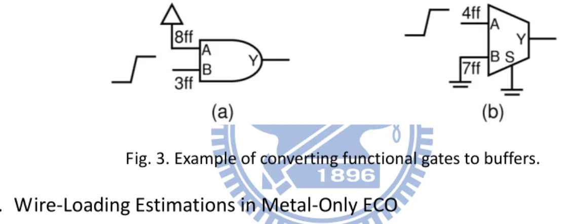
2. Use Functional Cells as Buffers: In MOESS, spare functional cells can also be used as buffers by connecting Vdd or Gnd to cells’ side inputs. The cell’s input used as buffer’s input is the pin with least capacitance. For example in Figure 3(a), an AND gate contains two inputs with 8ff and 3ff input capacitance each. To convert this AND gate to a buffer, the input pin with larger capacitance is connected to the non-controlling value, Vdd. The input pin with smaller capacitance is used as the buffer input. These connection choices can speed up the gate propagation delay by avoiding the charge of high-capacitance input. A similar concept can be applied to convert a MUX to a buffer (Figure 3(b)).
Fig. 3. Example of converting functional gates to buffers.
C. Wire-Loading Estimations in Metal-Only ECO
Another barrier to effective the buffer insertion in metal-only ECO is the estimation to the wire loading of a new interconnect. The wire length of a new interconnect varies from
different levels of routing congestion, and cannot be simply measured by Manhattan distance. A more accurate estimation to the wire loading can be obtained by doing the routing first and then extract its RC, which is time-consuming and not applicable when building an efficient buffer-insertion scheme. Therefore, to solve the slew and loading violation with minimum buffers, our metal-only-ECO framework needs to not only enlarges the candidate pool of spare cells but also efficiently estimates the wire loading considering the level of routing congestion.
11
The wire loading is linearly proportional to the wire length. If all routing resources can be used, the wire length will follow the Manhattan distance. However, with existing
interconnects, the wire length may be larger than the Manhattan distance depending on the level of routing congestion. In MOESS, we use the via density, denoted as VD(p1, p2), to represent the routing-congestion level in a rectangular area between two connected pins p1 and p2. VD(p1, p2) = VA/area, where VA is the area of the occupied vias and area is the rectangular area formed by using p1 and p2 as its two diagonal vertices.
Then, we define the routing ratio to Manhattan distance, denoted as RRMDh(vd)
(RRMDv(vd)), to represent the ratio of the actual wire length over the Manhattan distance
between connected pins in horizontal (vertical) direction. This ratio is a function of the via
density vd. In MOESS, this RRMDh(vd) or RRMDh(vd) is obtained by the average statistical
result accumulated in the past usage of the adopted APR tool. This statistical result varies according to different APR tools in use. Based on this ratio, we can use the following equation to compute the wire loading corresponding to a horizontal (vertical) unit of the Manhattan
distance between two pins p1 and p2, denoted as Uh(p1, p2) (Uv (p1, p2)):
Uh(p1, p2) = RRMDh(VD(p1, p2)).Kh (1)
Uv(p1, p2) = RRMDv(VD(p1, p2)).Kv (2)
where Kh (Kv) represents the wire loading per unit in the horizontal (vertical) direction
according to the process technology. Last, the wire load between two pins p1 and p2,
12
WL(p1, p2) = MDh(p1, p2).Uh(p1, p2) + MDv(p1, p2).Uv(p1, p2) (3)
where MDh(p1, p2) (MDv (p1, p2)) represents the Manhattan distance in horizontal (vertical)
13
IV. ESB AND ECT BUFFER-INSERTION SCHEMES
For an input-slew-violation pin p, we first calculate its equivalent OALg by the method
described in Section II-B, where g’s output directly connects to p. Then the slew-violation problem at input pin p is transferred to an equivalent loading-violation problem at
gate g’s output. The gate g is referred to the violation gate and the net driven by g is referred to the violation net. We first apply the ESB buffer-insertion scheme to minimize the number of spare cells used to solve this loading-violation problem. The more spare cells can be saved, the larger ECO size can be implemented in the next generation of ECO. From our experience, a product could have more than 10 generations of ECO due to either large market requests or poor design.
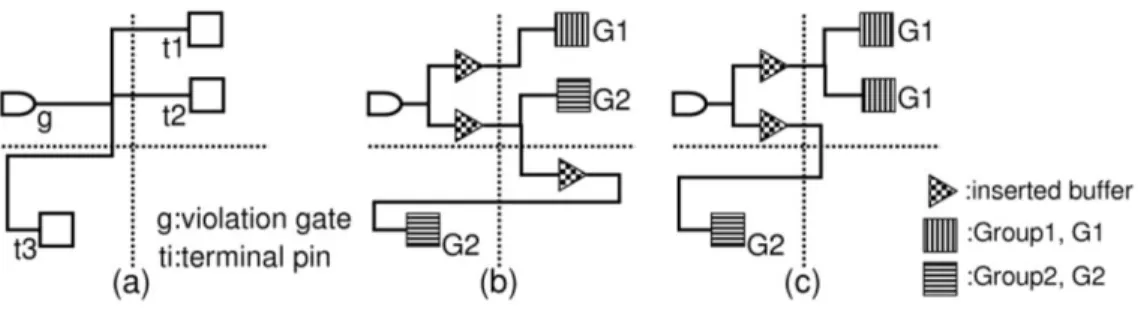
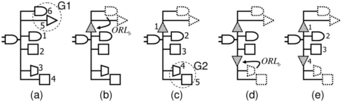
In reality, most slew violations result from high-fanout nets. To save the spare buffers in use, we try to use one buffer to drive as many terminal pins as possible. Therefore, we need an effective grouping method to select the nearby terminal pins which can be driven by a common buffer under the loading or slew-transferred constraint. Figure 4 shows an example of a 3-terminal violation net. If we group two geometrically separated pins, such as t2 and t3 in Figure 4(b), one buffer is not enough to drive both of t2 and t3 since their wire loading is too large. However, if we group two nearby pins, such as t1 and t2 in Figure 4(c), one buffer is enough to drive both of t1 and t2.
14
Fig. 4. Example of inserted buffers for different pin grouping.
Figure 5 shows the flow of the ESB scheme. In step A, a minimum-chain algorithm is applied to obtain an order of terminal pins for the violation net, named MC order (detailed in Section IV-B). This MC order can guide the grouping of nearby terminal pins in step B
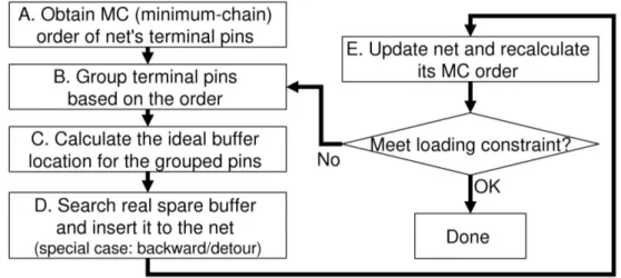
(detailed in Section IV-B). Step C calculates the ideal location of the inserted buffer based on the grouped terminal pins (detailed in Section IV-C). In step D, we attempt to map a real spare buffer closest to the ideal location while satisfying the slew-transferred loading constraint (detailed in Section IV-D). After a real spare buffer is successfully inserted, we update the violation net and recalculate the MC order of its terminal pins in step E. We repeat step B to step E until the output loading of the violation gate meets the slew-transferred loading constraint. An overall algorithm is provided in Section IV-E. We also discuss how to relax the searching criteria when no suitable buffer c an be found to solve the violation in Section IV-F. Section IV-G describes how to handle hard macros in the ESB scheme.
15
Fig. 5. Flow of ESB buffer-insertion scheme.
The ECT buffer-insertion scheme is applied after ESB scheme. The objective of ECT scheme is to eliminate the timing violations resulted from using ESB scheme. The flow of ECT is similar to the ESB scheme except the grouping method in step B. The details are described in Section IV-H.
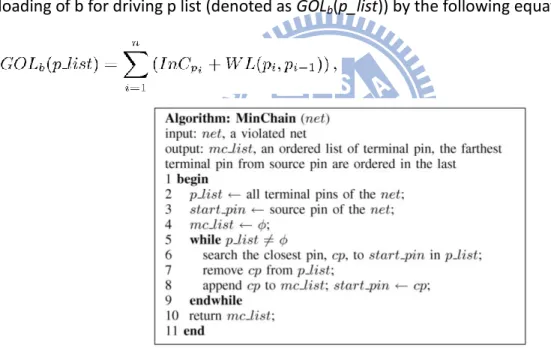
A. Obtain Minimum-Chain Order of Terminal Pins
As the example in Figure 4 shows, we hope to group the terminal pins of the violation net not only in the same geometrical neighborhood but also in the same direction toward the violation gate. Otherwise the wire loading to drive the grouped pins may be too large. In order to obtain such grouping, we modified a minimum-chain algorithm in [16] to get the MC order of terminal pins. The concept of this minimum-chain algorithm is to assign the closest pin as the next ordered pin each time, starting from the violation gate g (the order of g is 0). By connecting the terminal pins one by one with such order, their total wire length can approach to minimal. This property also implies that the terminal pins with adjacent MC order are more likely in the same direction toward the violation gates as well. Figure 6 lists
16
this minimum-chain algorithm.
B. Group Terminal Pins Using MC Order
In step B, terminal pins of the violation net are first grouped assuming a type-t buffer b is used. We start from the buffer type with the highest driving capability to the one with the lowest. Then, we follow the MC order to serially add the terminal pins into the group p list. The objective here is to obtain a group of pins p list such that the output loading of b for
driving all grouped pins in p list is close to but not exceed the OALb. We estimate this output
loading of b for driving p list (denoted as GOLb(p_list)) by the following equation:
(4)
Fig. 6. Minimum Chain algorithm
where n is the size of p list, pi is the ith ordered pin in p list, InCpi is the input capacitance of pi,
WL(pi, pi−1) is defined in Equation 3, and WL(p1, p0) is equal to 0.
In this estimation, we assume that the terminal pins are piece-wise connected one by one. However, the real routing of a net generated by commercial tools is like a Steiner tree, where
17
multiple terminal pins may share one common wire. Therefore, this estimation is actually an upper bound, implying that the inserted buffer by ESB scheme can safely meet the loading constraint.
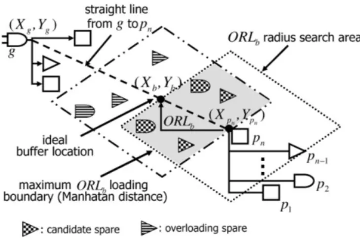
C. Calculate Ideal Buffer Location
We follow the following two rules when deciding the ideal location of the type-t buffer to drive all terminal pins in p list:
R1 Use all buffer’s driving capability under the given constraint.
R2 Locate the inserted buffer as close to the violation output as possible.
To achieve R1, we first calculate the output remained load of the buffer b, denoted as ORLb,
using the equation:
(5)
The amount of ORLb determines the affordable wire length connecting from inserted buffer b
to the last-ordered pin pn in p_list. The higher ORLb, the longer wire length can be allowed
between b and pn. Thus, the ideal location of the inserted buffer b must satisfy the following
equation:
(6)
where Xa and Ya represents the X-axis and Y-axis coordinates of pin (or gate) a, respectively. To
make the buffer b closer to the source pin g, we limit the ideal location of b on the straight
line between g and pn. Then we add another equation:
18
Last, we can obtain the ideal location of b by solving both Equations 6 and 7, assuming the equality holds in Equations 6.
D. Search Real Spare Gate
We first use the Manhattan distance between the last-ordered pin pn and the ideal buffer
location as the radius to draw a diamond-shape region centered at pn. The buffer found in this
diamond-shape region can satisfy Equations 6. To make the buffer closer to the violation gate g, we use the same radius to draw another diamond-shape region centered at the ideal buffer location. We then attempt to select the buffers locating in the intersection of the two regions. This searching can make sure that the selected buffer, if any, is on the way toward the
violation gate g, which helps to achieve R2. Figure 7 shows an example of these two diamond-shape regions.
Finally, we select the type-t buffer closest to the ideal location in the intersection region. If such type buffer cannot be found in the intersection region, then we change the buffer type to one with lower driving capability and repeat step B to step D.
19
Fig. 7. Search buffer in the ORL diamond shape
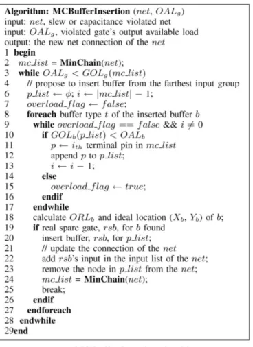
E. Overall Algorithm of ESB Scheme
Figure 8 details the general algorithm of ESB scheme. In this algorithm, Line 6 to 17
corresponds to step B in Section IV-B. Line 18 corresponds to step C in Section IV-C. Line 19 to 20 corresponds to step D in Section IV-D.
Figure 9 illustrates the process of inserting buffers onto a 6-terminal violation net. In Figure 9(a), the labeled number on each terminal represents its MC order. We first group the
farthest pins in G1 (5 and 6) according to step B. In Figure 9(b) a spare buffer is inserted to share the loading of grouped pins through step C and D. Pin 5 and 6 are hence removed from
the violation net. Assume OALg is still less than GOLg (mc list) in this case, we need to
recalculate the MC order for the updated violation net with 5 terminal pins. Then we repeat the step B, C, and D to group terminal pins in Figure 9(c) and insert another buffer for the
grouped pins in Figure 9(d). After that, OALg become less than GOLg (mc list). So total two
20
F. Background Tolerance
In order to drive as many terminal pins as possible, we keep on adding terminal pins into the grouping list p list as long as GOLb(p_list) is less than OALb. A larger GOLb(p_list) will result
in a smaller ORLb (as defined in Equation 5) and, in turn, a smaller radius of the two
diamond-shape regions. This radius reduction may shrink the searching space of candidate spare buffers, such as the situation in Figure 10(a). Therefore, when no candidate spare buffer can be found to drive the pins in p list, we may remove the last-ordered pin in p list to increase
ORLb. Then we restart the searching for candidate spare buffers, such as the situation in
Figure 10(b).
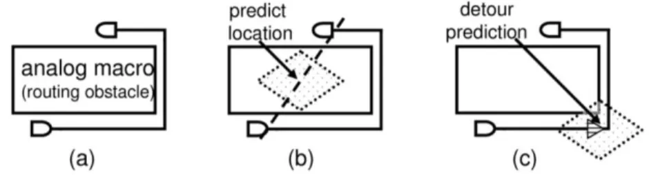
G. Detour Insertion to Avoid Hand Macro
In seldom cases, the violation net contains terminal pins locating on the opposite two sides of a hard macro such as Figure 11(a). The predicted location of the inserted buffer may be inside the hard macro such as Figure 11(b). To avoid this situation, MOESS need record the area of hard macros in advance. Once the predicted buffer region is located in hard macro’s area, we perform a detour search along the boundary of the hard macro to find a proper buffer such as Figure 11(c). In such a case, the search could be from either direction of the source pin. In MOESS, we start from the direction which can form a shorter detour path to the target pin.
H. ECT Buffer-Insertion Scheme
21
Although the slew or loading violation can be solved by ESB scheme, the delay of some paths may exceed the timing constraint due to the extra gate delay of inserted buffers. This case usually occurs when a new-added function is connected to a timing-critical net. After studying those timing-violation cases, we found that most violations result from the sharing of a
common buffer between a timing-critical path and long new-added wires, such as the case in Figure 12(a). The labeled number for each pin represents its Manhattan distance to the source pin of the violation net. Those new-added wires can be designed as multi-cycle paths to meet the timing constraint but the original paths cannot.
22
Fig. 9. An example process of ESB buffer-insertion scheme.
To avoid such cases, ECT buffer-insertion scheme will separate the grouping of long-wire terminal pins from the others. So the terminal pins on critical paths need not to share a
common buffer with other long-wire terminal pins, such as the case in Figure 12(b). Therefore, ECT scheme basically follows the same flow of ESB scheme but change the step of terminal-pin grouterminal-ping (step B). In ECT scheme, a terminal terminal-pin whose Manhattan distance to the source pin exceeds a threshold is defined as the wire terminal pins. Then, for only those long-wire terminal pins, we determine the pin grouping using the same procedure described in Section IV-B and insert buffers accordingly. After that, the same procedure is applied to the other terminal pins again. As a result, the number of inserted buffer may be increased while the propagation delay for critical paths can be reduced.
23
Fig. 11. (a) spare empty area(placement/routing obstacle) (b) spare gate search failed (c) detour insertion
The threshold of the Manhattan distance to the source pin is actually a parameter in ECT scheme. ECT scheme will try different thresholds within an empirical range to check if the timing violation can be solved. If not, ECT scheme will report the case with the best negative slack.
24
V. EXPERIMENTAL RESULT
Our platform is Linux, kernel 2.6.9-11.elsmp, running on AMD Opteron processor 250 with 16GB memory. The ECO flow, including netlist difference, spare gate mapping, and routing, is performed based on a commercial APR platform [3]. After the metal-only ECO is performed, we first obtain the violation report on slew, loading, and timing constraints. Then MOESS will generate corresponding scripts based on this violation report to insert and map spare buffers onto violation nets. We compare the results of MOESS with a EDA vendor’s buffer-insertion solution for metal-only ECO [3]. In vendor’s solution, we use the command”run gate buffer wire -slew/cap -eco” to insert buffers for each violation net.
The benchmarks used in this experiment are all industrial projects. The spare-cell count in each project is 3% to 5% of the total cell count. The spare cells are evenly placed within the chip by using an in-house tool before the base-layer tape-out. The slew constraint in use is a pre-defined constant associated with the process technology and the cell library. The loading constraint in use is defined as a ratio to the value of the library-suggested constraint. In our experiments, the slew and loading constraints are 2.2ns and the ratio of 1 for the .18um process; the slew and loading constraints are 1.0ns and the ratio of 1.2 for the .13um process.
25
Fig. 12. Buffer insertion in a critical path by (a) ESB scheme and (b) scheme.
In the Table I, we first report the comparison results on 7 industrial projects. Column 1 lists the project name and its ECO version in parentheses. Columns 2 to 5 list the instance count, the adopted process technology, the spare-cell count, and the size of ECO in instances for each project, respectively. Columns 6 and 7 list the numbers of reported slew violations and loading violations, respectively, before any buffer-insertion scheme is applied. Column 8-10, 12-14, and 16-19 list the worst input slew, the worse output-loading ratio to the library-suggested constraint, and the worst slack, respectively, reported (1) before any buffer-insertion scheme is applied (denoted by ori.), (2) after a EDA vendor’s solution is applied (denoted by [3]), and (3) after MOESS is applied (denoted by MOESS). Column 11, 15, and 19 also list the improvement of MOESS over [3] (denoted by imp.) in the worst input slew, the worse output-loading ratio, and the worst slack, respectively. The number followed by a ”*” means that the corresponding value violates the constraint. In Column 20-22 and 23-25, we report the number of spare buffers in use and the CPU runtime for both [3] and MOESS, and the corresponding improvement or speedup of MOESS over [3].
As the results show, MOESS can solve all the slew, loading, and setup-time violations for these seven projects while the vendor’s solution violates the slew constraint in 3 projects, the
26
loading constraint in 2 projects, and the setup time constraint in 4 projects. The average improvements of MOESS on the worst slew, worst loading, and worst slack are 24%, 21%, and 57%. Also, the number of used spare buffers by MOESS is smaller than that by [3] for each project, which saves more ECO resources for the next generation of ECO. This reduction to the number of used spare buffers is 38% in average. Furthermore, the runtime consumed by MOESS is less than that by [3] for each project as well. The average speedup of MOESS is 14.9X. One key reason why MOESS is faster than [3] is that MOESS utilizes the MC-ordering-based method to quickly estimate the wire loading and group terminal pins (Section IV-B). The commercial tool [3] needs to construct a Steiner-tree-like net-routing before estimating its loading, which requires more computation time. These experimental results demonstrate both the effectiveness and efficiency of our buffer-insertion algorithm.
To show a stronger need of an effective metal-only-ECO solver when the ECO resource is limited, we report the experimental results of different ECO generations on a single project in Table II. In the 2nd and 3rd ECO generations, the size of new added functions
is small and hence both MOESS and [3] solve all the violations. However, after a large scale ECO is requested in the 5th ECO generation, [3] fails to solve the slew, loading, and timing violation while MOESS can solve all of them with less spare buffers and less runtime. Note that the number of remaining spare gates is only 0.5% to the total number of instance after the 5th ECO generation. Therefore, even though ECO size is small in the 7th and 8th ECO generation, [3] still fails to solve the slew and setup-time violations. On the contrary, MOESS solves all the slew and loading violations and controls the slack at an acceptable level, -0.1ns,
27
for both ECO generations. Actually we taped out these two ECO generations with this slack of -0.1ns because this negative slack cannot be removed with further manual effort. The slacks resulted from [3] in these two ECO generations are -1.7ns and -0.5ns, respectively, which is far away from the tape-out standard and requires a lot manual effort to achieve the timing closure. This experimental result again demonstrates the strength of MOESS in metal-only ECO.
Table I
Comparison between MOESS and [3] on solving slew, loading and timing violations for multiple metal-only ECO projects.
Table II
Comparison between MOESS and [3] on solving slew, loading, and timing violations for different ECO generations of a single project.
28
VI. CONCLUSION
In this paper, an efficient and effective framework is proposed to solve the slew, loading, and timing constraint in metal-only ECO. The proposed framework is built based on the platform of a commercial APR tool. It can also be ported to any other commercial tool offering open access to the design database. According to the experimental results obtained from real industrial projects, the proposed framework can significantly increase affordable scale of mental-only ECO with less spare gates and runtime in use, compared to a current vendor’s solution. This framework is currently included in the ECO flow of an IC design house.
29
REFERENCES
[1] International technology roadmap for semiconductors http://www.itrs.net/ [2] A. Balasinski, Optimization of sub-100-nm designs for mask cost reduction, J.
Microlithography, Microfabrication, Microsyst., vol.3, pp.322-331, Apr. 2004. [3] Magma Design Automation, http://www.magma-da.com/
[4] Synopsys Inc., http://www.synopsys.com/
[5] Cadence Design System, http://www.cadence.com/
[6] J. Cong, J. Fang, and K. Khoo, An implicit connection graph maze routing algorithm for ECO routing, ACM/IEEE Int’l Conference on Computer Aided Design, pp.163-167, Nov., 1999.
[7] Yih-Lang Li, Jin-Yih Li, and Wen-Bin Chen, An efficient tile-based ECO router using routing graph reduction and enhanced global routing flow, IEEE Trans. on Computer-Aided Design of Integrated Circuits and Systems, Vol. 26, No. 2, pp.345-358, Feb., 2007.
[8] S. Dutt, and H. Arslan, Efficient timing-driven incremental routing for VLSI ciruits using DFS and localized slack-satisfaction computations, Design, Automation, and Test in Europe, Vol. 1, pp.768-773, 2006
[9] Weiping shi and Zhuo Li, Fast algorithm for optimal buffer insertion, IEEE Trans. on CAD, pp.492-498, 2005.
[10] P.J. Osler, Placement driven synthesis case studies on two sets of two chips: hierarchical and flat, ACM Int’l Symposium on Physical Design, pp. 190-197, 2004.
Minimum-30
buffered routing of non-critical nets for slew rate and reliability control, ACM/IEEE Int’l Conference on Computer Aided Design, pp.408-415, 2001.
[12] P. Saxena and N. Menezes and P. Cocchini an D.A. Kirk-patrick, Repeater scaling and its impact on CAD, IEEE Trans. on Computer-Aided Design of Integrated Circuits and Systems, vol. 23, no. 4, pp. 451-463, 2004.
[13] S. Hu, C.J. Alpert, J. Hu, S.K. Karandikar, Z. Li, W. Shi, and C. Sze, Fast algorithm for slew-constrained minimum cost buffering, Design Automation Conference, pp. 308-313, 2006. [14] Y.P. Chen, J.W. Fang and Y.W. Chang, ECO timing optimization using spare cells and
technology remapping, ACM/IEEE Int’l Conference on Computer Aided Design, pp.530-535, Nov., 2007.
[15] Y.M. Kuo, Y.T. Chang, S.C. Chang and M. Marek-Sadowska, Engineering change using spare cells with constant insertion, ACM/IEEE Int’l Conference on Computer Aided Design, pp.544-547, Nov., 2007.
[16] Sadiq M Sait and Habib Youssef, VLSI PHYSICAL DESIGN AUTOMATION Theory and Practice, Vol. 6, pp.165-167, 1999.