國立高雄大學電機工程學系
電機工程研究所
博士論文
新型磷化銦鎵/砷化鎵/鉍砷化鎵與磷化銦/砷化銦鎵異
質結構電晶體之電性研究
Investigation of Electrical Properties in Novel
InGaP/GaAs/GaAsBi and InP/InGaAs Heterostructure
Transistors
研究生:吳宜蓁 撰
指導教授:江德光 教授
蔡榮輝 教授
新型磷化銦鎵/砷化鎵/鉍砷化鎵與磷化銦/砷化銦鎵異
質結構電晶體之電性研究
指導教授:江德光 教授 國立高雄大學電機工程系 電機工程研究所 蔡榮輝 教授 國立高雄師範大學電子工程系 學生:吳宜蓁 國立高雄大學電機工程系 電機工程研究所 摘要 基於極佳的高速表現、微波特性及高電流驅動能力,架構於三五族材料系統之異 質結構電晶體已經被廣泛地製造與驗證。在本論文中,吾人利用選擇性之蝕刻製程步 驟以及二維模擬分析方式成功地研製出磷化銦鎵(InGaP)/砷化鎵(GaAs)/鉍砷化 鎵(GaAsBi)和磷化銦(InP)/砷化銦鎵(InGaAs)材料系統之異質接面電晶體。本 論文之主要重點著重於對磷化銦/砷化銦鎵傳統結構的改良與設計,如:引用一新型 的共積體化異質接面雙極性和場效電晶體(BiFETs)、引用第二型(Type-II)銻砷化 鎵/砷化銦鎵異質接面結構取代傳統的磷化銦/砷化銦鎵第一型(Type-I)異質接面結 構,以及使用一新穎之三五族材料-鉍砷化鎵(GaAsBi)取代傳統砷化鎵材料做為異 質接面雙極性電晶體(HBT)的基極層。此外,本論文也提出一磷化銦鎵(InxGa1-xP ,x:0.52→1)變晶性(metamorphic)緩衝層,藉以使磷化銦系之電晶體能夠建構 在低成本的砷化鎵基板上。 共 積 體 異 質 接 面 雙 極 性 和 場 效 電 晶 體 最 主 要 的 特 色 在 於 設 置 一 具 有 擬 晶 (peudomorphic)通道場效電晶體(FET)於同樣具有擬晶基-射極空間層異質接面雙 極性電晶體之上。而在場效電晶體部分,有鑑於磷化銦/砷化銦鎵異質接面間之導電 帶不連續值(ΔEc)較大,吾人採用一薄且重摻雜之砷化銦鎵擬晶通道於兩未摻雜之 磷化銦之間,可形成一大能障,防止電子從通道注入閘極電極;另一方面,於異質接 面雙極性電晶體之基-射接面處,兩未摻雜之砷化銦鎵空間層間使用一層單原子層摻 雜,使射極整個能帶拉低,進而增加電洞的侷限效應,冀望藉由此元件設計可有效地值及汲極電流;而於異質接面雙極性電晶體方面也顯示了極佳的電流增益和集極電流 特性,另外,元件還具有一個極低的共射極補償電壓(offset voltage),其值為 50mV ,故此元件極適合應用在低功率電路上。 對於第一型異質接面磷化銦/砷化銦鎵摻雜通道場效電晶體而言,由於磷化銦/砷 化銦鎵之導電帶不連續值較第二型異質接面銻砷化鎵/砷化銦鎵還低,在熱平衡時, 銻砷化鎵/砷化銦鎵元件之通道-n+-砷化銦鎵導電帶低於費米能階,通道形成一位能井 (quantum-well),此位能井可以侷限更多的載子,使二維電子雲氣(2DEG)增加, 銻砷化鎵/砷化銦鎵元件之表現如同一空乏型電晶體。在第三章中,吾人利用理論模 擬軟體個別研究第一型異質接面磷化銦/砷化銦鎵摻雜通道場效電晶體和第二型異質 接面銻砷化鎵/砷化銦鎵摻雜通道場效電晶體,並深入探討在熱平衡和加偏壓時之元 件特性。模擬結果顯示銻砷化鎵/砷化銦鎵元件具有較大之轉導值和汲極電流,但由 於在加偏壓下,銻砷化鎵/砷化銦鎵元件之通道中的載子因穿隧效應(tunneling),容 易通過尖峰能障注入閘極電極,因而銻砷化鎵/砷化銦鎵元件有較大之閘極漏電流 (leakage current)和較低之導通電壓 (turn-on voltage)。
對異質接面雙極性電晶體而言,由於射-基接面之導電帶不連續值的存在使得元 件的特性受其影響而不盡理想,雖然磷化銦鎵/砷化鎵材料系統已具一較小之導電帶 不連續值,然此導電帶不連續值及其延伸之缺點依舊影響著元件之性能。在第四章中 ,吾人利用一新穎材料-鉍砷化鎵,取代傳統砷化鎵材料做為元件之基極層。因砷化 鎵/鉍砷化鎵異質接面間之能帶不連續值幾乎落在價電帶不連續(ΔEv),亦即其導電 帶不連續值幾乎趨近於零(ΔEc~0),而自基極注入射極之電洞,基於電洞穿透機率 十分微小,使大部分的電洞皆因受能障所侷限而堆積,因而可改善射極注入效率。此 外,為了加強元件特性,吾人另引用一超晶格射極(Superlattice-Emitter)結構以取 代原先之磷化銦鎵射極層,模擬結果顯示,在偏壓下,載子在超晶格射極中因穿隧效 應,能快速地從射極傳輸到基極,元件展現了較低的導通電壓和補償電壓。然而上述 兩元件在偏壓下,基極中的少數載子濃度增加,產生了些許的基極複合電流。即便如 此,在基極中存有較多電子,反而促進集極電流增加,結果顯示,元件可操作在非常 寬的集極電流範圍,高達12 個數量級。 關鍵字:磷化銦鎵/砷化鎵/鉍砷化鎵、磷化銦/砷化銦鎵、變晶性、場效電晶體、擬 晶性、異質接面雙極性電晶體、導電帶不連續、價電帶不連續、二維電子雲氣、穿
Investigation of Electrical Properties in Novel
InGaP/GaAs/GaAsBi and InP/InGaAs Heterostructure
Transistors
Advisor(s): Dr. Te-Kuang Chiang Department of Electrical Engineering,
Institute of Electrical Engineering, National University of Kaohsiung
Dr. Jung-Hui Tsai
Department of Electronic Engineering, National Kaohsiung Normal University
Student: Yi-Chen Wu
Department of Electrical Engineering, Institute of Electrical Engineering,
National University of Kaohsiung
ABSTRACT
Heterostructure transistors based on III-V compound semiconductor material systems have been widely applied in digital and microwave circuit applications due to their excellent high-speed and microwave performances combined with high current driving capability. In this dissertation, the InGaP/GaAs/GaAsBi- and InP/InGaAs-based heterostructure transistors are successfully fabricated and studied by wet selectively etching process and two-dimensional analysis. The improved device structures, including a novel heterostructure bipolar and field-effect transistors (BiFETs), are demonstrated. The employment of the GaAsSb/InGaAs Type-II heterostructure to replace the conventional InP/InGaAs Type-I heterostructure and the use of a GaAsBi material as base layer of heterojinction bipolar transistors (HBTs) are investigated in this dissertation. In addition, we demonstrate the InxGa1-xP (x : 0.52→1) metamorphic buffer layer to enable the
InP-based transistors grown on low-cost GaAs substrates.
In the BiFET, the field-effect transistor (FET) with pseudomorphic channel layer was stacked on the top of the metamorphic HBT with pseudomorphic base-emitter spacer layers. In the FET, due to the considerable conduction band discontinuity (ΔEc) value at
InP/InGaAs heterojunction and the employment of a thin as well as heavily doped InGaAs pseudomorphic channel between two undoped InP layers, it will form a large potential barrier preventing the eletron injection from channel into gate electrode. On the other hand, the HBT employs a delta-doped sheet introduced between two undoped InGaAs spacer layers to lower the energy band at emitter side, and then the confinement effect for hole is effectively increased. Therefore, the device linearity and the dc performance are improved. The studied device exhibits a large transconductance and drain current in the FET. High current gain and collector current could be obtained in the HBT as well. Furthermore, a very low collector-emitter offset voltage of 50mV is achieved.
For the InP/InGaAs Type-I DCFETs, the ΔEc value at InP/InGaAs heterojunction is lower than that of the GaAsSb/InGaAs heterojunction. At thermal equilibrium, the conduction band of the n+-InGaAs channel is lower than the Fermi level. It will form more
carriers in the quantum-well and enables the two-dimensional electron gas (2DEG) to increase. The GaAsSb/InGaAs device will act as a depletion-mode transistor. In chapter 3, comprehensively theoretical analysis of InP/InGaAs Type-I and GaAsSb/InGaAs Type-II DCFETs are implemented and studied. As compared with the InP/InGaAs DCFET, the GaAsSb/InGaAs DCFET exhibirs a higher transconductance and a higher drain current. However, part of electrons in the InGaAs channel could transport into gate electrode through the potential spikes by tunneling effect under large gate-to-source bias. This will result in considerably large leakage current and a smaller turn-on voltage in the GaAsSb/InGaAs DCFET.
For HBTs, the existence of ΔEc substantially deteriorates the device performance. Although the typical magnitude of ΔEc at InGaP/GaAs heterointerface is small, the undesired potential spike is still observed. In chapter 4, a GaAsBi material is employed to replace the GaAs to act as the base layer. Because of the band-gap discontinuity is almost equal to the valence band discontinuity (ΔEv) at GaAs/GaAsBi heterojunction, i.e., the ΔEc is almost zero (ΔEc ~ 0). Because the tunneling probability for holes is kept small, the emitter injenction efficiency is improved. Furthermore, in order to improve the dc performance, the employment of a superlattice-emitter layer to replace the original bulk InGaP emitter layer. In this device, the most charge in the emitter are easier and fast to travel across superlattice-emitter by tunneling behavior under forward bias. Therefore, the device has a low turn-on voltage and a relatively low offset voltage. Also the electron concentration in the superlattice-emitter device increases in the base under the bias. This will substantially cause the slight base bulk recombination current. Even so, the more electrons stored in the base layer could promote the collector current. The studied supperlattice-emitter device can be operated under an extremely wide collector current regime larger than 12 decades.
Keywords: InGaP/GaAs/GaAsBi, InP/InGaAs, metamorphic, FET, pseudomorphic, HBT, ΔEc, ΔEv, 2DEG, tunneling, leakage current, turn-on voltage, superlattice-emitter
Acknowledgements
I would like to express my utmost gratitude to my advisor, Prof. T. K. Chiang and Prof. J. H. Tsai for their full support. I never thought this complicated thesis would be finished until now. Honestly, I went through to get married and have baby during the course of this degree. The writing paper has stopped at that time. But I told myself never to give up. I really appreciate the professors for their dedication. Further, I am especially grateful to members who have taken time for oral, Prof. W. K. Yeh, Prof. R. L. Wang, and Prof. Y. S. Lin. Thank you for your valuable advice and amendments to this thesis.
Finally, I would deliver my thankfulness to my family for their concern and endless love during these years. They encouraged me to pursue doctoral degree and believed that I can do it. Besides, I also want to thank my sister, Y. S. Wu, she helped me look after my daughter. Last but not least, I want to say “I love you” to my husband and daughter. Thank you for being with me forever.
第一章
緒論
過去幾年來,應用於微波、高速、高效能的元件需求日益增加,以
及磊晶技術不斷進步,帶動了III-V 族化合物半導體產業的成長。現階段
業界所採用的磊晶成長系統主要有:分子束磊晶統(molecular beam epitaxy, MBE)及金屬有機化學氣相沉積(metal organic chemical vapor deposition, MOCVD),而使用的材料系統則以砷化鎵(GaAs)及磷化銦 (InP)為主。目前已研製成功的化合物半導體元件包含:異質接面雙極 性電晶體(heterojunction bipolar transistor, HBT)、場效電晶體(field-effect transistor, FET)、雙異質接面雙極性電晶體(double heterojunction bipolar transistor, DHBT )、 高 速 電 子 移 動 率 電 晶 體 ( high-electron mobility transistor, HEMT )、 擬 晶 性 高 速 電 子 移 動 率 電 晶 體 ( pseudomorphic high-electron mobility transistor, PHEMT )、 摻 雜 通 道 場 效 電 晶 體 (doped-channel field-effect transistor, DCFET)、發光二極體(light emitting diode, LED)及雷射二極體(laser diode, LD)等,並已分別應用在不同 領域。
為了克服傳統的場效電晶體與金半場效電晶體特性上的限制,美國 貝爾實驗室提出利用異質結構與選擇性摻雜的方式將電子與摻雜的雜質 分離。而高電子移動率電晶體則利用異質結構讓載子被侷限在大能隙層 與通道層之間,其中電子的移動方向被侷限於二維的位能井內,因此才
有相當高的電子移動率,使元件速度大幅提升。這對於微波與數位積體 電路上而言是一大福音。然而,在眾多研究結果上發現,高電子移動率 電晶體在線性度上的表現並不佳,而元件的線性度在微波與數位電路應 用上是一個必要的重點。近年來,摻雜通道場效電晶體成功地實現了高 線性度和高電流驅動能力。此外,摻雜通道場效電晶體也進一步改善了 閘極電壓擺幅與輸出功率。 自從1950 年代異質接面雙極性電晶體的概念被提出之後,有鑑於異 質接面雙極性電晶體的能帶不連續特性及大能隙射極層之引用,使得異 質接面雙極性電晶體之基極摻雜濃度可大大提升以降低基極電阻值,元 件亦具有高線性度和較佳的直流輸出特性。除此之外,異質接面雙極性 電晶體之垂直傳導機制也能夠降低載子傳輸時間,改善其微波表現;另 外,高速操作和高電流驅動能力,更使得異質接面雙極性電晶體在微波 通訊及高功率系統中佔有一席之地。 目前在通訊系統上所使用的化合物半導體以砷化鎵材料系統為主。 起初,多以砷化鋁鎵/砷化鎵(AlGaAs/GaAs)材料系統的選擇較多。然 而近年來已有逐漸被磷化銦鎵/砷化鎵(InGaP/GaAs)材料系統取代的趨 勢,雖然砷化鋁鎵/砷化鎵之磊晶技術較為成熟,但相較於磷化銦鎵/砷化 鎵材料系統而言,磷化銦鎵/砷化鎵材料系統具有(1)較佳的能帶排置 (band lineup),具有較高的射極注入效率;(2)較佳的化學濕蝕刻選擇 性;(3)較低的表面複合速率,可得到較低的 1/f 雜訊;(4)雖磷化銦鎵 與砷化鋁鎵同為大能隙材料,且磷化銦鎵不具有鋁的成分,故磷化銦鎵 材料系統具有較少的深能階複合中心(DX center)。基於以上這些優點,
使用磷化銦鎵/砷化鎵材料系統之元件,無論在直流、高頻特性表現上, 或在元件可靠度(reliability)上皆勝過砷化鋁鎵/砷化鎵材料系統。 另一方面,以磷化銦基板為主之磷化銦/砷化銦鎵(InP/InGaAs)異 質接面雙極性電晶體相較於砷化鎵系列之異質接面雙極性電晶體,具有 更佳的高頻表現,主要是由於磷化銦/砷化銦鎵材料系統的基極與集極層 有較大的導電帶Γ-L 谷間分離值,使電子能以更高速來傳導,減少基極與 集極的傳導時間。而小能隙的砷化銦鎵也能得到較低之接觸電阻值和較 低之基-射極導通電壓。除此之外,砷化銦鎵材料具有較低的表面複合速 度,對於因元件尺寸縮小化所造成之特性衰減也有相當程度的改善;另 外,磷化銦/砷化銦鎵材料系統應用於場效電晶體方面也極具優勢,因為 其具有(1)高的電子移動率;(2)砷化銦鎵通道層有大的飽和速度;(3) 磷化銦和砷化銦鎵間具有好的選擇性蝕刻。此外,由於材料的相容性, 磷化銦/砷化銦鎵材料系統較易與現今 1.3-1.5μm 波長之光電元件,如: 發光二極體、長波長雷射二極體、光纖波導及光偵測器等結合以組成光 電積體電路(OEIC)。在應用上,則磷化銦/砷化銦鎵異質結構電晶體將 更為廣泛,特別是應用在低功率消耗電路上。 本論文中,為了改善異質結構電晶體之特性,分別提出一些新穎之 結構,冀望對於異質接面電晶體特性之改善能有實質上之幫助;在第二 章中,吾人提出一具有擬晶性基-射緩衝層和通道層之磷化銦/砷化銦鎵積 體化變晶性異質結構雙極性電晶體和摻雜通道場效電晶體,利用線性漸 變摻雜的方式將以磷化銦為主之材料系統長在低成本的砷化鎵基板上。 由於在未摻雜之大能隙磷化銦層間以薄且重摻雜之砷化銦鎵做為通道
層,至此形成一大能障,能有效地阻擋電子從通道注入閘極電極,因此 有大的閘極導通電壓和寬廣的閘極電壓操作範圍;而在異質接面雙極性 電晶體方面,在基-射極接面處使用一層單原子層摻雜以消除接面間之尖 峰能障,且提供電洞一好的侷限效應,藉此,可改善元件之特性。在第 三章中,吾人引入一個第二型異質接面材料結構並透過理論模擬,研究 並比較第一型異質接面磷化銦/砷化銦鎵摻雜通道場效電晶體和一第二型 異質接面銻砷化鎵/砷化銦鎵摻雜通道場效電晶體,因銻砷化鎵/砷化銦鎵 接面處之導電帶不連續值較磷化銦/砷化銦鎵大很多,使通道形成一位能 井可侷限更多的載子,使二維電子雲氣增加,因此第二型異質接面銻砷 化鎵/砷化銦鎵摻雜通道場效電晶體有較佳的轉導值和汲極電流;然而由 於在大的偏壓下,因載子穿隧效應,所以有顯著的閘極漏電流。在本論 文的第四章中,吾人利用一新穎之三五族材料-鉍砷化鎵,有鑑於導電帶 不連續值所衍生的缺點對於異質接面雙極性電晶體之影響甚劇,因砷化 鎵/鉍砷化鎵異質接面間之能帶不連續值幾乎落在價電帶不連續,使大部 分的電洞因受高能障所侷限而堆積在射-基接面處,因而可改善射極注入 效率。在第五章中,針對元件的表現作一總結,並對本論文之研究領域 未來發展提出一未來展望。
第二章
具有擬晶基-射緩衝層和通道層之磷化銦/砷化銦鎵積體
化變晶性異質結構雙極性電晶體和場效電晶體特性之研
究
積體化雙極性和場效電晶體(BiFET)最早係於 1996 年由 Y.F. Yang 提出並研製出來,有別於傳統的異質接面雙極性電晶體,亦或是場效電 晶體,場效電晶體具有低功率消耗和高元件密度之優點。然而,與雙載 子元件相較,場效電晶體受限於低電流驅動能力,而限制其電路性能; 反之,異質接面雙極性電晶體優秀地性能雖可使其應用於高速數位及微 波電路上,然而傳統異質結構雙極性電晶體卻深受較大的集-射極補償電 壓之影響而有著較大的功率消耗。共積體化雙極性和場效電晶體係指把 雙載子元件和場效電晶體整合在同一晶片上,在製程上主要係將一具有 擬晶通道層之場效電晶體設置在一具有擬晶基-射緩衝層之變晶性異質 結構雙極性電晶體之上。因場效電晶體具有較薄且重摻雜之擬晶通道, 故該元件具有較寬之閘極電壓操作區間、較大之汲極電流;另一方面, 透過選擇性蝕刻移除最上面四層結構,便是另一雙載子元件。此外,由 於磷化銦/砷化銦鎵系列之異質結構雙極性電晶體有較大之價電帶不連續 值、低的深能階複合中心和高的載子遷移率,使射極的注入效率提高, 因此,相較於砷化鎵系列元件具有較佳之元件特性。 在本章中,吾人研製一磷化銦/砷化銦鎵積體化雙極性和場效電晶體,
利用一薄且重摻雜之砷化銦鎵通道層於兩未摻雜之砷化鎵之間,冀望透 過此擬晶通道層之引用可有效地強化元件之相關特性。經由實驗結果, 吾人所研製之元件具有高的汲極電流(409 mA/mm)及高的轉導值(312 mS/mm);此外,在異質接面雙極性電晶體方面,射極層係由兩 50 埃未 摻雜空間層、δ摻雜層與 1000 埃射極層所組成。透過δ摻雜層之使用,能 有效地移除基-射接面處之尖峰能障且增強電洞之侷限能力,實驗結果顯 示,該元件最大共射極電流增益值為345,最大集極電流為 14.1mA,元 件之集-射補償電壓約為 50mV。
第三章
第二型異質結構銻砷化鎵/砷化銦鎵摻雜通道場效電晶
體特性之研究
有鑑於優異的傳輸特性,異質結構場效電晶體已被廣泛地應用在微 波與數位積體電路上。然而傳統的金半場效電晶體與高電子遷移率電晶 體,其閘極金屬直接沉積在主動通道層上,導致閘極蕭特基接觸較差, 使閘極導通電壓與輸出汲極電流較小,電路設計使用上受到限制。為了 改善元件的線性度,吾人使用摻雜通道場效電晶體,其通道層為均勻摻 雜,雖不像高電子遷移率電晶體具有較高的電子遷移率。但異質摻雜通 道場效電晶體之通道為高摻雜,因此通道有效載子濃度較高,其通道電 阻較低,因此有較高的汲極輸出電流。 近幾年,磷化銦/砷化銦鎵系材料因其具有高的載子遷移率以及絕佳 的化學蝕刻選擇,已被廣泛地應用在各種積體電路上,其能帶排置屬於 第一型的異質結構,導電帶不連續值為0.23 eV,提供了佳的侷限能力, 使載子不易自通道注入閘極,元件能展示大的閘極電壓擺幅和高的汲極 輸出電流。另一方面,在過去雖有諸多研究,但都只有應用在雙異質雙 極性電晶體上,如:磷化銦/銻砷化鎵就是屬於第二型的異質材料結構, 因其特殊的能帶排置,可完全地解決了異質結構雙極性電晶體所困擾的 電流阻擋效應。 在本章中,吾人將此特殊的第二型異質材料結構應用在場效電晶體上,研製一銻砷化鎵/砷化銦鎵摻雜通道場效電晶體,因銻砷化鎵/砷化銦 鎵之導電帶不連續值較傳統的磷化銦/砷化銦鎵還大,兩元件相較之下, 銻砷化鎵/砷化銦鎵摻雜通道場效電晶體顯示較高的轉導值和較大的汲極 輸出電流。
第四章
新型磷化銦鎵/砷化鎵/鉍砷化鎵異質接面雙極性電晶體
特性之研究
有鑑於磊晶技術之不斷提升,化合物半導體元件已被大量的使用在 高頻微波電路上,其中以砷化鎵系列最為常見。然而在砷化鎵系列材料 中,大能隙的砷化鎵基極層會造成較高之接觸電阻值與較高之基-射及基 -集接面導通電壓,對於電路的功率消耗會有極大的影響。 另一方面,以磷化銦基版為主之磷化銦/砷化銦鎵(InP/InGaAs)異 質接面雙極性電晶體相較於砷化鎵系列之異質接面雙極性電晶體,小能 隙的砷化銦鎵層能達到較低之導通電壓的目的,但考慮磷化銦基板易碎 且成本高的不佳條件之下,又由於材料不相容性的問題,當務之急是如 何解決將小能隙的砷化銦鎵基極層建構在砷化鎵基板上。 在砷化鎵材料系列中,又以砷化鋁鎵/砷化鎵以及磷化銦鎵/砷化鎵兩 種材料系統為主力,由於砷化鋁鎵成長技術較為成熟,而且不論鋁的莫 爾分率為何皆能與砷化鎵晶格匹配。因此,此最先被應用在異質接面雙 極性電晶體;不過,由於鋁原子易氧化特性,因此極易形成深層能階, 且砷化鋁鎵和砷化鎵的化學蝕刻選擇性不高,故已漸漸被磷化銦鎵/砷化 鎵材料系統所取代。磷化銦鎵/砷化鎵異質接面之能帶排置形成了一好的 電洞侷限效應,然而其導電帶不連續值依然影響著元件的性能。 在本章中,為了改善異質接面雙極性電晶體之特性,吾人提出一新穎之材料結構,引用三五族鉍砷化鎵材料作為元件之基極層,當鉍的莫 爾分率小時,晶格與砷化鎵材料相差不大,且砷化鎵/鉍砷化鎵材料之能 帶不連續幾乎落在價電帶,消除了傳統異質接面雙極性電晶體才有的電 流阻擋效應,因此相較之下,磷銦化鎵/砷化鎵/鉍砷化鎵材料系統能有 效地提升元件特性。經過理論模擬分析,鉍砷化鎵材料之元件補償電壓 僅為7 mV,基-射極導通電壓為 0.77 V,最大集極電流為 126 mA。
第五章
具有磷化銦鎵/砷化鎵超晶格射極之磷化銦鎵/砷化鎵/
鉍砷化鎵異質結構雙極性電晶體
在這一章節中,對具有磷化銦鎵/砷化鎵超晶格射極之磷化銦鎵/砷化 鎵/鉍砷化鎵異質結構雙極性電晶體深入探討。透過理論分析,於超晶格 射極層和基極層間利用一薄的未摻雜砷化鎵射極層可以有效地移除射極 和基極間的位障尖峰(potential spike),但略增加了射極中性區復合電流 ,亦增加些基極電流,然而,超晶格射極層在大的偏壓下致使射極的電 子在在超晶格射極中穿透得更快,加上基極層使用小能隙的鉍砷化鎵材 料,可以提高本質濃度和增大集極電流。經過理論模擬分析,該元件最 大電流增益為154.6,補償電壓僅為 7 mV,基-射極導通電壓為 0.77 V, 最大集極電流為102 mA。 本元件不僅可以有效地降低射極與基極間的位障尖峰,並且可以保 有更好的電晶體直流特性,包含了低的導通電壓、低的補償電壓以及良 好元件線性度,且具有寬的集極電流操作區間,高達 10 個數量級,極適 用於放大器電路應用。第六章
結論與未來展望
在本論文中,吾人研製一系列以砷化鎵及磷化銦材料系統為基礎之 改良型異質接面雙極性電晶體及場效電晶體。其中包括:(i)一具有擬晶 基-射緩衝層和通道層之磷化銦/砷化銦鎵積體化變晶性異質結構雙極性 電晶體和場效電晶體(BiFET);(ii)第二型異質結構銻砷化鎵/砷化銦鎵 摻雜通道場效電晶體(DCFET);(iii)磷銦化鎵/砷化鎵/鉍砷化鎵異質接 面雙極性電晶體;(iv)具有磷銦化鎵/砷化鎵超晶格射極之磷銦化鎵/砷 化鎵/鉍砷化鎵異質結構雙極性電晶體。積體化異質結構雙極性和場效電 晶體係指將一具有擬晶通道層之場效電晶體設置在一具有擬晶基-射緩 衝層之變晶性異質結構雙極性電晶體之上,而主要目的乃引用場效電晶 體和雙載子電晶體之個別優點於一晶片上,藉以增強原有單一場效電晶 體或是雙載子電晶體之相關特性;在第二型異質結構銻砷化鎵/砷化銦鎵 摻雜通道場效電晶體中,n+-砷化銦鎵通道材料於熱平衡時導電帶低於費 米能階,通道形成一位能井,可以侷限更多載子,使二維電子雲氣(2DEG) 增加,藉以改善傳統第一型異質結構元件之特性。此外,吾人還引用一 新穎之三五族材料-鉍砷化鎵,主要因砷化鎵/鉍砷化鎵異質接面間之導 電帶不連續值幾乎趨近於零(ΔEc~0),因而可改善射極注入效率;另外 ,為了加強元件特性,吾人另引用一超晶格射極結構,藉由載子在超晶 格射極中的穿隧效應,以有效改善其直流之特性表現。基於目前之成果,為了更進一步增加電晶體的效能,吾人提出數個 改良的方法及將來可研究的方向: (i)降低閘極長度及電極尺寸,亦或減少閘極至源極和閘極至汲極間隙 距離使之達到最佳化以改善元件特性。 (ii)可用漸變式砷化銦鎵摻雜,增加銦的莫耳數,使遷移率提升。 (iii)改變能障層中化合物材料,將銻元素加入三元化合物改變為四元 化合物,此四元化合物可增加通道層之導電帶不連續,可以更有效地將 載子侷限在通道中,在順向偏壓時可降低閘極電流及提升閘極擺幅。 (iv)射-基接面可改以步階式漸變分佈,減少復合電流,提升電晶體效 益。 (v)將本論文中所設計之元件實際應用於微波積體電路中。
Contents
摘要...i Abstract...iii Acknowledgements...vi Contents...xx Table Captions...xxiii Figure Captions...xxiv Chapter 1 Introduction 11.1 Brief History of Heterostructure Transistors...1 1.2 Undesirable Phenomena on HBTs...4 1.2.1 The Influence of Surface States...4 1.2.2 The Influence of Conduction-Band Discontinuity (ΔEc)...5 1.3 Influence of δ–doped sheet and spacer layer...6 1.4 This Work...6
Chapter 2 Characterization of InP/InGaAs metamorphic co-integrated heterostructure bipolar and field-effect transistors (BiFETs) with pseudomorphic base-emitter spacer and channel layers 9
2.1 Introduction...9 2.2 Device Structure and Experiments...12
2.3 Experimental Results and Discussion...14 2.4 Summary...24
Chapter 3 Comparative Investigation of GaAsSb/InGaAs Type-II and InP/InGaAs Type-I Doped-Channel Field-Effect Transistors 25
3.1 Introduction...25 3.2 Device Structures...27 3.3 Results and Discussion...28 3.4 Summary...38
Chapter 4 Comparative Investigation of InGaP/GaAs/GaAsBi and InGaP/GaAs Heterojunction Bipolar Transistors 39
4.1 Introduction...39 4.2 Device Structures...41 4.3 Results and Discussion...44 4.4 Summary...51
Chapter 5 InGaP/GaAs/GaAsBi Heterojunction Bipolar Transistor with InGaP/GaAs Superlattice-Emitter Structure 52
5.1 Introduction...52 5.2 Device Structures...54 5.3 Results and Discussion...56 5.4 Summary...62
Chapter 6 Conclusion and Prospect 64
6.2 Prospect...66
References 68
Publication List 87
Table Captions
Table 3-1 Simulated values of the GaAsSb/InGaAs Type-II DCFET and
InP/InGaAs Type-I DCFET...38
Table 4-1 InGaP/GaAs/GaAsBi HBT simulated by SILVACO simulation
tool...42
Table 4-2 InGaP/GaAs HBT simulated by SILVACO simulation tool...42 Table 4-3 Summary of the simulated DC performance for the two devices..51 Table 5-1 InGaP/GaAs/GaAsBi HBT with InGaP/GaAs superlattice-emitter
Figure Captions
Figure 2-1 The schematic cross section of the InP/InGaAs metamorphic
co-integrated BiFETs...14
Figure 2-2 Corresponding energy band diagram of the InP/InGaAs FET
with In0.65Ga0.35As pseudomorphic doping channel grown on the metamorphic HBT at equilibrium...15
Figure 2-3 Measured three-terminal current-voltage characteristics of the
studied InP/InGaAs FET with In0.65Ga0.35As pseudomorphic doping channel...16
Figure 2-4 Transconductance and drain saturation current as a function of
gate-to-source voltage of the studied InP/InGaAs FET with In0.65Ga0.35As pseudomorphic doping channel...17
Figure 2-5 (a) Common-emitter current-voltage characteristics of the
metamorphic HBT. (b) Enlarged view of the current-voltage characteristics near the origin...18
Figure 2-6 (a) Corresponding energy band diagram of the InP/InGaAs
metamorphic HBT with In0.65Ga0.35As pseudomorphic spacers at base-emitter junction at equilibrium. (b) Enlarged view of energy band diagram near base-emitter region...20
Figure 2-7 Gummel plots of InP/InGaAs metamorphic HBT with
junction...22
Figure 2-8 The relationship between collector current and gain for the
studied InP/InGaAs metamorphic HBT with In0.65Ga0.35As pseudomorphic spacers at base-emitter junction...23
Figure 3-1 (a) The schematic cross section of the device A and (b) device
B...28
Figure 3-2 The energy bands of the devices A and B before the junction....29 Figure 3-3 (a) The corresponding energy band diagrams at equilibrium and
at gate-to-source forward voltage of +0.75 V for the devices A and (b) devices B...30
Figure 3-4 (a) The electron distribution at equilibrium and under forward
bias for the device A and (b) devices B...33
Figure 3-5 (a) The gate-to-source forward current-voltage (I-V)
characteristics of the devices A and (b) devices B...34
Figure 3-6 (a) The simulated common-source I-V characteristics of the
devices A and (b) devices B...35
Figure 3-7 (a) The transconductance and drain saturation current versus the
gate-to-source voltage for the devices A and (b) devices B...37
Figure 4-1 (a) The schematic cross sections of the devices A and (b) devices
B...43
Figure 4-2 (a) The common-emitter current-voltage (I-V) characteristics of
the I-V characteristics...44
Figure 4-3 The Gummel plots of the devices at VBC= 0V...46
Figure 4-4 (a) The energy band diagrams near the B-E junction at
equilibrium and under forward B-E bias for the devices A and (b) devices B...47
Figure 4-5 (a) The charge distributions near the B-E junction at VBE = 0 and (b) at VBE = +0.8 V...49
Figure 5-1 Schematic cross sections of the HBT with In0.49Ga0.51P/GaAs superlattice-emitter and GaAsBi base layer...56
Figure 5-2 Energy band diagram near base-emitter junction at VBE = 0 and +0.8 V...57
Figure 5-3 The charge distributions near the B-E junction at equilibrium and
under forward bias...58
Figure 5-4 (a) Common-emitter current-voltage characteristics at room
temperature and (b) enlarged view near the origin of the current-voltage characteristics...59
Figure 5-5 Gummel plot of the device at VBC= 0V...61
Chapter 1
Introduction
1.1 Brief History of Heterostructure Transistors
Over the past year, the high quality heterostructures were grown due to the rapid progress of epitaxy growth technologies, such as molecular beam epitaxy (MBE) and metal organic chemical vapor deposition (MOCVD). Ma-ny novel III-V and III-nitride based devices, such as photodiodes, heterijunction bipolar transistors (HBTs) [1-11], field effect transistors (FETs) [12-14], double heterojunction bipolar transistors (DHBTs) [15-19], high electron mobility transistors (HEMTs) [20-24], pseudomorphic high electron mobility transistors (PHEMTs) [25-30], metamorphic high electron mobility transistors (MHEMTs) [31-35], light emitting diodes (LEDs) [36-40], and laser diodes (LDs) [41-42], have been fabricated and demonstrated.
In order to solve the disadvantage of the traditional FETs and metal-semiconductor field-effect transistor (MESFETs), Bell Labs utilized the heterostructure and selectively-doped method to separate the electron and doping impurity. The HMET utilizes heterostructure to confine the carrier in the interface between Schottky layer and channel layer. The carriers can only transport in two-dimension direction. Thus, the carriers in the channel have relatively high electron mobility that increases the transporting velocity of the
devices. These advances, in correlation with microwave and digital circuit applications, are innovative [43-47]. However, many studies show that the HEMT is not good in the linearity performance. High device linearity is suitable for the microwave and digital circuit application. Recently, the DCFETs have been demonstrated to achieve better device linearity and high current drivability. Moreover, the so-called parallel conduction under forward bias in the HEMTs could be avoided in the DCFETs. Therefore, the gate voltage swing and output power capability can also be further improved.
In 1950, the first concept of using a wide bandgap emitter for the AlGaAs/GaAs HBT to improve device performances was reported by H. Kro-emer [4]. Due to the superior speed, microwave, and high-power driving characteristics, the GaAs- and InP- based HBTs have became the promising candidates in high-speed digital circuits and high-frequcncy microwave applications. HBTs employ a wide bandgap emitter to permit the heavy base doping required for low base resistance without sacrificing DC current gain. In epitaxial growth technologies currently, InGaP/GaAs HBTs have attracted considerable attention due to their larger valence band discontinuity (ΔEv) and smaller conduction band discontinuity (ΔEc) as compared with AlGaAs/GaAs HBTs. The InGaP/GaAs material system has received lots of attention for HBT application since the first work by Mondry and Kroemer at the University of California in 1985 [6]. Today, for GaAs-based devices, the AlGaAs/GaAs and InGaP/GaAs material systems are usually commercially
employed. The AlGaAs/GaAs material system shows some advantages such as excellent lattice match with varied aluminium content and mature epitaxial growth technology. On the other hand, the properties of InGaP/GaAs material system include (i) the preferential energy band alignment for high injection efficiency, (ii) the availability of high wet selective etches, (iii) the absence of DX center, and (iv) the lower surface recombination velocity for 1/f noise [48]. The preferential energy band lineup indicates that the heterojunction has a smaller ΔEc (0.19 - 0.22 eV) and a larger ΔEv (0.24 - 0.30 eV) [49]. This ΔEv corresponds to a larger value of Al content larger than 0.45 in the AlxGa1-xAs/GaAs material system and a relatively large ΔEc of 0.3 eV at the heterojunction.
On the other hand, the advanced properties of InP/InGaAs HBTs include (i) higher electron mobility, (ii) higher peak electron velocity, (iii) material compatibility with the optoelectronic devices in the wavelength range of 1.3-1.55 μm, (iv) a lower base-emitter (B-E) junction turn-on voltage due to the presented smaller band gap of the InGaAs base, and (v) the lower surface recombination velocity of InP and InGaAs allows scaling of devices to very small lateral dimensions. For the InP/InGaAs material system, the large (ΔEv=0.25 eV) can be use to improve the emitter injection efficiency. Also, the larger Γ-L valley separation between InGaAs and InP can be use to reduce the collector transit time and improve the high-frequency characteristics.
1.2 Undesirable Phenomena on HBTs
1.2.1 The Influence of Surface States
For III-V material system, the surface passivation is a crucial processing step for fabricating high-performance electronic and optoelectronic devices due to the high-density surface states and the large surface recombination velocity. In particular, these defects produced by native surface oxides are known to degrade the performance and reliability of minority carrier devices, such as HBTs [49]. The typical etching techniques form the extrinsic surface and increase the surface recombination rate [50]. This causes the large surface recombination current and lowers the DC current gain. However, for InP/InGaAs material system, the surface recombination problem of InP/InGaAs HBTs is usually negligible due to it’s very low surface recombination velocity [51]. Yet, for InGaP/GaAs material system, the relatively large surface recombination velocity is a serious drawback and must be carefully considered [51]. Many researches have been reported and devoted to improve the optical and electrical properties of compound semiconductor devices by chemical treatments [49, 52-53]. Practically, while the device is treated with sulfur solution, the considerable reduction of surface recombination velocity and enhancement of photoluminescence intensity were observed [49, 52-53]. This method was also successfully employed in the fabrication of high performance HBTs [53]. For instance, based on the proper sulfur treatment, the significant advantages of
InP/InGaAs HBTs including (i) the higher current gain at very low collector current regime, (ii) the negligible dependence on the perimeter-to-area ratio of the emitter junction, and (iii) the improved high-frequency characteristics were reported by Driad [53].
1.2.2 The Influence of Conduction-Band Discontinuity (ΔEc)
For HBTs, the existence of potential spike substantially degrades the device performance such as the large offset voltage, turn-on voltage, and saturation voltage. These undesired performances limit the applications of HBTs. Although the typical magnitude of ΔEc at InGaP/GaAs heterointerface is smaller than that at AlGaAs/GaAs heterointerface, the undesired potential spike is still observed. In order to reduce the undesired potential spike and offset voltage, the device structures including the employments of (i) thin undoped spacer, (ii) planar-doping sheet, and (iii) the compositionally graded layer at emitter-base (E-B) heterojunction have been reported [54-56]. Nevertheless, some drawbacks of these works are presented. These disadvantages and limitations are: (i) the increased bulk recombination and recombination within the thick undoped spacer, and (ii) more difficult to control the graded doping level. In this dissertation, comprehensively theoretical and experimental studies of InGaP/GaAs/GaAsBi HBTs and InGaP/GaAs/GaAsBi HBTs with InGaP/GaAs superlattice-emitter implemented and demonstrated to improve device performance.
1.3 Influence of δ–doped sheet and spacer layer
The δ–doped sheet means mono-layer permeating of pure. The spacer layer, also called setback layer, means a thin, lightly doped or undoped layer. By inserting a δ–doped sheet and two spacer layers between emitter and base, the potential spike can be completely eliminated. For this reason, the high collector current, high emitter injection efficiency and high current gain will be achieved. To insert some materials between emitter and base, this structure is so called heterostructure emitter bipolar transistors (HEBTs). For the HEBTs, the homojunction reduces the potential spike at E-B junction and leads to increase the emitter injection efficiency. For bipolar transistor, the heterojunction will confine the electron or hole into the emitter area and reduce the recombination current. However, the emitter thickness is a very critical component for HEBTs performance. If emitter thickness is too thin, the potential spike of E-B junction can’t be eliminated and the HEBTs performance will act as the conventional HBT. Reversely, if it is too thick, the HEBTs will be considered to a homojunction transistor, as well as BJTs [57].
On the other hand, it is expected that FETs fabricated from δ–doped materials will have (i) high drain current capability, (ii) large breakdown voltage, (iii) easy control of the threshold voltage, and (iv) a high intrinsic transconductance [58].
In chapter 2, a novel InP/InGaAs co-integrated metamorphic heterostructure bipolar and field-effect transistors (BiFETs) were fabricated and demonstrated. The transistors include InGaAs pseudomorphic B-E spacer and channel layers. In the FET, due to a relatively thin as well as heavily doped InGaAs pseudomorphic channel layer between two undoped InP layers, the gate forward operation voltage, drain current, and transconductance, are enhanced. On the other hand, after removing the top four layers of material structures, the studied HBT was fabricated on the metamorphic buffer layer. In the HBT, the ΔEv at InP/InGaAs heterojunction and emitter injection efficiency could be further extended than the conventional InP/InGaAs lattice-matcged HBTs. Furthermore, the delta doping layer between two InGaAs spacer layers at emitter side could effectively eliminate the potential spike at base-emitter junction for reducing the collector-emitter offset voltage (ΔVCE).
In chapter 3, the GaAsSb/InGaAs type-II and InP/InGaAs type-I DCFETs is demonstrated and compared. As compared to the InP/InGaAs DCFET, the GaAsSb/InGaAs DCFET exhibits a higher drain current, a higher transconductance, and a lower gate turn-on voltage for the presence of a relatively large ΔEc at GaAsSb/InGaAs heterostructure and the formation of 2DEG in the n+-InGaAs doping channel. However, due to the tunneling effect under large bias, it results in considerably large gate leakage current in the GaAsSb/InGaAs type-II DCFET.
In chapter 4, the characteristics of InGaP/GaAs/GaAsBi and InGaP/GaAs HBTs are demonstrated and compared. Consequently, the studied InGaP/GaAs/GaAsBi HBT exhibits a higher collector current, a lower base-emitter (B-E) turn-on voltage, and a relatively lower ΔVCE. Because the more electrons stored in the base is further increased in the InGaP/GaAs/GaAsBi HBT, it introduces the collector current to increase and the B-E turn-on voltage to decrease for low input power applications. However, the current gain is slightly smaller than the traditional InGaP/GaAs HBT attributed to the increase of base current for the minority carriers stored in the GaAsBi base. Next, for the use of an InGaP/GaAs superlattice in emitter region and a GaAsBi layer in base region, the ΔEv value at base-emitter junction can be enlarged and the emitter injenction could be enhanced. Finally, we summarize the results and comparisons in this thesis and future prospects in chapter 5.
Chapter 2
Characterization of InP/InGaAs metamorphic
co-integrated heterostructure bipolar and field-effect
transistors (BiFETs) with pseudomorphic base-emitter
spacer and channel layers
2.1 Introduction
Recently, due to the rapid progress in epitxial growth technologies, many novel III-V and III-nitride based devices such as photodiodes, heterojunction bipolar transistors (HBTs) [59-61], metal-semiconductor field-effect transistors (MESFETs) [62], high electron mobility transistors (HEMTs) [63-65], and doping-channel field-effect transistors (DCFETs) [66-68], have been widely applied in signal amplifier, microwave, and digital integrated circuits [69,70]. For the MESFETs, the high field around the metal-semiconductor interface causes the poor Schottky behaviors. It is difficult to achieve high breakdown voltage, high turn-on voltage, and broad gate voltage swing [66]. The HEMTs have performed exceedingly well in microwave and digital circuit applications. However, these devices show a sharp peak in transconductance as a function of gate voltage due to the onset of parallel conductance in doping high-bandgap materials [64,71-76]. It is especially essential for applications in requiring high output current and
linearly due to the parallel conductance limited linear operation. Furthermore, some disadvantages such as low breakdown voltage, low turn-on voltage and relatively poor linearity must be overcome to further achieve higher performances. In particular, transistor characteristics with high output current and linearity are essential for linear amplification in circuit applications. Owing to the development of DCFETs [77-82], current density, current linearity, and gate voltage swing in heterostructure FETs (HFETs) have been improved significantly. The structure of DCFETs consisted of an active narrow bandgap doped-channel layer and a wide bandgap undoped barrier layer as an “insulator” for avoiding the flow of electrons through the gate and increasing the gate voltage swing. Previously, GaAs was used as the material for a narrow bandgap doped channel. Recently, InGaAs has attracted more interest as the active channel, attributed to it’s inherent electrical properties including narrower bandgap, and high electron mobility and velocity. The advantages of high current capability, wide gate voltage swing, and high breakdown voltage in DCFETs are attractive for improving the device linearity and reducing the higher order harmonic terms in linear amplifier applications [83].
On the other hand, HBTs have been widely used in high-speed application and mobile phone because of their preferable microwave performance [84,85]. However, the conventional HBTs suffered from a large collector-emitter offset boltage (ΔVCE) resulted from the difference of turn-on
voltages between base-emitter (B-E) and base-collector (B-C) junctions. It will cause large power consumption in circuit applications [86]. Some improved devices, e.g., heterostructure emitter bipolar transistors (HEBTs), setback HBTs, small energy-gap base HBTs, and the δ-doped HBTs have been well demonstrated to reduce the offset voltages [87]. Especially, for application in mixed signal integrated circuits and systems the integrated technology could provide great design flexibility by combining HBTs and FETs. To do this, both HBT and FET structures must be fabricated from the same epitaxial stack. Such the BiFET process is somewhat complicated than alone device structure, but they offer significant advantages in performance and overall cost structure. The first integration of InGaP/GaAs HBTs and HEMTs was demonstrated by Y.F. Yang in 1996 [88]. This integrated devices show a maximum current gain of 60 and a maximum transconductance of 210 ms/mm obtained for the HBT and HEMT, respectively.
The first InP/InGaAs npn HBT was grown by liquid phase epitaxy with Mn-doped base layers in 1984 by Kanbe et al. [5]. InP/InGaAs HBTs offer numerous advantages, include low turn-on voltage, low surface recombination velocity of InGaAs, large valance band discontinuity (∆EV) to conduction band discontinuity (∆EC) ratio, high selectivity of etching between InP and InGaAs layers, low effect of DX center and high carrier mobility. Over past years, npn HBTs in connection with pnp HBTs were widely used for implementations of low power complementary integrated circuits and
push-pull microwave amplifiers [89,90]. However, InP has disadvantages of brittleness, unavailability of large diameter wafer, and high substrate cost compared to GaAs. Some InP-based metamorphic transistors grown on the GaAs substrates have been investigated [21,91,92]. For example, a high-performance InAlAs/InGaAs δ-doped metamorphic HEMT was grown on a 0.5 μm InAlAs graded buffer with large gate voltage swing, high drain current, and good thermal stability have been demonstrated by Hsu et al. [91], and the InP/InGaAs/InP double metamorphic HBTs with a maximum current of 13 mA, a maximum current gain of 76, and a large ftvalue of 140 GHz was demonstrated by Y.M. Kim [92].
In this article, excellent dc performance of novel InP/InGaAs co-integrated metamorphic heterostructure BiFETs with InGaAs pseudomorphic B-E spacer and channel layers was first demonstrated. Good characteristics, such as high current gain and low-collector-emitter offset voltage, are achieved for the BiFETs.
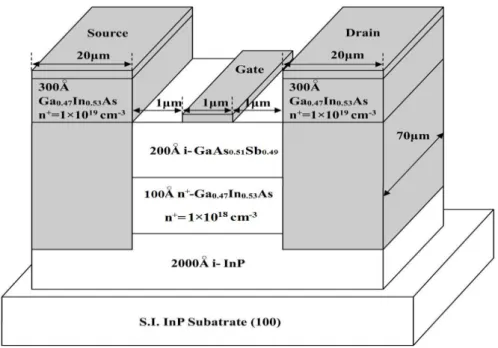
2.2 Device Structure and Experiments
The studied metamorphic co-integrated InP/InGaAs BiFETs with In0.65Ga0.35As pseudomorphic B-E spacer and doping channel layers were grown on an (100) oriented semi-insulating GaAs substrate by molecular beam epitaxy (MBE) system. The epitaxial structures consisted of a 1.5 μm undoped InxGa1-xP (x:0.52→1) metamorphic buffer layer, a 0.15 μm undoped
InP layer, a 0.35 μm n+=1×1019cm-3In
0.53Ga0.47As subcollector layer, a 0.5 μm n - =5×1016cm-3 In
0.53Ga0.47As collector layer, a 0.1 μm p+=1×1019cm-3 In0.53Ga0.47As base layer, a 50 Å i-In0.65Ga0.35As spacer layer, a n+=2×1012cm-2 δ-doped sheet, a 50 Å i-In0.65Ga0.35As spacer layer, a 0.1 μm n=5×1017cm-3 InP emitter layer, a 0.3 μm n+=1×1019cm-2 In
0.53Ga0.47As emitter cap layer, a 0.2 μm i-InP separated layer, a 150 Å n+=3×1018cm-3 In
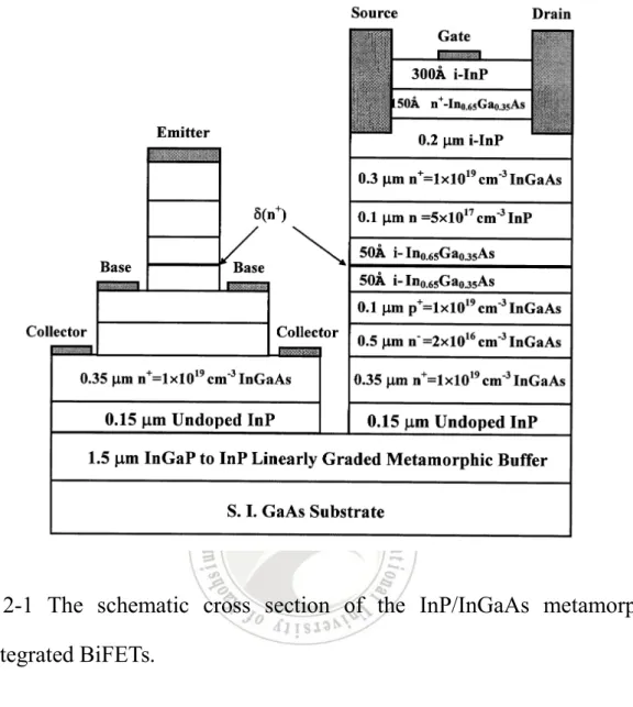
0.65Ga0.35As doping channel layer, a 150 Å i-InP gate layer, and a 300 Å n+=1×1019cm-3 In0.53Ga0.47As drain and source cap layer. In the device process, the top four layers of the structure were first removed by chemical wet selectively etching techniques for the fabrication of the HBT. Then, the emitter self-aligned mesa was formed and etched to base layer. After the deposition of AuZn base metal, the base mesa was defined and formed by etching the base and collector layers. Then, AuGaNi metal was deposited on the HBTs sub-collector layer as well as FETs drain and source regions, simultaneously. The above ohmic contacts were formed by sintering at 450 °C for 30 s. Subsequently, the device mesa was formed to provide the isolation between the HBT and FET. Finally, the gate region was defined and recessed by selectively etching the n+-InGaAs cap layer, and then Schottky contact was formed on the i-InP gate layer by evaporating and lifting off the Au metal. The schematic cross section of the InP/InGaAs metamorphic co-integrated BiFETs is shown in Figure 2-1. The emitter and gate dimensions are 50×50 and 1×100 μm2 in the HBT and FET, respectively.
Fig. 2-1 The schematic cross section of the InP/InGaAs metamorphic co-integrated BiFETs.
2.3 Experimental Results and Discussion
For the studied InP/InGaAs FET with an In0.65Ga0.35As pseudomorphic quantum-well doping channel, it was constructed on the material layers of the metamorphic HBT. At thermal equilibrium, the corresponding energy band diagram of the FET is depicted in Fig. 2-2. Due to the considerable Ec value at InP/In0.65Ga0.35As heterojunction and the employment of a thin as well as heavily doped In0.65Ga0.35As channel between two undoped InP layers, it will
form a large potential barrier preventing the electron injection from channel into gate electrode and a wide gate operation voltages could be expected.
Fig. 2-2 Corresponding energy band diagram of the InP/InGaAs FET with In0.65Ga0.35As pseudomorphic doping channel grown on the metamorphic HBT at equilibrium.
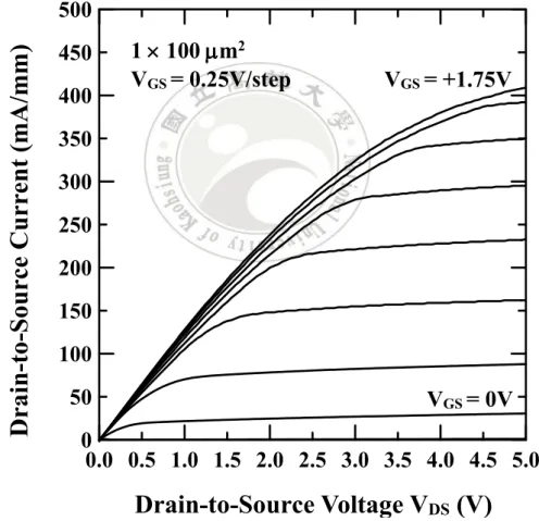
Figure 2-3 illustrates the measured three-terminal current-voltage (I-V) characteristics of the studied FET. The device exhibits a maximum drain current of 409 mA/mm at VGS = +1.75 V. The large gate forward operation voltage could be attributed to the relatively large gate potential barrier height
0.05 0.15 0.00 0.10 0.20 -1.2 -1.0 -0.8 -0.6 -0.4 -0.2 0.0 0.2 0.4 0.6 0.8 1.0 E n er gy B an d (e V ) Coordinate Position (m) Gate i-InP n+-In0.65Ga0.35As i-InP Ec Ev
with utilizing a small energy-gap In0.65Ga0.35As doping channel. In addition, there is not apparent buffer current observed even at VGS = –0.25 V and VDS = +5 V. Accordingly, the sufficiently large Ec value at InP/In0.65Ga0.35As heterojunction can effectively improve the buffer leakage current than the convention InP/In0.53Ga0.47As FET. Hence, the excellent FET performance can be without growing a heterojunction buffer layer or a buried p-layer on the buffer layer.
Fig. 2-3 Measured three-terminal current-voltage characteristics of the studied InP/InGaAs FET with In0.65Ga0.35As pseudomorphic doping channel.
0.5 1.5 2.5 3.5 4.5 0.0 1.0 2.0 3.0 4.0 5.0 50 150 250 350 450 0 100 200 300 400 500 1 100 m2 VGS= 0.25V/step VGS= +1.75V VGS= 0V
D
ra
in
-t
o-S
ou
rc
e
C
u
rr
en
t
(m
A
/m
m
)
Drain-to-Source Voltage V
DS(V)
Figure 2-4 illustrates the drain saturation current and transconductance versus the gate-to-source voltage at VDS = 5 V. The maximum drain current and threshold voltage are of 409 mA/mm and –0.25 V, respectively. The FET exhibits a maximum transconductance as high as 312 mS/mm. In particular, it exhibits good device linearity, i.e., voltage-independent transconductance, attributed to the excellent confinement effect for electrons in channel by the employment of a thin and heavy-doped In0.65Ga0.35As quantum-well channel between two thin InP undoped layers.
Fig. 2-4 Transconductance and drain saturation current as a function of gate-to-source voltage of the studied InP/InGaAs FET with In0.65Ga0.35As pseudomorphic doping channel.
1 100 m2 VDS= 5V
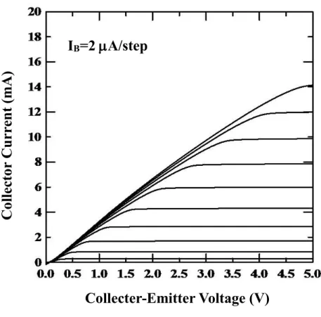
D ra in -t o-S ou rc e C u rr en t (m A /m m ) T ra ns co n d u ct an ce (m S /m m ) Gate-to-Source Voltage VGS(V)After removing the top four layers of structures, the studied HBT was fabricated on the metamorphic buffer layer. Fig. 2-5(a) shows the common-emitter I-V characteristics of the HBT. The base current is biased by 2 A/step. As seen in the figure, a maximum collector current of 14.1 mA at VCE = 5 V is obtained and there is not apparent Early effect. The enlarged view of the I-V characteristics near the small collector-emitter (C-E) region is depicted in Fig. 2-5(b).
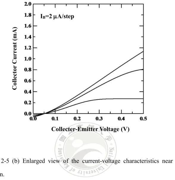
Fig. 2-5 (a) Common-emitter current-voltage characteristics of the metamorphic HBT. IB=2A/step C ol le ct or C u rr en t (m A ) Collecter-Emitter Voltage (V)
Fig. 2-5 (b) Enlarged view of the current-voltage characteristics near the origin.
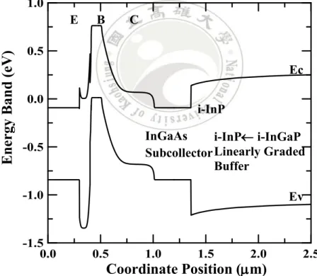
In particular, a relatively small C-E offset voltage of only 50 mV is observed at base current of 2 A, as seen in the figure. The corresponding energy band diagram of the HBT including the InxGa1-xP metamorphic graded buffer layer is depicted in Fig. 2-6(a). The InP/InGaAs material system is formed on the InxGa1-xP to InP linearly graded buffer layer. Figure 2-6(b) shows the enlarged view of energy band diagram near the base-emitter (B-E) region in the studied HBT. In this figure, the potential spike at B-E junction can be entirely eliminated and the confinement effect for hole is effectively
IB=2A/step C ol le ct or C u rr en t (m A ) Collecter-Emitter Voltage (V)
increased due to the employment of a delta-doped sheet between two undoped In0.65Ga0.35As spacer layers to lower the energy band at emitter side. It is worthy to note that the employment of In0.65Ga0.35As spacer layers at B-E junction can further extend EV value at InP/In0.65Ga0.35As heterojunction than that at InP/In0.53Ga0.47As heterojunction. Therefore, a considerably high current gain could be obtained as compared with the reported InP/In0.53Ga0.47As metamorphic HBT [93]. On the other hand, the low VCE value is due to the elimination of potential spike at B-E junction.
Fig. 2-6 (a) Corresponding energy band diagram of the InP/InGaAs metamorphic HBT with In0.65Ga0.35As pseudomorphic spacers at base-emitter junction at equilibrium. 0.0 0.5 1.0 1.5 2.0 2.5 -1.5 -1.0 -0.5 0.0 0.5 1.0 E B C i-InP i-InGaP Linearly Graded Buffer i-InP InGaAs Subcollector Coordinate Position (m) E n er gy B an d (e V ) Ec Ev
Fig. 2-6 (b) Enlarged view of energy band diagram near base-emitter region.
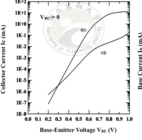
Figure 2-7 depicts the Gummel plots at VBC = 0V. A maximum current gain of 345 is obtained. To our knowledge, the current gain and offset voltage are the best than that of the previous InP/InGaAs metamorphic HBT [91]. The current gain is close to unity when a small base-emitter voltage of 0.3V is biased. Also, the current gain up to 161 is obtained at collector current of 1mA. The ideality factor nC for collector current is nearly equal to unity at low current level. This means that the potential spike at B-E junction has been completely eliminated and the diffusion mechanism dominates the electron transport across the B-E heterojunction. On the other hand, the ideality factors
0.37 0.39 0.41 0.43 0.36 0.38 0.40 0.42 0.44 -1.25 -0.75 -0.25 0.25 0.75 -1.50 -1.00 -0.50 0.00 0.50 1.00 Emitter n-InP (n+) i-In0.65Ga0.35As Base p+-In 0.53Ga0.47As Ec Ev E n er gy B an d (e V ) Coordinate Position (m)
nbfor base current are equal to 1.89 and 1.71 at 0.2V < VBE< 0.35V and 0.4V < VBE < 0.55V, respectively. This means that the recombination mechanism dominates the base current in the metamorphic HBT with psedomorphic In0.65Ga0.35As spacers. As compared with the previous metamorphic HBT without the psedomorphic In0.65Ga0.35As spacers, the studied device exhibits somewhat lower nb value because the In0.65Ga0.35As spacer layers have smaller spacer recombination velocity than the In0.53Ga0.47As spacer layers near the B-E junction.
Fig. 2-7 Gummel plots of InP/InGaAs metamorphic HBT with In0.65Ga0.35As pseudomorphic spacers at base-emitter junction.
VBC= 0 C ol le ct or C u rr en t Ic (m A ) B as e C u rr en t IB (m A ) Base-Emitter Voltage VBE(V)
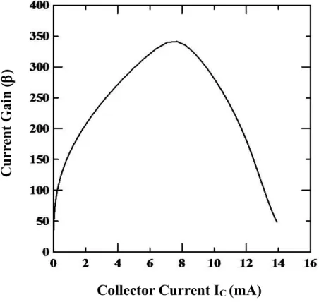
The relationship between collector current and current gain of the studied InP/InGaAs metamorphic HBT is illustrated in Fig. 2-8. At low collector current levels of 0.1 and 1 mA, the current gains are up to 75 and 160, respectively, for the elimination of potential spike at B-E junction.
Fig. 2-8 The relationship between collector current and gain for the studied InP/InGaAs metamorphic HBT with In0.65Ga0.35As pseudomorphic spacers at base-emitter junction.
As compared with the related reports [88,91,93], the studied InP/InGaAs metamorphic co-integrated BiFETs on GaAs substrate show better device
C u rr en t G ai n ( )
performance by the employing of a thin In0.65Ga0.35As pseudomorphic quantum-well channel layer to increase gate forward operation voltage, drain current, and transconductance in the FET, and the use of a delta doping layer between two In0.65Ga0.35As pseudomorphic spacer layers at emitter side to reduce the collector-emitter offset voltage and enhance the current gain in the HBT.
2.4 Summary
In summary, the InP/InGaAs metamorphic co-integrated stacked BiFETs with In0.65Ga0.35As pseudomorphic B-E spacer and doping channel layers grown on the low-cost GaAs substrate have successfully fabricated and demonstrated. Due to the large conduction band discontinuity at InP/In0.65Ga0.35As for the use of a thin In0.65Ga0.35As pseudomorphic quantum-well channel layer, the large gate forward operation voltage, drain current, and transconductance are obtained in the FET. On the other hand, the larger valence band discontinuity at InP/In0.65Ga0.35As heterojunction enables the collector current and current gain to increase in the HBT. Also, based on the design of a -doping sheet between two In0.65Ga0.35As spacer layers, a relatively low collector-emitter offset voltage is achieved. Consequently, the co-integrated metamorphic devices show a good potential for mixed signal integrated circuit and system applications.
Chapter 3
Comparative Investigation of GaAsSb/InGaAs Type-II
and InP/InGaAs Type-I Doped-Channel Field-Effect
Transistors
3.1 Introduction
Over the past years, InP/InGaAs heterostructure field-effect transistors (HFETs) have been considered to be the promising devices in microwave and optoelectronic integrated circuits because of the high electron mobility, large peak saturation velocity in the InGaAs channel layer, and good selective etching between InP and InGaAs materials [13,93].
Recently, heterostructure field-effect transistors (HFETs), such as metal-semiconductor field-effect transistors (MESFETs) [94,95], high electron mobility transistors (HEMTs), and doped-channel field-effect transistors (DCFETs) [78,96], etc., have attracted considerable attention for microwave and digital circuit applications, due to the high current handling capability and high speed operation. In MESFETs, the high field around the metal-semiconductor interface causes the poor gate Schottky behavior. This will induce large gate leakage current, low breakdown voltage, and low gate turn-on voltage. Furthermore, the output drain current and gate voltage swing are low. Another, the HEMT uses the quantum well method, in which the
electron mobility is enhanced. The electron mobility direction is confined in the two-dimensional direction. The confinements cause the electron to be limited at conduction band discontinuity and then the two-dimensional electron gas (2DEG) to be formed. Because the electron can only transport in two-dimension direction, the operation speed is increased when the electron mobility is enhanced. However, the parallel conduction effect is generally found in the traditional HEMTs, it suffered from poor device linearity and low output current [97]. The device performance will be degraded. For the DCFETs, it have been demonstrated to achieve better device linearity and high current drivability. A large energy-gap undoped (or low-doped) materia layer was employed as gate Schottky barrier layer to increase the gate turn-on voltage and enhance the drain current [93]. With respect to the InP/In0.53Ga0.47As type-I heterojunction material system, the DCFETs with a conduction band discontinuity ( Ec ~ 0.23 eV) value at the heterojunction can provide good carrier confinement effect in channel to achieve high gate forward bias, high drain output current, and broad gate voltage swing, simultaneously [98]. Recently, InP/GaAsSb type-II material system has been a new alternative for InP-based double heterojunction bipolar transistors (DHBTs) [99]. In the structures, the current blocking effect could be completely eliminated attributed that the conduction band edge of GaAsSb base layer lies above that of the InP emitter layer.
substrate is first demonstrated. As compared with the conventional InP/InGaAs type-I DCFET, the GaAsSb/InGaAs type-II DCFET with a large Ec value shows a larger transconductance value and a higher drain current. The device mechanism of GaAsSb/InGaAs and InP/InGaAs DCFETs will be demonstrated and compared in detail.
3.2 Device Structures
The device structure of the studied GaAsSb/InGaAs DCFET (labeled device A) includes a 2000 Å undoped InP buffer layer, a 100 Å n+= 1 × 1018 cm−3 In
0.53Ga0.47As channel layer, a 200 Å undoped GaAs0.51Sb0.49 gate layer and a 300 Å n+ = 1 × 1019 cm−3 In
0.53Ga0.47As cap layer. For comparison, another InP/InGaAs DCFET (labeled device B) has the similar structure as the device A except that a 200 Å undoped InP gate layer is employed to replace the GaAsSb layer. A two-dimensional (2D) semiconductor simulation package SILVACO was used to analyze the energy band, distributions of electrons, and dc performance of the two devices [100]. The 2D analysis takes into account the Poisson equation, continuity equation of electrons, Shockley-Read-Hall (SRH) recombination, Boltzmann statistics, and Fermi-Dirac statistics, simultaneously. The gate dimension and spacer of the drain-to-source were 1 × 70 μm2 and 3 μm, respectively. The schematic cross section of the device A and device B are depicted in Figs. 3-1(a) and 3-1(b), respectively.
Fig. 3-1 (a) The schematic cross section of the device A.
3.3 Results and Discussion
The energy bands of the devices A and B before the junction is formed are illustrated in Fig. 3-2.
Fig. 3-2 The energy bands of the devices A and B before the junction.
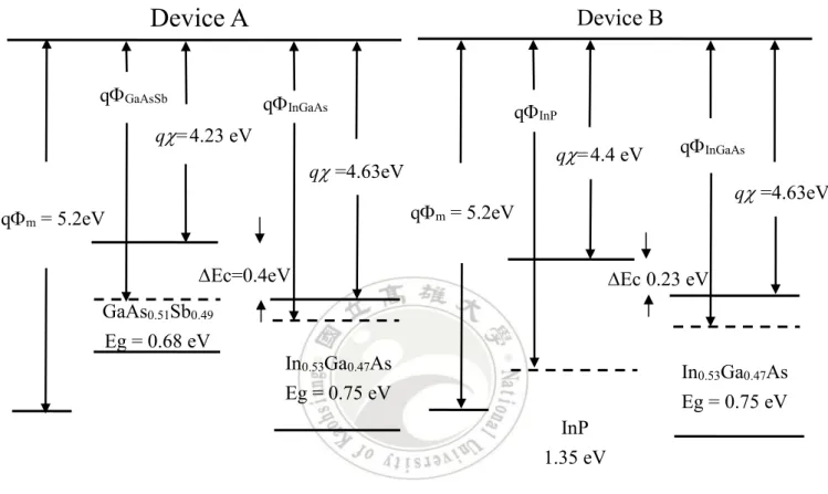
The electron affinities (energy-gap) of GaAs0.51Sb0.49, In0.53Ga0.47As, and InP materials are of 4.23 (0.68), 4.63 (0.75), and 4.4 (1.35) eV, respectively [101]. Apparently, the GaAs0.51Sb0.49/In0.53Ga0.47As and InP/In0.53Ga0.47As heterojunctions form the type-II and type-I heterostructures, respectively.
Device A
Device B qm= 5.2eV qGaAsSb GaAs0.51Sb0.49 Eg = 0.68 eV q=4.23 eV Ec=0.4eV In0.53Ga0.47As Eg = 0.75 eV qInGaAs q=4.63eV qm= 5.2eV InP 1.35 eV qInP q=4.4 eV In0.53Ga0.47As Eg = 0.75 eV Ec 0.23 eV qInGaAs q=4.63eVFurthermore, the Ec value at GaAs0.51Sb0.49/In0.53Ga0.47As heterojunction is estimated to be 0.4 eV, which is higher than that of 0.23 eV at InP/In0.53Ga0.47As heterojunction. The corresponding energy band diagrams at equilibrium and at gate-to-source forward voltage of +0.75 V for the devices A and B are depicted in Figs. 3-3(a) and 3-3(b), respectively.
Fig. 3-3 (a) The corresponding energy band diagrams at equilibrium and at gate-to-source forward voltage of +0.75 V for the devices A.
0.05 0.15 0.25 0.00 0.10 0.20 -1.25 -0.75 -0.25 0.25 0.75 -1.50 -1.00 -0.50 0.00 0.50 1.00 i-GaAsSb Device A at VGS= 0V at VGS= 0.75V EC EV i-InP n+-InGaAs Gate
E
n
er
gy
B
an
d
(e
V
)
Coordinate Position (μm)
Fig. 3-3 (b) The corresponding energy band diagrams at equilibrium and at gate-to-source forward voltage of +0.75 V for the devices B.
When compared with the device B, for the the considerable work function difference (qm >> qGaAsSb) between Au metal and GaAs0.51Sb0.49 layer, it will form a relatively large potential spike at the metal-semiconductor junction in the device A. It is worthy to note that at thermal equilibrium the conduction band of the n+-In
0.53Ga0.47As channel is lower than the Fermi level because the conduction band discontinuity (ΔEc ~ 0.4 eV) at GaAs0.51Sb0.49/In0.53Ga0.47As heterojunction is enough large. Therefore, 2DEG will be formed in the n+-In Ga As quantum-well channel and the device A
0.05 0.15 0.25 0.00 0.10 0.20 -1.25 -0.75 -0.25 0.25 0.75 -1.50 -1.00 -0.50 0.00 0.50 1.00 Device B EC EV i-InP at VGS= 0V at VGS= 0.75V n+-InGaAs i-InP Gate