國立交通大學
材料科學與工程學系
博士論文
探討奈米粒子對 PS-b-P4VP 雙塊式高分子之
影響與 PS-b-P4VP 雙塊式高分子薄膜應用於
記憶體元件
The Effect of Sequestered Nanoparticles on the
Morphologies of Poly(styrene-b-4-vinylpyridine) and
a Poly(styrene-b-4-vinylpyridine) Thin Film Based
Memory Device
研究生: 黃清茂
指導教授: 韋光華 博士
探討奈米粒子對 PS-b-P4VP 雙塊式高分子之影響與
PS-b-P4VP 雙塊式高分子薄膜應用於記憶體元件
The Effect of Sequestered Nanoparticles on the Morphologies of
Poly(styrene-b-4-vinylpyridine) and a Poly(styrene-b-4-
vinylpyridine) Thin Film Based Memory Device
研 究 生:黃清茂 Student: Ching-Mao Huang
指導教授:韋光華 博士 Advisor: Dr. Kung-Hwa Wei
國立交通大學
材料科學與工程研究所
博士論文
A Thesis
Submitted to Department of Material Science and Engineering College of Engineering
National Chiao-Tung University in Partial Fulfillment of the Requirements
for the Degree of Doctor of Engineering
in
Material Science and Engineering December 2008
Hsinchu, Taiwan, Republic of China
Abstract
In this dissertation, we used in situ annealing small-angle X-ray scattering (SAXS) to monitor the structural evolution of a spherical poly(styrene-b-4- vinylpyridine) diblock copolymer (PS-b-P4VP)/2-phenylethanethiol-coated Au nanoparticle (NP) mixture in the solid state during its thermal annealing. We found that the Au NPs that existed initially in a random state with some cluster packing in the PS domain diffused to the interface of the amphiphilic PS-b-P4VP diblock copolymer within 4 h at 170 °C under vacuum to form NP-filled shell-like assemblies, as evidenced from transmission electron microscopy and anomalous SAXS. The Au NP nano-shell assemblies were stable even after redissolving in toluene.
Furthermore, we found that two kinds of NPs—hydrophilic pyridine-coated CdSe NPs and hydrophobic dodecanethiol-coated Au NPs—collectively self- assemble in the PS and P4VP blocks, respectively, of a lamellar PS-b-P4VP diblock copolymer to form a pseudo-tetragonal single-crystalline structure as evidenced from SAXS. The formation of a tetragonal-like single crystal results from micelle structures possessing strong hydrophilic P4VP/CdSe cores and hydrophobic PS/Au coronas that prevented the cores from forming the randomly oriented lamellar domains. Instead, the composite microphase separated into a long-range-ordered structure.
Finally, we reported the performance of a nonvolatile memory device based on a solution-processed PS-b-P4VP thin film. The Al/PS-b-P4VP/ITO memory device featuring metal-coordinated 30-nm-diameter P4VP cores exhibited an ON/OFF ratio of 2×10⁵, an erase voltage of 0.75 V, a write voltage of –0.5 V, and a retention time of 104 s. The device exhibited metallic behavior in the ON state, suggesting the formation of metallic filaments through the migration of Al atoms into the P4VP domain during writing. Such nanostructured diblock copolymer thin films open up new avenues for fabricating organic memory devices using simple procedures.
摘要
此論文主旨為利用小角度散射技術來偵測球狀 PS-b-P4VP 雙塊式共聚高分 子/苯乙基硫醇-Au 奈米粒子複合材料於熱處理期間的結構演進。研究結果發現 Au 奈米粒子起初以具部分團簇隨機地分佈在 PS 相中,經過 170°C 真空下熱處 理4 小時後,由電子顯微鏡與 anomalous 小角度散射觀察得知,Au 遷移至 PS 與 P4VP 的界面,進而形成一層包覆在 P4VP 球外的 Au 殼排列。此結構更被證實 是可以穩定的以PS-Au-P4VP 微胞結構保存於甲苯中。 接著,本論文進一步探討分別將親水性的CdSe 奈米粒子與疏水性的 Au 奈 米粒子先後操控置入P4VP 與 PS 相中。利用 2-D SAXS 鑑定發現在含有適當的 CdSe 與 Au 體積分率的 PS-b-P4VP/CdSe/Au 三元複合材料,會使原本為層狀結 構之PS-b-P4VP 轉變為擬四方體單晶結構。此一相轉變乃由於 CdSe 與 Au 奈米 粒子分別置入 P4VP 與 PS 後造成內聚更強的 P4VP/CdSe 核與較鬆散的 PS/Au 殼,導致溶劑移除後PS-b-P4VP/CdSe/Au 能以穩定的微包結構取代融合回層狀而 存在於固相中,並以溶劑退火(solvent annealing)後堆疊成擬四方體單晶結構。 最後,本論文利用柱狀PS-b-P4VP雙塊式共聚高分子製備可靠的(reliable)有 機非揮發性記憶體。Al/PS-b-P4VP/ITO元件乃由溶液製程在ITO基材上旋轉塗佈 30奈米厚且具六方堆積(hexagonal)奈米結構之PS-b-P4VP薄膜,並蒸鍍Al為上電 極。此一新穎的有機非揮發性記憶體on/off ratio可以達到2×10⁵,寫入和抹除的時間可達到微秒(us)的狀態,且有超過104秒的資料保存時間(retention time)與推估
可使用長達10年以上。根據Al/PS-b-P4VP/ITO元件於On-state下的變溫I-V曲線特 性分析,元件之電流隨溫度下降而上升,代表導電行為似金屬特性。因此,判定 所屬的記憶機制應為金屬導線(metallic filament)。利用此具奈米結構的雙塊式共 聚高分子薄膜,經由簡單的溶液製程製備有機記憶體元件,將提供一條新的有機 非揮發性記憶體製程途徑。
誌謝 感謝上天,感謝交大校門前的土地公,終於到可以寫誌謝的時候了。回首過 去博班一千多個日子裡,往事歷歷在目。這一路走來,有笑、有淚,但更多時候 卻是笑中含淚、淚中帶笑的。時至今日,雖然完成了這部論文,但人生的挑戰卻 正要開始。此時此刻,僅以本篇表達我的誠摯謝意。 首先要先感謝的是指導教授韋光華老師提供舒適的研究環境,並且在溝通上 猶如父親般的包容、在生活上配予優厚的薪水、在研究上給予適時叮嚀與指導。 才讓我得以汲取到豐富歷練,對往後的人生更有信心。也感謝在論文研究過程中 給予我極大幫助的鄭有舜博士,正是他讓我的所做出來的材料,在小角度散射的 光芒下點石成金。另外,也感謝陳信龍教授、許鉦宗教授、何榮銘教授、陳貞夙 教授百忙之中挪空擔任口試委員,並在口試期間提供許多寶貴的建議。這些師長 的鼓勵,是我對研究繼續充滿著熱情的主要動力。 實驗室畢業的學長家充、帥帥、良祐、Mickey、小猪、孝蔚、中斌、老周, 感謝你們讓我看到畢業後美好,讓我能夠持續朝著這個目標來邁進。還有實驗室 的夥伴們:初為人父的振嘉學長、堅毅不拔卻為人親切的耀德、善於分析且為國 道小霸王的旭生、認真負責的長跑健將茂源、老大不小仍體重不減稚氣的冠宇、 純真自然卻有公路殺手稱號的碩麟、認份執著又善良可愛的阿川、XX很扁卻又 肚子很凸的果子吟、好人一枚並努力不懈的阿閔、宅男代表會主席的明鑫、陽光 男孩協會理事長的璨丞、台妹代表暱稱鞭炮串阿鬼的璽夷、寒冰掌高手的俠女秉 萱、無聲無息碩二男雙的小藍與宗諭、熱心又負責忽寬忽細的助理克瑜、以及新 進成員阿川二代─昌隆、建銘&柏宇賢伉儷、比我還捲的曜璿、小扁阿鬼傳人─ 慧妮&毓倩。正因為這群可愛又可惡的污水,讓我這股清流也跟著一起淪陷,時 時刻刻快快樂樂的聊八卦、討論news paper。感謝這群夥伴,沒有你們的一路相 陪,我也就沒辦法有機會生出這篇誌謝。 最後,僅以本論文獻給我最親愛的母親、父親、岳母、妻子芝佑、女兒靖芸 以及十二位哥哥嫂嫂姊姊姐夫,感謝他們在我求學的期間給予精神上及生活上的 協助與支持,使我無後顧之憂得以順利完成學業。 黃清茂 2008.12.12
Table of Contents
Abstract ... Ⅰ 摘要... Ⅱ 誌謝... Ⅲ Chapter 1: Introduction 1-1 Block Copolymers ...1 1-2 Nanoparticles...131-3 Block Copolymer/Nanoparticle Mixtures...16
1-4 Organic Electrical Bistable Memory Device ...24
1-5 Motivation and Scope of Dissertation ...26
Chapter 2: Structural Evolution of Poly(styrene-b-4-vinylpyridine) Diblock Copolymer/Gold Nanoparticle Mixtures from Solution to Solid State 2-1 Introduction...52
2-2 Methods and Analysis...53
2-3 Results and Discussions ...56
2-4 Conclusions ...65
Chapter 3: Pseudo-Single-Crystalline Self-Assembled Structure Formed from Hydrophilic CdSe and Hydrophobic Au Nanoparticles in the Poly(4-vinylpyridine) and Polystyrene Blocks, Respectively, of a Polystyrene-b-Poly(4-vinylpyridine) Diblock Copolymer 3-1 Introduction ...78
3-2 Methods and Analysis ...79
3-3 Results and Discussions ...83
3-4 Conclusions ...88
Chapter 4: Electrical Bistable Memory Device Based on a Poly(styrene-b-4- vinylpyridine) Nanostructured Diblock Copolymer Thin Film 4-1 Introduction ...101
4-2 Methods and Analysis ...102
4-3 Results and Discussions ...103
4-4 Conclusions ...105
Chapter 6: Future Work...112
References...113
Appendix 1: Quantitative calculations of Au NPs at the surface of a single P4VP domain...124 Appendix 2: Distance between the CdSe particles in a single P4VP domain
...125
List of Figures
Chapter 1: Introduction
Figure 1-1 Schematic phase diagram illustrating the various “classical” block copolymer morphologies adopted by linear diblock copolymers ...28 Figure 1-2 Schematic representation of the morphologies of linear ABC triblock
copolymers. The combination of the block sequence (ABC, ACB, BAC), composition, and block molecular weights provides an enormous parameter space for the creation of new morphologies ...29 Figure 1-3 Well-established structures of block copolymers in the melt, solution, or
solid state ...30 Figure 1-4 Phase diagram of a self-assembled diblock copolymer. S: spherical; C:
cylindrical; G: gyroidal; L: lamellar; Scp: closed-packed spherical structure
...31 Figure 1-5 Possible configurations of lamellae in block copolymer films. (a)
Confined at one surface. (b) Confined at both surfaces...32 Figure 1-6 Thin film morphology of an asymmetric block copolymer that forms
hexagonal morphologies in the bulk...33 Figure 1-7 Schematic representation of various applications of block copolymers in
nanotechnology...34 Figure 1-8 Schematic representation of the production process of a metal nanodot
array using block copolymer lithography ...35 Figure 1-9 SEM image of a polystyrene-b-polyferrocenyldimethylsilane mask after
removal of the polystyrene through O2 RIE ...36
Figure 1-10 Schematic representation of selectively distributed TiO2 NPs in a
PS-b-PMMA diblock copolymer ...37 Figure 1-11 (a) Assembly of Au NPs (core: 3.9 ± 1.0 nm; shell: PS; core + shell = 7.7
nm) into PS-b-P4VP. (b) Assembly of Au NPs (core: 3.9 ± 1.0 nm; shell: PS and P2VP; core + shell = 7.7 nm) into PS-b-P4VP. (c, d) Respective
histograms of particle locations for the samples displayed in (a) and (b) ...…38 Figure 1-12 (a) Schematic of synthesis of needle-like TiO2 nanostructures with
ordered patterns. (b) The cross-section SEM image of needle-like TiO2. ..
...39 Figure 1-13 SEM image of an etched polystyrene-b-polyisoprene diblock, revealing a
fracture surface. The polystyrene network channels remaining after removal of polyisoprene are clearly visible ...40 Figure 1-14 Density functional theory calculations of large (case 1) and small NPs
(case 2). The NPs are either located at the center of the A phase (case 1) or driven closer to the A–B interface (case 2)...41 Figure 1-15 Cross-sectional transmission electron micrograph displaying Au NPs
patterned within the P4VP lamellae formed by a PS-b-P4VP diblock copolymer ...42 Figure 1-16 TEM image of an array of Fe2O3 NPs and 1-dodecanethiol-coated Au
NPs in a PS-b-P4VP matrix after removal of the polymer matrix through O2 plasma treatment. The inset displays an enlarged view of Au NPs at the
PS–PVP interface; the iron oxide NPs are centered in the former PVP phase ...43 Figure 1-17 (a) NPs (CdSe–TOPO; R = 5 nm) deposited into a block copolymer
template [PS–PMMA (70:30)] through withdrawal of the template from solution. (b) TEM image of the resulting film; the NPs are located inside the (black) holes...44 Figure 1-18 Deposition of Au NPs (R = 2.5 nm) via directed hydrogen bonding
interactions onto a film consisting of a block copolymer ...45 Figure 1-19 Morphological transformation from a hexagonally packed cylinder
structure of pure PS-b-P4VP diblock copolymers to lamellar (CdS/P4VP)-b-PS composites ...46 Figure 1-20 TEM micrograph of a ternary blend of PS-b-PEP, AuR1, and SiO2R2
with an inorganic filling fraction (f) of 0:02, recorded after micro-sectioning normal to the layer direction (no stain)...47 Figure 1-21 (a) TEM image of a PS-PEP/AuSC12H25 composite after micro-
sectioning normal to the layer direction, revealing particle deposition at the PS–PEP interface and (b) TEM image of a PS-PEP/AuSPS composite. PEP domains appear as brighter regions in the micrograph. (c) Absorptance spectra of PS-PEP/Au composite materials possessing an interfacial segregated morphology (dotted line) and a selective-layer uniform morphology (continuous line). Inset: Absorptance spectra of dilute nanocrystal solutions [AuSC12H25 (dotted line) and AuSPS
(continuous line)]...48 Figure 1-22 Scaling behavior of the I–V curves of 48% (Au NPs/P4VP)-b-PS and Au
NPs/homo-P4VP at 78 K ...49 Figure 1-23 (a) Molecular structure of the PS-b-P4VP copolymer and a schematic
representation of the micellation process with in situ synthesis of Au NPs in PS-b-P4VP. (b) AFM topographic image of the surface of a spin-coated PS-b-P4VP film along with a schematic illustration of a self-assembled PS-b-P4VP (with Au NPs) micellar film on a substrate. (c) Capacitance–voltage (C–V) measurements at 100 kHz on a metal– insulator–silicon structure with a PS-b-(P4VP/Au) film ...50 Figure 1-24 Typical I–V curves for PVK films. The inset presents the plot of ON- and
OFF-state resistances after reading at 1 V per 100 s. The retention time of the ON and OFF states is more than a time period of 105 s for the PVK films...51
Chapter 2: Structural Evolution of Poly(styrene-b-4-vinylpyridine) Diblock Copolymer/Gold Nanoparticle Mixtures from Solution to Solid State Basic Electron Transport Theory
Figure 2-1 (a) HR-TEM image of AuSC2Ph cast from a toluene solution. (b) The
(dashed curve) using polydisperse spheres of the Schultz distribution (in radius r) shown. ...68 Figure 2-2 Solution SAXS profiles of the as-prepared PS-b-P4VPSph, AuSC2Ph, and
the PS-b-P4VPSph/AuSC2Ph mixture in toluene ...69
Figure 2-3 (a) In situ thermal annealing SAXS profiles of the as-prepared PS-b- P4VP Sph/AuSC2Ph mixture. (b) The SAXS profile of the annealed
PS-b-P4VPSph...70
Figure 2-4 (a) Anomalous SAXS data for the PS-b-P4VPSph/AuSC2Ph film before the
thermal annealing, and (b) Anomalous SAXS data for the thermal annealed PS-b-P4VPSph/AuSC2Ph film at two beam energies of 11.910 and 11.200
keV (near L3-edge absorption of Au)...71
Figure 2-5 (a) TEM image for the as-prepared PS-b-P4VPSph/AuSC2Ph mixture, with
abundant NP clusters. (b) TEM micrograph of the PS-b-P4VPSph/AuSC2Ph
mixture that had been subjected to two-step annealing, 48 h of solvent annealing at 30 °C and 72 h for thermal annealing at 170 °C. Inset: HR-TEM image of a single P4VPSph/AuSC2Ph core/shell assembly...72
Figure 2-6 (a) The TGA result of the PS-b-P4VPSph/AuSC2Ph mixture before and
after 72 h thermal annealing at 170 °C under vacuum. (b) The weight loss (%) vs. the annealing time of the PS-b-P4VPSph/AuSC2Ph mixture during
the 170 °C isothermal annealing under a N2 atmosphere. ...73
Figure 2-7(a) Solution state SAXS profiles of the PS-b-P4VPSph, PS-b-P4VPSph/AuPy,
and PS-b-P4VPSph/AuSC2Ph systems after they had been subjected to
annealing and redissolving in toluene. All schematic micellar structures of PS-b-P4VPSph-Au NP mixtures appear near the corresponding curves. (b)
Three corresponding profiles fitted using the Guinier approximation....74 Figure 2-8 (a) TEM image of a recast thin film of the PS-b-P4VPSph/AuSC2Ph
mixture that had been subjected to annealing. (b) HR-TEM image of a single P4VPSph/AuSC2Ph core/shell assembly...75
P4VP/AuSC2Ph composites (b), the annealed lamellar
PS-b-P4VP/AuSC2Ph composites (c),a and the as-prepared AuSC2Ph NPs
(d)...76 Figure 2-10 N 1s XPS spectra of the pure P4VP (a), the annealed P4VP/AuSC2Ph
composites (b), and the annealed lamellar PS-b-P4VP/AuSC2Ph
composites (c) ...77
Chapter 3: Pseudo-Single-Crystalline Self-Assembled Structure Formed from Hydrophilic CdSe and Hydrophobic Au Nanoparticles in the Poly(4-vinylpyridine) and Polystyrene Blocks, Respectively, of a Poly(styrene-b-4-vinylpyridine) Diblock Copolymer
Figure 3-1 (a) SAXS profiles of PS-b-P4VP, PS-b-P4VP/CdSe NPs (3.3 vol%), and PS-b-P4VP/Au NPs (5.3 vol%). (b–d) Cartoon representations of the structures of the PS-b-P4VP/NP binary composites representing the SAXS profiles in (a)...93 Figure 3-2 TEM images of the (a) PS-b-P4VP/3.3 vol% CdSe NPs and (b)
PS-b-P4VP/5.3 vol% Au NPs binary composites. The insets to (a) and (b) display enlarged partial images...94 Figure 3-3 2D SAXS patterns in the low-Q range (q = 0.06 - 0.2 nm–1) for
PS-b-P4VP/CdSe/Au ternary composites possessing various NP loadings. The contrast for each pattern is independent. ...95 Figure 3-4 2D SAXS patterns in low-Q range (q = 0.06 - 0.2 nm–1) for the
PS-b-P4VP/CdSe/Au composite containing 1.7 vol% CdSe NPs and 5.3 vol% Au NPs. (a, b) The Miller indices are marked according to a tetragonal cell, used to index the diffraction patterns of the ab plane (white), superimposed over the tilted ac (orange) and bc (red) planes. (c) TEM images of PS-b-P4VP/1.7 vol% CdSe NPs/5.3 vol% Au NPs ternary composites revealing the [110] and [001] cell directions of the tetragonal cell. The upper-right-hand inset displays an enlarged image. (d) Corresponding orientation for the TEM images. ...96
Figure 3-5 (a) TEM image of the PS-b-P4VP/1.7 vol% CdSe NP/5.3 vol% Au NP composite. The inset displays the FFT of (a). (b) Reconstructed image (inverse FFT image) from the FFT image taken by the two pairs of FFT spots highlighted in the inset. (c, d) Reconstructed images taken by the single pairs of FFT spots highlighted in the respective insets. ...97 Figure 3-6 (a) TEM image of the PS-b-P4VP/1.7 vol% CdSe NP/5.3 vol% Au NP
composite. EDX spectra recorded from the (b) PS/Au and (c) P4VP/CdSe phases marked by red dashed circles in the enlarged TEM image ...98 Figure 3-7 (a) Azimuthal scanning profile of the image in Figure 3-4b (Q = 0.161
nm–1); the (100), (0-1-1), (-101), (-10-1), (0-1-1), (-100), (01-1), (01-1), (10-1), (101), and (011) reflections are found at values of Ø of 0°, 36°, 65°, 113°, 143°, 180°, 216°, 244°, 293°, and 323°, respectively. (b) SAXS profile obtained along the (101) spot in Figure 3-4b ...99 Figure 3-8 SAXS data for a control experiment employing PS-b-P4VP/CdSe/Au
composites in solution. The PS-b-P4VP/NP composites incorporating 1.7 vol% CdSe NPs and/or 5.3 vol% Au NPs...100
Chapter 4: Electrical Bistable Memory Device Based on a Poly(styrene-b-4- vinylpyridine) Nanostructured Diblock Copolymer Thin Film
Figure 4-1 (a) Morphology of a cylindrical PS-b-P4VP diblock copolymer in the bulk state. (b) Micellar structure of a cylindrical PS-b-P4VP diblock copolymer in a selective solvent. (c) Nonvolatile memory device comprising an active PS-b-P4VP diblock copolymer film and Al and ITO electrodes. (d) SEM image of the cross-section of the memory device in (c). ...106 Figure 4-2 I–V characteristics of PS (
♦
), P4VP (■), and PS-b-P4VP (▲). The turn-oncompliance current was restricted to 10–3 A. The inset displays an AFM topographic image of the PS-b-P4VP thin film prior to evaporating the Al electrode...107 Figure 4-3 Logarithmic I–V plots measured at various temperatures for the ON state
at potentials ranging from 0.01 to 0.2 V. The inset displays the resistance of the ON state plotted with respect to the temperature...108 Figure 4-4 (a) Write/read/erase test of the ITO/PS-b-P4VP/Al organic memory device.
The bottom and top curves represent the applied voltage pulse and the corresponding current response, respectively. (b) Retention times of the ON and OFF states of the ITO/PS-b-P4VP/Al organic memory device probed in terms of the device current after stressing ...109
List of Schemes & Tables
Chapter 2: Structural Evolution of Poly(styrene-b-4-vinylpyridine) Diblock Copolymer/Gold Nanoparticle Mixtures from Solution to Solid State Basic Electron Transport Theory
Scheme 2-1 Fabrication of the Self-Assembled PS-b-P4VP/AuSC2Ph Bulk Film···
··· 66 Scheme 2-2 Schematic Representation of the Structural Evolution of the
PS-b-P4VPSph/ AuSC2Ph Mixture at Various Annealing Times. ··· 67
Chapter 3: Pseudo-Single-Crystalline Self-Assembled Structure Formed from Hydrophilic CdSe and Hydrophobic Au Nanoparticles in the Polystyrene and Poly(4-vinylpyridine) Blocks, Respectively, of a Poly(styrene-b-4-vinylpyridine) Diblock Copolymer
Scheme 3-1 Schematic Representation of the Method of Preparation of the
PS-b-P4VP/ CdSe/Au Ternary Composites... ...90 Scheme 3-2 Formation of Tetragonal Crystals from PS-b-P4VP/CdSe/Au Ternary
Composites...91 Table 3-1 Average center-to-center (D) and edge-to-edge (d) interparticle distances.
The schematic representation of the cubic lattice model for the free volume per CdSe dot in a single P4VP domain ...92
Chapter 1
Introduction
1-1 Block Copolymers
Block copolymers are polymers composed of blocks of two or more different homopolymers joined together by covalent bonds in a variety of architectures. The most important characteristics for defining block copolymers are the
(1) weight- (Mw) and number-average (Mn) molecular weights of the block copolymer and its block components;
(2) polydispersity index (PDI), namely the molar mass distribution represented by Mw/Mn;
(3) volume fractions of blocks (f), which characterizes the block copolymer composition; and
(4) Flory–Huggins interaction parameter (χ),[1–3] a measure of the strength of interaction between the blocks.
Block copolymers are versatile platform materials because, at suitable compositions and under appropriate conditions, they can self-assemble into a variety of nanostructures, having period thicknesses between 10 and 100 nm, as a result of microphase separation between incompatible blocks. Block copolymer microphase separation can be described accurately in terms of two competing processes: repulsion of dissimilar monomers and stretching of polymer chains.[4] Incompatibility of blocks drives them to separate into a microdomain structure where the block junctions form microdomain interfaces. Thermodynamically, this process is parameterized by the enthalpy of demixing of polymer blocks (ΔHp). The surface-to-volume
ratio—and, thus, the interfacial free energy—of the block copolymer system decreases as the microdomains increase in size. Because microdomain growth creates a density deficiency toward the microdomain’s center, the block copolymer
chains are stretched beyond the undisturbed Gaussian gyration radius (Rg) to fill the
space. This process, which is accompanied by a reduction of the configurational entropy (ΔSp,conf), opposes the block separation. The additional loss in entropy
ΔSp,intarises from confining the block junctions in the interfacial region. The sign of
the change in Gibbs free energy (Eq. 1-1):
ΔGp = ΔHp−ΔSp,intT−ΔSp,confT (1-1)
indicates whether the transition from a phase possessing homogeneously mixed blocks (disordered state) to an ordered structure is favorable. The transition occurs when the enthalpic part dominates, i.e., ΔGp > 0. The demixing enthalpy (ΔHp) is
proportional to the dimensionless Flory–Huggins segmental interaction parameter χ, which exhibits the following temperature dependence (Eq. 1-2):
χ = a/T + b (1-2)
where a and b are experimentally obtained constants for a given composition of a particular blend pair. Experimentally, χ can be controlled through changes in temperature. The entropy penalty ΔSpis inversely proportional to the total degree of
polymerization (N), defined (for A-B diblock copolymers) as Eq. 1-3:
N = NA+ NB (1-3)
where NA and NBare the average number of monomeric units in blocks A and B,
respectively. Unlike macrophase separation in blends, the connectivity of the blocks in block copolymers prevents complete separation; instead, the diblock copolymer chains organize to place the A and B portions on opposite sides of an interface. The equilibrium nanodomain structure must minimize unfavorable A–B contact without over-stretching the blocks.[1] The product χN expresses the enthalpic/entropic balance—in other words, the degree of microphase separation. The values of χN and the block volume fraction f completely determine the symmetry and dimensions of the microphase-separated structure; they are used for to construct the block copolymer’s
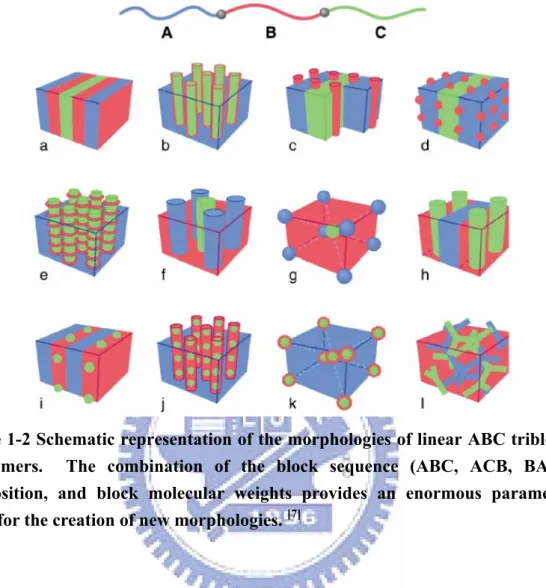
phase diagram. For the simplest class of A-B diblock copolymers, the following structures are known to be stable, as confirmed theoretically[5] and experimentally[2,6]: lamellar, hexagonal-packed cylinder, body-centered cubic, close-packed spherical (which may exhibit only liquid-like ordering), and bicontinuous cubic gyroid structures (Figure 1-1). For ABC triblocks, the combination of two independent composition variables (e.g., the volume fractions fA, fB and fC, where fA + fB + fC = 1)
and three χ parameters (χAB, χAC, and χBC) leads to the much wider range of possible
morphologies presented in Figure 1-2, many of which have been observed, although others await discovery.[7] Theoretical studies have provided guidelines for rationalizing the observed morphologies; in future, they might also be used to predict structures.[8]
1-1-1 Structures of Block Copolymer Melts, Solids, Solutions, and
Thin Films
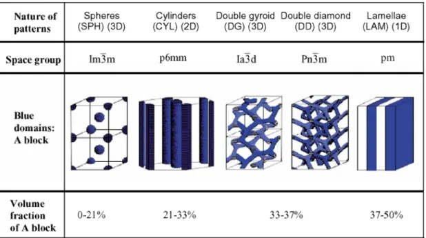
A remarkable property of block copolymers is their ability to self-assemble in the melt into a variety of ordered structures exhibiting nanoscale periodicities. These structures can be controlled by varying the composition of the block copolymer or the segregation between blocks (via the temperature or the degree of polymerization). Figure 1-3 displays the well-established structures of block copolymers in the melt, solution, and solid states.[9]
1-1-2-1 Block Copolymer Melts
Interest in the phase behavior of block copolymer melts stems from the microphase separation of their blocks, leading to nanoscale-ordered morphologies. Two competing effects govern the thermodynamics of block copolymer melts. At high temperatures, the chains are mixed homogeneously, as in any polymer melt. As the temperature is reduced, the tendency for the blocks to segregate is enhanced, i.e.,
the enthalpic process of demixing is favored. This process is, however, necessarily accompanied by a reduction in entropy as the chain configuration becomes more constrained. The extent of segregation of the copolymer may then be expressed using the reduced parameter χN. Here N is the copolymer degree of polymerization, reflecting the N-dependent translation and configuration entropy.
The segment–segment interaction parameter (Flory–Huggins) describes the free energy cost per monomer of conducts between the A and B monomeric units; it is given by (Eq. 1-4):
(
)
[
AB AA BB /2 B AB Zκ T ε ε ε χ ⎟ − + ⎠ ⎞ ⎜ ⎝ ⎛ =] (1-4)
where ε is the interaction energy per monomer unit between the A and B AB monomers and Z is the number of nearest neighbor monomers to a copolymer configuration cell. Thus, a positive value of χAB (which occurs is the vast majority
of cases) represents repulsion between the A and B monomers, whereas a negative value signifies mixing of unlike monomers. Moreover, the value of χAB usually
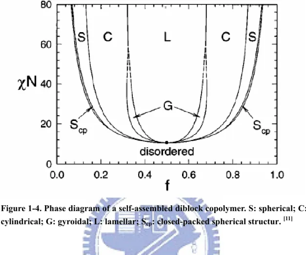
varies inversely with the temperature. The second parameter that strongly influences the block copolymer behavior is the total degree of polymerization, N. For a large value of N, the loss of translational and configurational entropy leads to a reduction of the A-B monomer contacts and, thus, to local ordering. Because the entropic and enthalpic contributions to the free energy scale with respect to N–1 and χ, respectively, the value of the product χN is the most important factor when determining the block copolymer’s phase state.
Figure 1-4 displays a good phase diagram computed using self-consistent mean field theory.[10,11] It reveals the generic sequence of phases accessed just below the order–disorder transition temperature for diblock copolymers of various compositions. The features of the phase diagrams for particular systems different in detail, but
qualitatively they are similar and are well accounted for by self-consistent field (SCF) theory.
1-1-2-2 Block Copolymer Solids
The structures of block copolymer melts are usually trapped upon vitrification. The mechanism underlying the glass transition is similar to those of the constituent homopolymers. Thus, there are few distinct physical factors associated with the formation of solid phases from glassy block copolymers.
In contrast, crystallization of one or both components of a block copolymer is accompanied by profound structural and dynamic changes. The fundamental process in crystallization of chains in a crystallizable block copolymer is the change in block conformation, i.e., the adoption of an extended or folded structure rather than the coiled configuration found in the melt or in solution. Crystallization from the melt often leads to a distinct (usually lamellar) structure having periodicity differing from that in the melt. Crystallization from solution can lead to non-lamellar crystalline structures, although they often possess trapped non-equilibrium morphologies. In addition to the formation of extended or folded chains, crystallization may also lead to gross orientational changes in the structures of the chains.
1-1-2-3 Block Copolymer Solutions
In a solvent, block copolymer phase behavior is controlled by the interaction between the segments of the polymers and the solvent molecules, as well as the interactions between the segments of the two blocks.[12] If the solvent is unfavorable for one block, micelle formation can occur in dilute solution. The phase behavior of concentrated solutions can be mapped onto that of the block copolymer melts (Figure 1-3).[9] There are two basic processes that characterize the phase behavior of block copolymers in solution: micellization and gelation. Micellization occurs when block
copolymer chains associate into (often spherical) micelles in dilute solution in a selective solvent. The core of the micelle is formed by the insoluble or poorly solvated block, whilst the corona contains the selectively solvated block. At a fixed temperature, micellization occurs upon increasing concentration to the critical micelle concentration (CMC). The CMC is usually determined from the sharp decrease in the surface tension as a function of concentration, although other properties, such as viscosity, also exhibit pronounced changes.
In concentrated solutions, micelles can become ordered into gels. Soft and hard gels are distinguished from each other and from micellar solutions by their flow properties—with gels being characterized by a finite yield stress. Hard gels seem to be associated with the formation of cubic phases of spherical micelles, whereas soft gels are usually lamellar or hexagonally packed rod micellar phases. The phase behavior of these materials has only recently begun to be elucidated using small angle scattering. It promises to be even richer than that of block copolymer melts—at least if results for analogous conventional surfactants are any guide. The flow behavior of these gels forms the basis for many of their applications; studies of the rheology and behavior of these materials under shear will enhance the fundamental understanding underpinning future developments.
1-1-2-4 Block Copolymer Thin Films
Microphase separation by block copolymers in thin films has been investigated from several perspectives. First, the physics of self-assembly in confined soft materials can be studied using model block copolymer materials for which reliable mean-field statistical mechanical theories have been developed.[13–16] Second, interest has expanded as a result of the potentially exciting applications that exploit self-organization to (i) fabricate high-density data storage media,[17,18] (ii) lithographically pattern semiconductors exhibiting ultra-small feature sizes,[19,20] and
(iii) prepare ultra-fine filters or membranes.[21] Although research in this field is growing at a rapid pace, the field has not been reviewed since 1998,[2,22] even though many new developments have occurred.
Block copolymer films can be prepared using spin-coating techniques, where drops of a solution of the polymer in a volatile organic solvent are deposited on a spinning solid substrate (silicon wafers are often used because of their uniform flatness). The polymer film spreads as a result of centrifugal forces and the volatile solvent is rapidly driven off. With care, the method can provide films exhibiting low surface roughnesses over areas of several square millimeters. The film thickness can be controlled through modification of the spin speed, the concentration of the block copolymer solution, and the volatility of the solvent, which also influences the surface roughness.[23] Dip coating is another reliable method for fabricating uniform thin films.[24] Whichever deposition technique is used, if the surface energy of the block copolymer is much greater than that of the substrate, dewetting will occur. The mechanism of dewetting has been investigated in some depth.[25–27]
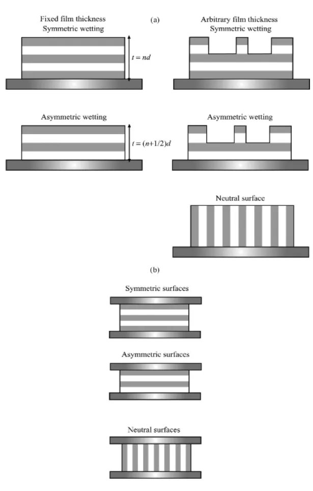
In thin films, the lamellae formed by symmetric block copolymers can be oriented either parallel or perpendicular to the substrate. A number of possible arrangements of the lamellae are possible (Figure 1-5), depending on the surface energies of the blocks and the substrate and whether the film is confined at one or both surfaces. In the case that a different block preferentially wets the interface with the substrate or air, wetting is asymmetric and a uniform film has a thickness (n + 1/2)d. If the initial film thickness is not equal to (n + 1/2)d, then islands or holes (quantized steps of height d) form to conserve volume.[28] As well as leading to distinct orientations, confinement of block copolymers can change the thermodynamics of ordering; in particular, surface-induced ordering persists above the bulk order–disorder transition.[29]
Asymmetric block copolymers that form hexagonal or cubic-packed spherical morphologies in the bulk, form stripe or circular domain patterns in two dimensions, as illustrated in Figure 1-6. The stripe pattern results from cylinders lying parallel to the substrate; a circular domain surface pattern occurs when cylinders are oriented perpendicular to the substrate or when spheres are present at the surface. Because bicontinuous structures cannot exist in two dimensions, the gyroid phase is suppressed in thin films. Nanostructures in block copolymer films can be oriented using electric fields (if the difference in dielectric permittivity is sufficient)—an important property for applications in which parallel stripes[30] or perpendicular cylinder configurations[31] are desired.
1-1-3 Applications
Until recently, most block copolymers have been applied industrially as adhesives or for their mechanical properties (e.g., as thermoplastic elastomers). Only in the past 10 years have researchers taken block copolymers into the area of “high technology,” particularly into the realm of the so-called “nanotechnologies”. Many attempts have been made to use block copolymers in nanotechnology. Self-assembled block copolymer microstructures having dimensions ranging from 10 to 100 nm are useful as nanometer-scale membranes, templates for the fabrication of nano-objects (e.g., metal or ceramic nanodots and wires), as 1-, 2-, and 3D photonic crystals, and as nanopattern masks for the fabrication of high density information storage media. The majority of applications proposed to date rely on the use of thin film structures; this feature is a major focus of the current review, although bulk nanoporous materials and photonic crystals are also considered. Figure 1-7 summarizes the applications of various block copolymer-enabled nanotechnologies.[32]
1-1-3-1 Nanolithography with Self-Assembled Block Copolymer Patterns
Although photolithography has played a dominant role in producing feature sizes smaller than 100 nm, feature sizes of less then 50 nm are not readily obtained using conventional lithography techniques. The minimum size that can be achieved through photolithography is determined by the wavelength of light used in the exposure. Electron beam lithography is commonly used to access feature sizes between 30 and 150 nm. Nevertheless, sizes less than 30 nm are not easy to obtain using standard lithography. One way to overcome this problem is through the use of self-assembled block copolymers.
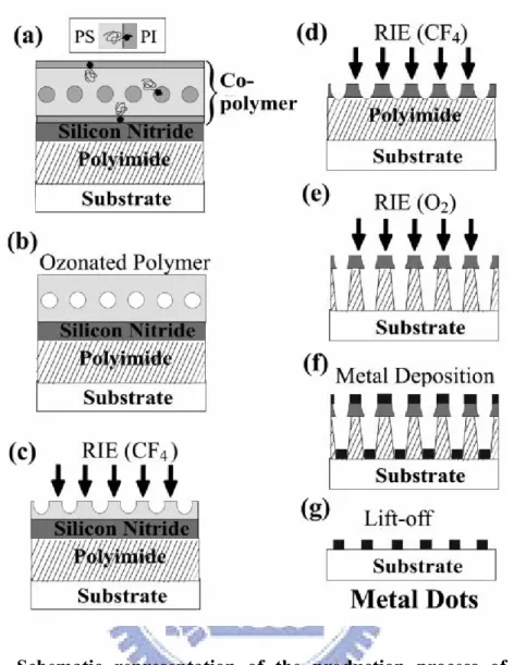
In a pioneering paper, Park et al. demonstrated the use of block copolymer films as masks to transfer dotted and striped patterns into semiconductors.[33] They achieved a feature density of holes of ca. 1011 cm–2. The method they developed relies on the selective ozonation of polyisoprene (PI) or polybutadiene (PB) in block copolymers with polystyrene (PS) as the other (majority) component. Ozone cleaves the olefinic bonds in unsaturated polymers, such that they can be etched away. This process leaves holes or stripes in the PS matrix. This pattern is then transferred from the block copolymer into silicon nitride through reactive ion etching (RIE) using CF4
or CF4/O2 gases. The quality of the pattern transfer is excellent, producing
nanoscale arrays of pits or channels. Park et al. also described how to prepare nanoscale arrays of posts by using an “inverse” mask, relative to that employed to produce the array of pits. If the PI is fixed by staining with osmium tetroxide, then etching of the matrix will occur preferentially. The regions under the PI domains will be left as an array of posts. Details of the ozone etching method for preparing block copolymer film masks were elaborated on in a subsequent paper,[21] which also contains data illustrating pattern transfer into other semiconductors, including silicon and germanium. A patent was awarded for this technology in 1999.[34] In a further
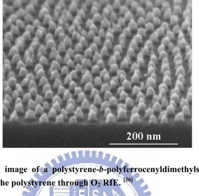
extension of the technique, arrays of nano-sized metal posts have been fabricated using the modified method illustrated in Figure 1-8.[35] A lithographic procedure in which the ozone etching step can be omitted has also been developed;[36] here, the reactive ion etch rate is sufficiently different between the two blocks in the PS-b-PFS (PFS = polyferrocenyldimethylsilane) diblock copolymer, allowing selective etching of PS to occur directly. The technology has been applied to the development of a self-assembly route to produce a high-density magnetic storage medium (in this case, cobalt nanodots). Oxygen plasma RIE leaves PFS spheres; the pattern is then transferred into silicon oxide (which improves pattern transfer) and then into tungsten through RIE. The multiplayer structure is necessary because magnetic materials, such as cobalt, nickel, and iron, are not amenable to RIE. In the next step, the polymer and silica are removed. Finally, the pattern is transferred from the tungsten hard mask into the magnetic cobalt layer using ion-beam etching. The result is the array of cobalt nanospots illustrated in Figure 1-9.[36] Ultrahigh-density metal nano-column arrays can be fabricated using block copolymer templates.
1-1-3-2 Nanoparticle Templates
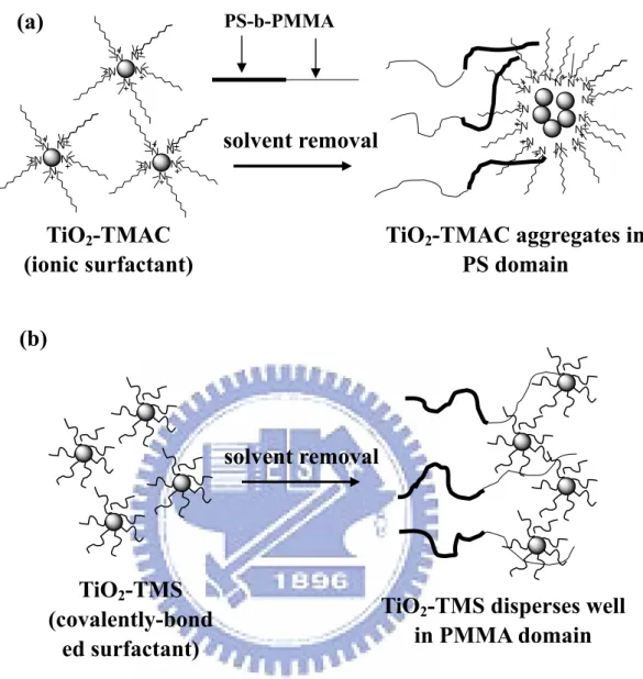
Block copolymers have been utilized not only as surfactants to inhibit coalescence and aid in the dispersion of nanoscale particles (e.g., metals, metal oxides, inorganic nanostructures, molecular chromophores, and quantum dots) but also to spatially pattern them. Our group has previously reported[37] the formation (Figure 1-10) of ordered clusters of surfactant-modified TiO2 nanoparticles (NPs) in the
selective block of lamellar assemblies of the diblock copolymer poly(styrene-b-methyl methacrylate) (PS-b-PMMA). Instead of using a water or alcohol phase, TiCl4 or titanium tetraisopropoxide precursors were used to synthesize
the TiO2 NPs in tetrahydrofuran, which is a good solvent for block copolymers.
amphiphilic surfactants were used to modify the TiO2 NPs. This process provides a
new approach toward the selective dispersal of quantum-confined NP clusters in a PS-b-PMMA diblock copolymer exhibiting an ordered lamellar phase. 3D and 2D nanostructure of CdS clusters have been prepared in the bulk and as thin films, respectively, by selectively dispersing pre-synthesized CdS NPs, containing hydroxyl groups on their surfaces, in the PEO block of templating poly(styrene-b-ethylene oxide) (PS-b-PEO) diblock copolymers.[38–42] Russell et al. reported that mixtures of diblock copolymers and either cadmium selenide- or ferritin-based NPs exhibit cooperative, coupled self-assembly on the nanoscale.[43] In thin films, the copolymers assemble into cylindrical domains, which dictate the spatial distribution of the NPs; segregation of the particles to the interfaces mediates interfacial interactions and orients the copolymer domains normal to the surface, even when one of the blocks is strongly attracted to the substrate. Figure 1-11 presents a cross-sectional TEM image of 100% PS thiol-coated Au NPs dispersed on a symmetric poly(styrene-b-2-vinylpyridine) (PS-b-P2VP) block copolymer. [44] We observe that the PS-coated Au NPs were located near the center of the PS block phase of the lamellar structure, whereas P2VP-coated Au NPs were located in the P2VP domain, as expected. Particles coated with a homopolymer similar to one of those in the copolymer can result in lower enthalpy when segregating into the corresponding domain of the block copolymer. Positioning the particle near the center of the corresponding polymer domain leads to better embedding of the NP because the polymer chains can accommodate particles by moving apart, rather than by stretching. Particles coated with a mixture of PS and P2VP thiols become localized exactly at the interface between the PS and P2VP block phases (Figure 1-11b).
1-1-3-3 Nanoreactors for Nanostructure Production
inorganic NPs. Reviews of the subject are available.[45,46] Two basic approaches have been developed. The first involves the binding of inorganic species to the monomer prior to polymerization or to one of the blocks of the copolymer prior to micellization (which may be induced by the ion binding event).[45] The second, more-important approach, however, involves the loading of preformed micelles, whether in solution or in bulk.
Bronstein and coworkers employed various types of block copolymers to prepare micellar nanoreactors for the fabrication of metallic NPs. In many cases, they took advantage of the fact that the N atoms of poly(vinylpyridine), P2VP, and P4VP allow their copolymers to form complexes with metal salts.[47,48] For example, they produced palladium clusters through the reduction of Pd(CH3COO)2 coordinated to
the P4VP micellar cores formed from poly(styrene-b-4-vinylpyridine) (PS-b-P4VP) diblocks in toluene.[47,49] Other metal nanoclusters, including cobalt,[50] Au,[47–49] rhodium,[47] and platinum,[47] have been prepared in a similar manner. The catalytic hydrogenation properties of these nanoclusters havebeen evaluated.[47,49] TiO2 NPs
have several interesting applications in such areas as catalysis, water purification, and UV blocking. In a previous study, our group synthesized arrayed needle-like TiO2
nanostructures using a PS-b-P4VP diblock copolymer as the template.[51] These nanostructures, which exhibited the rutile phase of crystalline TiO2, were grown on a
Si substrate presenting TiO2 seeds prepared using a thin layer of PS-b-P4VP. This
approach allowed the needle-like rutile TiO2 nanostructures to be fabricated with
variable spatial locations and densities. For example, the distance between two TiO2
needle bunches could be controlled from 120 to 160 nm when using block copolymer templates of different molecular weights (Figure 1-12).
Photonic crystals are attracting a huge amount of attention because they can be used to control and confine light. Materials with a complete bandgap reflect light (incident from any direction) within the wavelength range of the gap. Block copolymers are interesting materials with which to construct photonic crystals because they can self-assemble into periodic structures in one, two, and three dimensions. The inherently low dielectric contrast between the polymeric domains can be overcome through selective doping and/or removal of one component.
Theoretical predictions have revealed the possibility of photonic bandgaps existing in single- and double-network bicontinuous cubic structures.[52] These calculations have indicated, however, that (for the parameter space explored) no complete bandgaps exist for bicontinuous double primitive, double gyroid (body-centered cubic), or double diamond (face-centered cubic) structures. Bandgaps are anticipated for the single-network analogues, with the best candidate being single-diamond structures exhibiting dielectric contrast as low as 3.6. The optical reflectivity characteristics of an experimentally realized large-domain double-gyroid structure have been assessed.[40] The initial material selected was a PS-b-PI diblock of high molar mass, leading to a cubic lattice parameter a of 258 nm. The optical properties were measured for a bulk film and for a sample in which the PI block was removed through UV/ozone treatment (Figure 1-13), creating an interpenetrating PS network structure. As anticipated theoretically, a complete bandgap was not observed, although a wavelength range with high reflectivity was identified. This range shifted to lower wavelength in the etched structure.
1-2 Nanoparticles
Colloidal nanocrystals are sometimes referred to as “artificial atoms” because the density of their electronic states—which controls many of their physical
properties—can be widely and easily tuned by adjusting the crystal’s composition, size, and shape. The combination of size- and shape-dependent physical properties and ease of fabrication and processing makes nanocrystals promising building blocks for materials possessing designed functions.[53,54] The ability to control the uniformity of the size, shape, composition, crystal structure, and surface properties of nanocrystals is not only of technological interest: access to defined nanoscale structures is essential to uncovering their intrinsic properties, unaffected by sample heterogeneity. A rigorous understanding of the properties of individual nanocrystals will enable us to exploit them, making it possible to design and build novel electronic, magnetic, and photonic devices—and other functional materials based on these nanostructures.
1-2-1 Semiconductor Nanoparticles
Semiconductor NPs possess inorganic cores that are stabilized by a layer of surface surfactants. NPs featuring semiconductors as the inorganic material—so-called quantum dots—exhibit size-tunable band gaps. Quantum dots exhibit two deining characteristics: the surface area effect and the quantum confinement effect. The surface area effect exist for particles in a small size regime, where a large percentage of the atoms are located on or near the surface; for example, 99% of the atoms are positioned on the surface for a 1-nm-sized particle. [55] Such a vast interface between the NPs and the surrounding medium can have a profound effect on the particles’ properties; for example, the imperfect surface of the NPs may act as electron and/or hole traps upon optical excitation. Thus, the presence of these trapped electrons and holes can, in turn, modify the optical properties of the particles. In the quantum confinement effect, “confinement” and “quantization” have two closely related definitions: if a particle is “confined,” then its energy is “quantized,” and vice versa. According to the dictionary, to “confine” mean to “restrict within
limits” to “enclose”, and even to “imprison”. Quantum confinement not only causes an increase in the energy gap (a blue shift of the absorption edge) and splitting of the electronic states but also changes the densities of state and the exciton oscillator strength.[56] Many of the differences that exist in the electronic behavior of bulk and quantum-confined low-dimensional semiconductors are due to differences in their densities of state.
1-2-1-1 CdSe Nanoparticles
In 1993, Murray, Norris, and Bawendi described the preparation of nearly monodisperse CdS, CdSe, and CdTe semiconductor NPs.[57] CdSe NPs are potential building blocks for new electronic and optical nanodevices, such as light-emitting diodes, solar cells, lasers, and biological labels.
1-2-2 Metal Nanoparticles
Physicists predicted that metal NPs in the diameter range 1–10 nm (intermediate between the sizes of small molecules and bulk metals) would display electronic structures that reflect their electronic band structures, owing to quantum-mechanical rules.[58] The resulting physical properties are those of neither the bulk metal nor molecular compounds; instead, they depend strongly on the NP’s size, shape, interparticle distance, and nature of the protecting organic shell.[59] The few “last metallic electrons” are used for tunneling processes between neighboring particles—an effect that can be detected through impedance measurements that distinguish intra- and intermolecular processes.
1-2-2-1 Au Nanoparticles
Au NPs are the most stable metal NPs. They are fascinating materials for applications in several fields; for example, materials science (because of their multiple modes of assembly), physics [because of the behavior of individual particles and their size-related electronic, magnetic, and optical properties (quantum size effect)],
catalysis, and biology. The bottom-up approach exploited in nanotechnology is making them key materials and building blocks for the 21st century.
As mentioned above, the few “last metallic electrons” of Au NPs are used for tunneling processes between neighboring particles. The quantum size effect is involved when the de Broglie wavelength of the valence electrons is of the same order as the size of the particle itself. In such a system, the particles function electronically as zero-dimensional quantum dots (or quantum boxes) that behave according to quantum-mechanical rules. Freely mobile electrons are trapped in such metal boxes and display a characteristic collective oscillation frequency of the plasma resonance, giving rise to the so-called plasmon resonance band (PRB) observed near 530 nm in the 5–20-nm-diameter range. Au NPs are potential building blocks for memory cells,[60] single-electron transistors,[61,62] biological sensors,[63] and catalysts.[64]
1-3 Block Copolymer/Nanoparticle Mixtures
Diblock copolymer/NP nanocomposites have attracted much attention because the microphase separation of the copolymer can direct the spatial distribution of NPs
and, thereby, tailor the properties of the composite. In recent years the preparation
of various types of block copolymer/NP composite materials has progressed dramatically, placing the polymer–NP interface in the limelight of assembly processes.[65–68] Composite structures on the nanometer length scale promise to be candidates for next-generation materials, with many applications expected for nanocomposite-based devices.[69] An important aspect of this endeavor is the incorporation of non-polymeric properties into a polymeric matrix; this process can be achieved only as a result of the unique properties of nanoparticulate structures. Understanding the basic principles determining the optical, electronic, and magnetic
properties of the resulting composites will allow the construction of ordered arrays of NPs within polymer matrices to become an important means of tuning the properties of nanocomposites.
1-3-1 Controlled Arrangement of NP Arrays in Block Copolymer Domains
Nanoscience is at present searching for simple methods to arrange nanosized objects by means of bottom-up processes. Self-assembly processes are the method of choice to achieve this goal, focusing on the tailoring of supramolecular and interfacial forces and interactions. Thus, nanostructured diblock copolymer open up new avenues for fabricating ordered NP arrays using simple solution procedures. 1-3-1-1 Theory and Simulation
Theoretical and computer simulation investigations of NP–polymer composites have revealed the detailed mechanisms responsible for the development of their structures and physical properties. Huh et al. performed lattice Monte Carlo simulations to examine the phase behavior of NPs in melted-block copolymer domains.[70] Thompson et al.studied A–B block copolymer–NP composites using a combination of self-consistent field theory (SCFT) for the block copolymer and density functional theory (DFT) for the NPs (Figure 1-14).[71] To simplify the effect between the block chains and the NPs, they set the enthalpic interaction Flory–Huggins parameter of a particle P to a value of χAP of 0, thereby treating the
particles as identical to the A-block phase (enthalpic interaction Flory–Huggins parameter χAP = 0) and repelling it by the B-block phase (χBP = χAB = χBA), causing the
particles to localize preferentially in the A domains. They found that larger NPs were located at the center of the preferred copolymer domain; smaller NPs were driven nearer to the A–B interface as a result of the domination of the translational energy of the NPs in relation to the reduced chain stretching of the A chains. The specific morphology of the nanocomposite depended not only on the block
copolymer’s architecture but also on parameters such as the size and volume fraction of the particles. Diblock copolymer melts in the lamellar phase featuring spherical NPs that have an affinity for one particular block were predicted to have lower tensile moduli than those of the corresponding pure diblock-copolymer systems[72] because of swelling of the lamellar domain by the NPs and the displacement of macromolecules by the elastic inert fillers (NPs). Lee et al. used SCFT to study nanocomposites confined between walls, concluding that perpendicular or parallel orientations of the lamellae were preferred depending on the NP concentration and size and the strength of their interactions with the copolymers or walls.[73] Schultz et al. performed discontinuous molecular dynamics (DMD) simulations of block copolymer–NP composites,[74] revealing that NPs that do not interact with either blocks A or B tend to localize at the A–B interface, whereas NPs that repel block A tend to localize in domain B. The specificity of the localization increased with the NP size for neutral and strongly interacting NPs, but decreased for moderately interacting NPs. Small NPs have the largest effect on the periodic spacing, increasing the periodic spacing as a function of NP interaction strength. In general, the effect of the NPs on the periodic spacing decreases as the size of the NPs increases.
1-3-1-2 Methods to Control the Spatial Distribution of NPs in a Block Copolymer 1-3-1-2-1 In Situ Method
Metal NPs can be incorporated into the block copolymer domain by using in situ preparation methods, i.e., reduction of metal ions in one of the block domains.[75] Sohn et al. fabricated a multilayered nanostructure of alternating pure polymeric lamellae and Au NP-containing lamellae by using thin films of symmetric PS-b-P4VP and in situ preparation at room temperature.[76] First, multilayers of lamellae aligned parallel to the substrate were prepared on silicon wafers or mica substrates. After annealing, the thin films of PS-b-P4VP were immersed into ethanol solutions of
HAuCl4. The thin films loaded with HAuCl4 were then dipped into a NaBH4
solution to reduce the precursors to Au NPs selectively in the parallel lamellae of the P4VP block.[77] In this process, tetrachloroaurate ions [AuCl4]- (from the gold
precursor) become coordinated to the pyridine units of the P4VP block by protonation and, thus, are located selectively in the P4VP layers. The loaded precursors are the reduced by the aqueous NaBH4 solution to form Au NPs within the P4VP layers.
The precursors and reducing agents diffuse readily through each PS layer because ethanol and water can swell only the P4VP block.[78] Figure 1-15 displays a multilayered structure of alternating PS layers and Au NP-containing P4VP layers. 1-3-1-2-2 Ex Situ Method
One of the first composite materials containing metal NPs and diblock copolymers was reported by Hamdoun et al.[79] Maghemite (Fe2O3) was prepared
with desired features and then coated with a compound that could “dissolve” in a melt of one of the block phases but not in that of the other. A grafted short chain of polystyrene was used to cover the maghemite NPs to facilitate their dissolving in one part of the two blocks of a symmetric polystyrene-b-poly(butyl methacrylate) (PS-b-PBMA) lamellar structure. Indeed, a high concentration of NPs was distributed homogeneously within the PS microdomains. For semiconductor NPs, selective sequestration has been demonstrated for pre-synthesized surface-modified TiO2 and CdS NPs into single blocks of PS-b-PMMA[37] and PS-b-PEO,[38]
respectively. After the preparation of the NPs, the particle core size is the most significant parameter affecting the localization of particles along the interface between the two blocks or at the center of the respective polymer domain. The self-assembly of two kinds of NPs simultaneously directed on a monolayer film of diblock copolymer micelles, reported by Sohn et al., was also considered with respect to the size of each particle.[80] Dodecanethiol-protected Au NPs (R = 5.4 nm)
immersed in PS-b-P4VP spherical micelles resulted in the Au NPs being decorated around the hexagonally ordered micelles; they were not, however, located in the entire PS corona because they were much smaller than the PS-b-P4VP micelles. When surface-modified Au NPs were added to PS-b-P4VP micelles containing FeCl3 (R =
16 nm), the Au NPs surrounded the hexagonally ordered iron oxide NPs (Figure 1-16). Larger-sized iron oxide NPs were located in the centers of the P4VP domains; the ordering was preserved after plasma etching of the polymeric matrix.
1-3-1-2-3 Methods Using External Fields
UV-light irradiation has often been used to prepare templates or holes for NP arrangement. Exposure of a thin film of PS-b-PMMA to UV irradiation decomposes the PMMA phase and induces crosslinking of the PS phase, thereby producing an ideal template wherein NPs could be sequestered.[31,81] A spin-coated thin film of PS-b-PMMA that was exposed to UV light under vacuum and immersed in glacial acetic acid led to selective removal of the degraded PMMA phase from the PS matrix.[82] The resulting hexagonally ordered cylindrical pores acted as templates when dipped into a solution containing NPs, leading to the efficient sequestration of NPs into the pores. There are two parameters that are critical to the success of this procedure: the diameter of NPs should be smaller than that of the nanopores and the ligands stabilizing the NPs should not exert a strong affinity toward the PS matrix. Figure 1-17 presents the TEM image of a template featuring 17-nm-diameter pores filled with 10-nm-diameter CdSe NPs.
1-3-1-2-4 Directed Chemical-Binding Methods
The direct chemical binding of NPs onto block copolymer surfaces is also an important method in generating ordered particle arrays.[83,84] The critical points affecting the direct binding between NPs and block copolymers are (a) the chemical nature of the block copolymer domain to which the NPs will be bound, (b) the
chemical structure of the shell around the NPs, and (c) the interaction between the surface of the block copolymers and the NPs. The deposition of layered NPs on the polymer surface, mediated by covalent bonds, has been described; it relies mainly on supramolecular interactions[85] (e.g., the molecular printboards of Reinhoudt and co-workers),[86] hydrogen bonding systems,[87] and purely electrostatic assembly[65,88] at appropriately structured surfaces. In another approach, our group used strong hydrogen bonding interactions to bind Au NPs onto microphase-separated block copolymer films deposited on surfaces (Figure 1-18).[89] Au NPs (diameter: 5 nm) were coated with ligands featuring barbituric acid moieties. Block copolymers were prepared bearing the matching receptor (i.e., the so-called Hamilton receptor) in one of the blocks and a fluorinated side chain in the other block to enhance the degree of microphase separation. The binding of Au NPs onto the block copolymer surface was mediated by the strong interactions existing between the barbituric acid and Hamilton receptor units.
1-3-2 Interests to Block Copolymer/NP Nanocomposites
1-3-2-1 NP-Induced Phase Transformation
In a previous study, our group reported the morphological transformation of a PS-b-P4VP diblock copolymer—from a hexagonally packed cylinder structure to a lamellar structure—that occurred upon sequestering CdS NPs in the P4VP block.[90] The surface of the CdS NPs was stabilized with mercaptoacetic acid as a surfactant, rendering each CdS NP hydrophilic. Whereas pure PS-b-P4VP possessed a hexagonally packed cylindrical structure, the composite transformed into a lamellar structure in the presence of 7 wt% of the CdS NPs (Figure 1-19). This morphological transformation, from a cylindrical to lamellar structure, was mediated by strong interaction forces, such as hydrogen bonds, between the carboxylic acid units of the CdS NPs and the P4VP chains. Such an NP-induced phase
transformation was also reported by Kramer’s group; they used polymer-coated Au NPs to induce phase transformations that were affected by the choice of solvent or the depth of the bulk film.[91]
1-3-2-2 Interfacial Interactions
Interfacial interactions significantly affect the spatial distribution of NPs within homopolymers and block copolymers and the global structure of the particle-filled systems. Bockstaller et al.[92] observed that the localization of particles along the interface or at the center of the respective polymer domains was also affected by the particles’ core sizes. In a system consisting of symmetric polystyrene-b-ethylene propylene (PS-b-PEP), large silica NPs (d = 21.5 nm; d/L = ca. 0.26; d: particle diameter; L: respective domain dimension of the block copolymer) were located at the center of the PEP domain. Smaller Au NPs (d = 3.5 nm; d/L = ca. 0.06) segregated at the interface between two block phases (Figure 1-20) in accordance with theoretical simulations.[71] Interfacial segregation of NPs is expected to occur for particle sizes at which d/L is less than 0.2; localization of NPs at the center of the lamellar phase is expected for values of d/L that are greater than 0.3.
1-3-2-3 Proximity Effects in Block Copolymer/NP Composites
Dependent on the surface chemistry of Au nanocrystals of equal metal core size, two morphological types of self-organized block copolymer–particle blends are observed (Figure 1-21):[93] (1) segregation of nanocrystals to the interfacial areas and (2) preferential uniform distribution within one of the respective polymer domains. Confinement of the nanocrystals to the narrow interfacial regions of the microstructure in the first type of blend results in high local particle filling fractions and gives rise to electromagnetic coupling upon light irradiation, accompanied by a pronounced increase in absorbance.
In a previous study, our group reported the collective electron transport behavior of Au NPs confined within a single P4VP nanodomain and within homo-P4VP.[94] Figure 1-22 displays representative current–voltage scaling data obtained for these two samples at 78 K. The accessible current-conducting pathways are described[95–99] by Eq. (1-5): ζ ⎟ ⎠ ⎞ ⎜ ⎝ ⎛ − ∝ 1 T V V I (1-5)
(for V > VT ), where I is the current, V is the voltage, ζ is a scaling exponent, and
T
V is the threshold voltage. The scaling exponent ζ can be regarded as the ensionality for collective electron transport fo f dots, as modeled in a previous study.[99] We obtained power-law scalings (
dim r arrays o
ζ ) of 1.31 for the nanodomain-confined sample and 2.84 for the randomly distributed sample. These results indicate that quasi-one-dimensional collective electron transport occurs for the nanodomain-confined Au NPs and that quasi-three-dimensional collective electron transport occurs for the randomly distributed Au NPs.
1-3-2-5 Memory Device Applications
Leong et al. demonstrated the versatility of combining self-assembled block copolymers with in situ room-temperature synthesis of Au NPs in the copolymer matrix as an effective approach toward polymer memory fabrication (Figure 1-23).[100] Their proof-of-concept experiment revealed the vast potential of these fascinating nanoscaled arrays of NPs. Moreover, they demonstrated the ability to tune the memory behavior by controlling the loading of Au NPs. A memory structure featuring pentacene as the organic semiconductor exhibited a clockwise C–V hysteresis, indicating a net hole trapping effect. This novel structure displayed a large memory window of 2.1 V after writing and erasing modes and a long charge retention ability of ca. 92% over 60,000 s. This approach, by virtue of its simplicity
in design and processing, can realize integrated memory devices and circuits for low-cost plastic electronics applications.
1-4 Organic Electrical Bistable Memory Device
Organic materials have attracted much attention for the construction of large-area, mechanically flexible electronic devices.[101] Organic light-emitting diodes for flat-panel displays are ready for mass production,[102] and significant progress has also been made in organic thin-film transistors[103] and organic solar cells.[104] There is a strong desire to develop new advanced materials that can overcome the potentially limiting scaling difficulties present in the semiconductor industry. Development of future information technology could come from data storage incorporating these advanced materials. Many methods have been reported for achieving inorganic nonvolatile memory, such as implementing phase-change memory,[105] programmable metallization cells,[106] mechanical switches,[107] quantized atomic switches,[108] quantum dots,[109] and nanocrystal memory.[110] Organic materials are promising candidates for electronic devices in new information technologies.[111] The devices can be fabricated either through bottom-up methods or by forming composite active layers; they can easily be addressed by x–y cross-wires, i.e., two-terminal structures that sandwich the active layer. The use of organic materials provides a simplified manufacturing process yielding low-cost, flexible, light-weight devices that have an active device area approaching the nanoscale.
1-4-1 Typical I–V Behavior of an Organic Memory Device Organic
In general, the memory effect observed in these organic devices is related to charge storage (including charge trapping, charge separation, and change transfer) within active components in the organic layer.[112,113] The critical material requirement for the memory effect is the existence of an energy barrier preventing the