I
國立交通大學
材料科學與工程研究所
碩士論文
以超高真空化學氣相沉積系統成長鍺磊晶層
於磷化銦鎵/砷化鎵基板之研究
Epitaxial Growth of Germanium on In
0.5Ga
0.5P/GaAs substrates
by UHVCVD
研究生:關景文
指導教授:張 翼 博士
II
以超高真空化學氣相沉積系統成長鍺磊晶層
於磷化銦鎵/砷化鎵基板之研究
Epitaxial Growth of Germanium on In
0.5Ga
0.5P/GaAs substrates
by UHVCVD
研究生:關景文
Student: Ching Wen Kuan
指導教授:張 翼 博士
Advisor: Dr. Edward Yi Chang
國立交通大學
材料科學與工程研究所
碩士論文
A Dissertation
Submitted to Department of Materials Science and Engineering
National Chiao Tung University
In Partial Fulfillment of the Requirements
For the Degree of Master in
Material Science and Engineering
2014
Hsinchu, Taiwan, Republic of China
中華民國 103 年十一月
III 以超高真空化學氣相沉積系統成長鍺磊晶層於磷化銦鎵/砷化鎵基板之研究 研究生:關景文 指導教授:張 翼 博士 國立交通大學材料科學與工程研究所 摘要 為了解決矽半導體元件在線寬持續縮小的趨勢下所遇到的問題,以鍺磊晶薄 膜作為通道材料因應其高電動遷移率(1900 cm2/V-s)的特性被視為一種可行的解決方 案。本篇論文首度利用超高真空化學氣相沉積系統(UHVCVD)成長鍺磊晶層於磷化銦 鎵/砷化鎵基板,並對於此結構的特性與成長機制做進一步的探討。 透過表面化學電子能譜儀(XPS)分辨出表面元素覆蓋率不同之磷化銦鎵上成長鍺 磊晶層的誘導期(incubation time)有所不同,這是由於鍺原子與銦原子及鎵原子之鍵結 能差異所致。根據熱毛細力理論(thermodynamic theory of capillarity)的計算,鍺磊晶層 成長於磷化銦鎵/砷化鎵基板的模式為 3D 成長(Volmer-Weber growth mode);利用掃描 式電子顯微鏡(SEM)和穿透式電子顯微鏡(TEM)的成像能夠進一步驗證此成長機制。 透過高解析度穿透式電子顯微鏡(HR-TEM)可以證明此論文中成長的鍺磊晶層擁有非 常好的結晶品質以及極低的缺陷密度;而光微區分析(EDS)的結果也顯示鍺和磷化銦 鎵之間的接面處只有極少的相互擴散(interdiffusion)產生。在螢光光譜(PL)的分析中可 發現鍺磊晶層直接能隙(0.8 eV)的放射光譜,由此亦可間接證明成長出來的鍺金屬有非 常好的品質。 從本論文結果可得知鍺和磷化銦鎵及砷化鎵的異質接面結構可應用於 p 型金氧半 場效電晶體(MOSFET),甚至可與 n 型三五族快速電子遷移率電晶體互相整合以利於 之後 CMOS 元件的發展。
IV
Epitaxial Growth of Germanium on In0.5Ga0.5P/GaAs substrates by UHVCVD
Student: Ching Wen Kuan Advisor: Dr. Edward Yi Chang Department of Material Science and Engineering
National Chiao Tung University
Abstract
Epitaxial Ge film for channel material is regarded as the solution to the problems of the limitations of silicon-based device performance as continuing reducing the feature size because of its high hole mobility (1900 cm2/V-s). Ge epitaxial film was firstly grown on
In0.5Ga0.5P/GaAs (100) with 6°-offcut toward [110] substrates by ultra-high vacuum chemical
vapor deposition (UHVCVD). The structure was designed for the fabrication of p-channel MOSFET, and thus the p-channel MOSFET can be useful for beyond-the-CMOS-roadmap logic applications. The incubation time was found to be associated with the surface
composition ratio of InGaP characterized by X-ray photoelectron spectroscopy (XPS). The growth mode of epitaxial Ge grown on In0.5Ga0.5P/GaAs (100) is the Volmer-Weber growth,
calculated by the thermodynamic theory of capillarity and the pattern was further
characterized by transmission electron microscopy (TEM) and scanning electron microscopy (SEM). Good single crystal quality and low defect density of Ge films were observed
according to high-resolution TEM images. Minimal interdiffusion and sharp interface between Ge and InGaP was demonstrated by energy-dispersive X-ray spectroscopy (EDS) line scan profile of TEM. Direct band gap emission at 0.8 eV of Ge epitaxial film was detected by photoluminescence (PL) spectrum.
V
Acknowledgement
I would like to express my special appreciation and thanks to my advisor Professor Edward Yi Chang, your advice on both research as well as on my career have been priceless. I would also like to express my gratitude to my supervisor Maggie Su for introducing me to the topic as well for the support on the way. Furthermore I would like to thank Chi Lang Nguyen for the useful comments, remarks and engagement through the learning process of this master thesis. Also, I like to thank the participants in my survey, who have willingly shared their precious time during the process of interviewing. I would like to thank my loved ones, who have supported me throughout entire process, both by keeping me harmonious and helping me putting pieces together. I will be grateful forever for your love.
VI
Contents
Abstract (Chinese)…...………. III Abstract (English).……….………. IV Acknowledgement……….. V Contents………... VI Table Captions………...…………. VIII Figure Captions……….. IX
Chapter 1 Introduction
1.1 Background and Motivation………... 1
1.2 Material Growth of Ge on InGaP/GaAs Substrate………. 1
1.3 Outline of the Dissertation………. 2
Tables……… 3
Figures……….. 4
Chapter 2 Literature Review: Characterization of the InxGa1-xP–GaAs System 2.1 III-V Ternary alloys……….... 6
2.2 InxGa1-xP/GaAs system……….. 7
2.2.1 Introduction……….. 7
2.2.2 Growth Details………. 7
2.2.3 Microstructure properties………. 9
2.3 Single crystal Ge film on InxGa1-xP………... 10
Tables……… 11
VII
Chapter 3 Ultra High Vacuum Chemical Vapor Deposition (UHVCVD) System, Experimental Procedure and Characterization Methods
3.1 Chemical vapor deposition (CVD) system………. 16
3.1.1 Ultra high vacuum CVD (UHV/CVD) system………. 17
3.1.2 Chemical reaction in UHV/CVD……….. 18
3.2 Ge film epitaxy in UHV/CVD……… 19
3.3 Fundamental of characterization techniques……….. 20
3.3.1 Scanning electron microscopy (SEM)……….. 20
3.3.2 Transmission electron microscopy (TEM)………... 23
3.3.3 Atomic force microscopy (AFM)………. 25
3.3.4 Photoluminescence spectroscopy (PL)………. 27
3.3.5 X-ray electron spectroscopy (XPS)……….. 28
Figures……….. 31
Chapter 4 Results and Discussion 4.1 Incubation Time and Growth Rate………. 37
4.2 Growth Mode of Ge on In0.5Ga0.5P (100)………... 38 4.3 Surface Roughness………. 39 4.4 Crystal Quality………..…. 40 4.5 Interdiffusion……….……. 40 4.6 Photoluminescence………. 41 Figures……….. 42 Chapter 5 Conclusions……….. 49 Reference……… 50
VIII
Table Captions
Table 1.1 Material properties of popular semiconductors……… 3
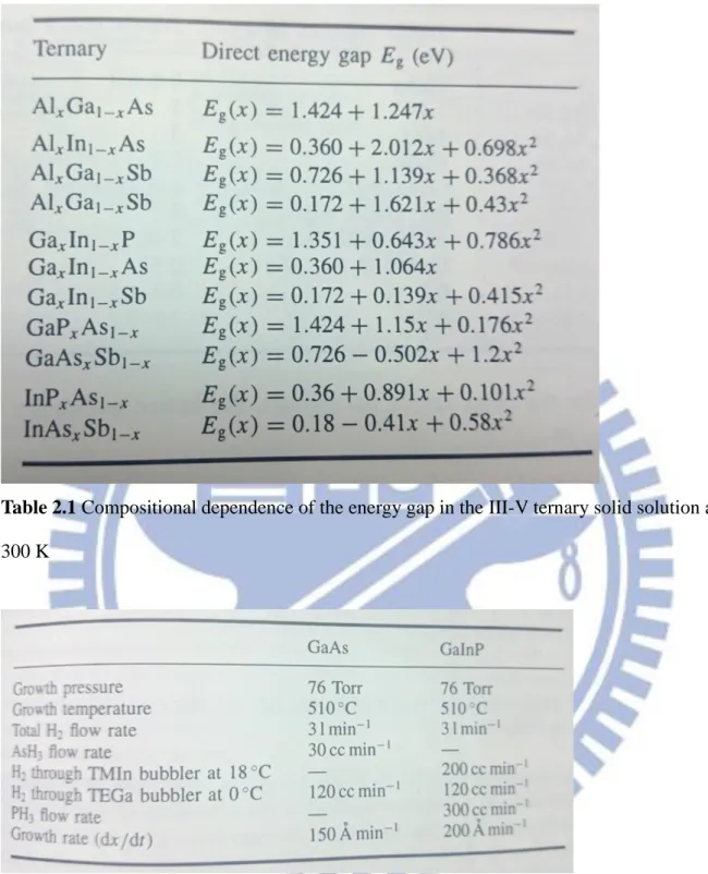
Table 1.2 Material properties of In1-xGaxP, Ge and GaAs at 300 K…………. 3 Table 2.1 Compositional dependence of the energy gap in the III-V ternary solid
solution at 300 K………... 11
IX
Figure Captions
Figure 1.1 The comparisons of lattice constant and energy band gap between semiconductor
materials……….. 4
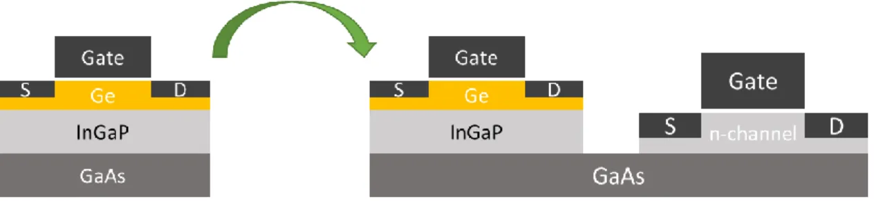
Figure 1.2 The prospects of p-channel MOSFET can be integrated with n-channel III-V material devices on the same GaAs template for complimentary architecture for beyond-the-CMOS-roadmap logic applications……….. 5
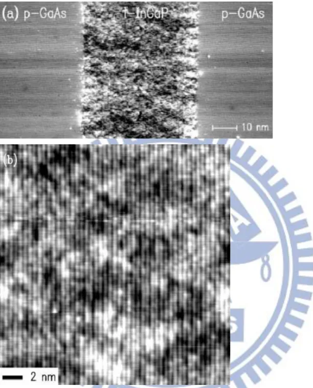
Figure 2.1 (a) STM image of p-GaAs/i-InGaP/p-GaAs heterostructure, acquired with sample voltage of 2.5 V. (b) High-resolution image of InGaP layer, acquired with sample voltage of – 2.0 V and displayed with a gray scale of 0.5Å . Growth direction is from right to left……….………… 12
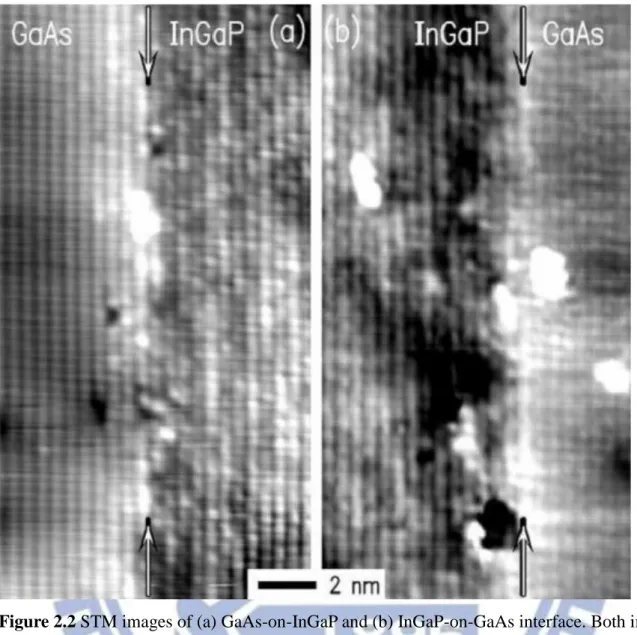
Figure 2.2 STM images of (a) GaAs-on-InGaP and (b) InGaP-on-GaAs interface. Both image were acquired with sample voltage of –2.0 V and are displayed with gray scales of 0.9 Å . Growth direction is from right to left……….. 13
Figure 2.3 Experimental rocking curves of 600Å Ge layer on InxGa1-xP /GaAs………..………. 14
Figure 2.4 Ge film deposited on InxGa1-xP/GaAs (100) from the sample as shown in Figure 2.3 Epitaxial Ge with a smooth InGaP interface is observed in lattice fringes……….. 15
Figure 3.1 A typical scheme of a CVD reactor………..…. 31
Figure 3.2 Schematic of UHVCVD system……….... 31
Figure 3.3 Plot of the excitation volume generated by the SEM electron beam………... 32
Figure 3.4 A schematic of transmission electron microscope………... 32
Figure 3.5 A schematic of atomic force microscopy………..……. 33
X
Figure 3.7 Schematic band diagrams for the photoluminescence processes... 34
Figure 3.8 Schematic of an emission experiment of PL measurement………... 34
Figure 3.9 Surface irradiated by sufficient energy X-ray photon beam will emit
photoelectrons: phenomenon (left) and principle schematic (right)………. 35
Figure 3.10 (a) The X-ray photon transfers its energy to a core-level electron leading to
photoemission from the n-electron initial state. (b) The atom, now in an (n-1)-electron state, can reorganize by dropping an electron from a higher energy level to the vacant core hole. (c) Since the electron in (b) dropped to a lower energy state, the atom can rid itself of excess energy by ejecting an electron from a higher energy level. This ejected electron is referred to as an Auger electron. The atom can also shed energy by emitting an X-ray photon, a process called X-ray fluorescence………. 35
Figure 3.11 Schematic design of an X-ray photoelectron spectrometer………... 36
Figure 4.1 (top) Plot of Ge film thickness versus growth time on different surface coverage
InGaP layers. The incubation time are 29.4 and 38.9 minutes for indium coverage of 27.82% and 45.84%, respectively. (bottom) The analysis of composition ratio on InGaP surfaces revealed by XPS……… 42
Figure 4.2 Plot of Ge film thickness versus growth time with GeH4 gas flow rate of 10 and 20
sccm, respectively, during growth……… 43
Figure 4.3 An illustration of the basic processes of vapor deposition on a surface of a
substrate………..…….. 43
Figure 4.4 Top view surface morphology of Ge grown on In0.5Ga0.5P/GaAs characterized by
SEM at growth time of (a) 20, (b) 38, and (c) 45 minutes……….... 44
Figure 4.5 Cross-sectional view surface morphology of Ge grown on In0.5Ga0.5P/GaAs
characterized by TEM at thickness of (a) 40, and (b) 190
XI
Figure 4.6 Plot of surface roughness and film thickness of Ge versus growth
time……… 46
Figure 4.7 Plot of surface roughness of Ge versus growth time in different growth
conditions……….. 46
Figure 4.8 Cross-sectional high-resolution TEM image and diffraction pattern of 190 nm Ge
epitaxial layer………...…………. 47
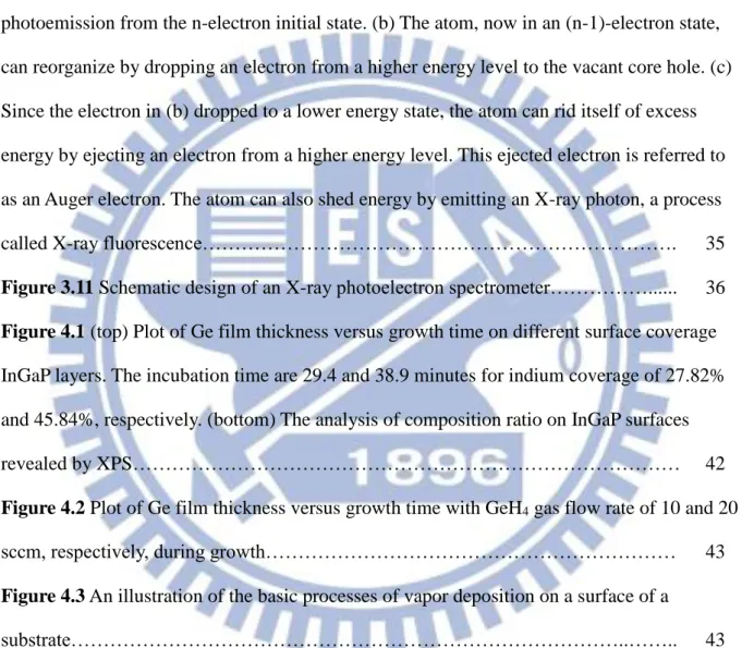
Figure 4.9 High-resolution TEM microstructure and the EDS line scan profile across two
interfaces of Ge/In0.5Ga0.5P/GaAs structure………...……… 47 Figure 4.10 Room temperature photoluminescence infrared emission from the structure of 1.8
μm Ge film on In0.5Ga0.5P/GaAs substrate. The direct band gap emission occurs at 0.8
1
Chapter 1
Introduction
1.1 Background and MotivationIn the past several decades, there has been a steady step-up of device performance along with the continued reduction of device feature sizes for silicon devices. With continued transistor scaling, new materials and device architectures are being introduce at a rapid pace to sustain an aggressive operating voltage scaling roadmap in a persistent effort towards enhancing the energy efficiency of the transistors. Furthermore, for small feature size silicon devices, additional gaining in carrier mobility can be achieved by applying a strain to the channel material [1]. Recently, III-V material has attracted a lot of attention due to their higher carrier mobility compared to that of Si devices. In contrast to these Si devices, high-speed devices made from III-V materials are characterized with a high electron mobility but still suffer from low hole mobility. It is very critical to explore a novel channel material with higher hole mobility that would provide an energy-efficient nanoscale FET for future
complementary structures [2]. In Table 1.1, it is obvious Ge is a good candidate for p-channel material because of its high hole mobility (1900 cm2/V-s). Typically, the Ge-p-channel
devices are usually fabricated on bulk Ge substrate [3,4], however, for post CMOS
applications, the growth of Ge on InGaP is a possible solution for materials integration since InGaP material has high resistivity, thus reduce the parasitic effect of the Ge device. The main disadvantage is that germanium based oxides are not stable and rather soluble in water. But the inevitable shift to high-κ/metal gate has made Ge a serious option nevertheless.
1.2 Material Growth of Ge on InGaP/GaAs Substrate
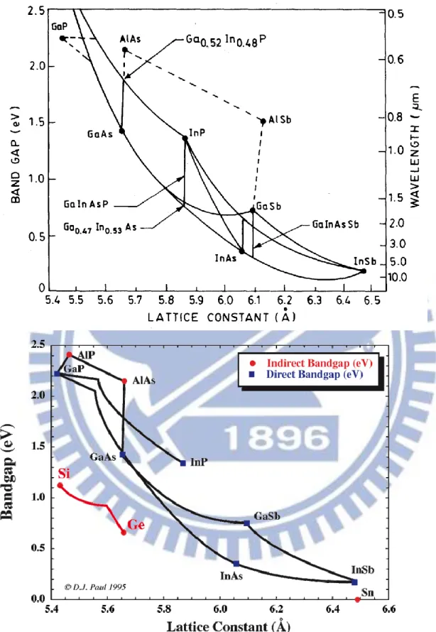
The Ge epitaxial growth on InGaP/GaAs or InGaP substrates has not been found to be discussed among the searchable literature. However, the Ge epitaxial film grown on GaAs is
2
of immense interest due to very low lattice mismatch (~0.08%) which ensures larger critical thickness and lower dislocation density (Figure 1.1) [5], and almost the same value of thermal expansion coefficients. Likewise, the Ge epitaxial growth on In0.5Ga0.5P holds the same
advantages mentioned above because of the close values of parameters such as lattice constant and thermal expansion coefficient in comparison with GaAs. Furthermore, the InGaP layer has a greater energy band gap than GaAs, resulting in a higher resistivity that provides with a better confinement of carriers in Ge. (Table 1.2)
Due to above reasons, the Ge epitaxial growth on InGaP/GaAs is discussed in this study for the first time. The growth mode of Ge on InGaP/GaAs and surface morphology as well as the crystal quality of Ge will be discussed in detail for the initial step forward to the
fabrication of p-channel MOSFET, and thus the p-channel MOSFET can be integrated with n-channel III-V material devices on the same GaAs template for complimentary architecture for beyond-the-CMOS-roadmap logic applications. (Figure 1.2)
1.3 Outline of the Dissertation
This dissertation covers the study of the surface properties and the crystal quality of Ge epitaxial film grown on InGaP/GaAs substrates. In chapter 2, the characterization of the In 1-xGaxP/GaAs system according to the literature is introduced. In chapter 3, the UHVCVD
system and experimental procedure in the study are demonstrated. Then, various analytic equipment to characterize the material quality and device performance of Ge/InGaP/GaAs structures would be presented.
In chapter 4, the experiment results are shown and discussed. High quality epitaxial Ge were grown on InGaP/GaAs substrates by ultra-high vacuum chemical vapor deposition (UHVCVD). The discussion about the incubation time and growth rate, growth mode, surface morphology, crystal quality, and interdiffusion will be presented here. Finally, the conclusions will be in the chapter 5.
3
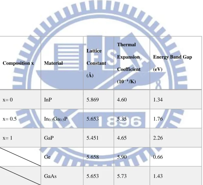
Table 1.1 Material properties of popular semiconductors
Composition x Material Lattice Constant (Å ) Thermal Expansion Coefficient (10⁻⁶/K)
Energy Band Gap (eV) x= 0 InP 5.869 4.60 1.34 x= 0.5 In0.5Ga0.5P 5.653 5.35 1.76 x= 1 GaP 5.451 4.65 2.26 Ge 5.658 5.90 0.66 GaAs 5.653 5.73 1.43
4
Figure 1.1 The comparisons of lattice constant and energy band gap between semiconductor
5
Figure 1.2 The prospects of p-channel MOSFET can be integrated with n-channel III-V
material devices on the same GaAs template for complimentary architecture for beyond-the-CMOS-roadmap logic applications.
6
Chapter 2
Literature Review: Characterization of the In
xGa
1-xP – GaAs System
2.1 III-V Ternary alloys [6]
When more than one element from group III or group V is distributed randomly on group III or group V lattices sites, III-III-V or III-V-V ternary alloys can be achieved. The notation most frequently used is IIIxIII1-xV or IIIVyV1-y. There are 18 possible ternary system among
the group III and group V elements of interest.
The bandgap energy Eg(x) of a ternary compound varies with the composition x as
follows:
Eg(x) = Eg(0) +bx +cx2 (2-1)
where Eg(0) is the bandgap energy of the lower binary compound and c is the bowing
parameter. The bowing parameter c can be theoretically determined (Van Vechten and Bergstresser 1970). It is especially helpful to estimate c when experimental data are
unavailable. The lattice constant of ternary compounds can be calculated using Vegard’s law. According to Vegard’s law the lattice constant of the ternary alloys can be expressed as follows:
Aalloy = xaA + (1-x)aB (2-2)
where aA and aB are the lattice constant of the binary alloys A and B. Vegard’s law is obeyed
quite well in the most of the III-V ternary alloys. The compositional dependence of the energy gaps of carious III-V ternary alloys at 300K is given in Table 2.1 (Casey and Panish 1978).
7 2.2 InxGa1-xP/GaAs system [6]
2.2.1 Introduction
In the past few years, AlxGa1-xAs /GaAs heterostructure have emerged as a promising
system for optoelectronics and microwave device applications. However, because of the strong reaction between Al and oxygen, even trace quantities of oxygen have a dramatic effect on the quality of AlxGa1-xAs layers due to the effective introduction of deep-level defects. One
of the solutions is to replace AlxGa1-xAs by InxGa1-xP/GaAs.
The electrical, optical and structural properties of InxGa1-xP/GaAs depend directly on
how the system is lattice matched. Concerning ΔEc, there is a surprise: if we assume that the
discontinuity in the conduction band is the difference in the electron affinities (χ) of χ(GaAs) = 4.05eV, χ(InP) = 4.4eV, χ(GaP) = 4.0eV (the electron affinity of InxGa1-xP is take as the
average of χ(InP) and χ(GaP) and χ(In0.49Ga0.51P) = 4.2eV), then ΔEc = χ(GaAs) – χ(InGaP) =
-0.15eV. However, the experiment results show that ΔEc = 0.2eV and ΔEv = 0.28eV.
The InxGa1-xP ternary alloy lattice matched to GaAs substrate has attracted a lot of
attention not only because it is a good alternative to AlxGa1-xAs /GaAs -based devices but also
because it is used as a model material to study the ordering effect and its influence on InxGa 1-xP properties.
2.2.2 Growth Details
InxGa1-xP layers can be grown by MOCVD, either at atmospheric pressure or low
pressure and at low temperatures between 500 and 6000C. One can use different group III
alkyls for Ga and In sources, and hydrides or alkyls for group-V P sources. Chemical reactions occurring among these sources are as follows:
0.51R3Ga + 0.49R’3In + EH3 H2
→ Ga0.51In0.49P +nCnH2n (2-3)
where R, R’ and E can be methyl, ethyl, alkyl or hydride.
8
triethylgallium (TEGa), trimethylindium (TMIn) and pure phosphine (PH3) in H2 carrier gas.
The optimum growth conditions are given in Table 2.2.
The growth rate (dx/dt) of InxGa1-xP depends on the flow rates of TMIn and TEGa
(group-III element) and is independent of PH3 flow rate (group-V element) and growth
temperature under the growth conditions listed in Table 2.2. The distribution coefficients of indium and gallium are defined as
K= 𝑋𝐺𝑎𝑆 / 𝑋𝐺𝑎𝑉 (2-4) and
K= 𝑋𝐺𝑎𝑆 / 𝑋𝐺𝑎𝑉 (2-5)
are nearly equal to unity. Figure 2.1 shows the variation of growth rate dx/dt of InxGa1-xP
lattice matched to GaAs with a growth temperature of TG= 5400C and growth pressure of 76
Torr. Similar results have been reported by Hsu et al (1985) at growth temperatures from 600 up to 6500C. They showed that there was no gas-phase reaction in their reactor leading to premature depletion of In or Ga.
An undoped InxGa1-xP layer grown under the conditions of table 2.2 has a free electron
carrier concentration of 5 x1014 cm-3 with mobility of 6000 cm2V-1s-1 at 300K and 40 000
9 2.2.3. Microstructure properties [7]
Compositionally abrupt InxGa1-xP /GaAs heterojunctions have been investigated by
cross-sectional scanning tunneling microscopy (STS) and spectroscopy. The advantage of such work is that band offsets can be measured while simultaneously imaging the atomic-scale structural properties of the interfaces. Images inside the InGaP layer reveal a random arrangement of In and Ga atom. This result is consistent with PL results and growth conditions for similar samples that indicate a nearly fully disordered InGaP layer [8]. It is found that GaAs-on-InGaP interface has a slightly wider transition region and more interface intermixing than the InGaP-on-GaAs interface. Both interfaces exhibit InGaAs-like
properties. Indium outdiffusion from InGaP into GaAs at the GaAs-on InGaP interface is clearly identified, although As/P interchange is not very obvious. Spatially resolved spectra reveal that nearly all of the band gap discontinuity occurs between the valence band edges.
In the large-scale STM image of Figure 2.1(a) the InGaP layer is seen in the center part of the image with GaAs layers seen on either side. Growth direction is from the right to the left for all images presented in this paper. The InGaP layer appears mottled due to
compositional fluctuations in the alloy. A high-resolution image of the InGaP layer is shown in Figure 2.1(b). At a sample bias of –2.0 V, filled states are imaged, i.e. localized on P atoms for InGaP. The pattern of different brightness for the P atoms reflects the distribution of neighboring In and Ga atoms. Because the cleaved surface is atomically flat, the observed contrast arises from a combination of electronic and strain effects, both associated with the presence in the alloy of clusters that are InP-rich or GaP-rich [9]. Ordering of the alloy is an important phenomenon for InGaP.
High-resolution images of inverted and normal InGaP/GaAs interfaces were shown in the Figure 2.2 (a) and (b), respectively. Atoms on the group V sublattice are imaged here, i.e. revealing As atoms in GaAs and P atoms in InGaP. Arrows indicate the nominal position of the interfaces. The two interfaces display different features. For the GaAs-on-InGaP interface,
10
the transition region is about 3-4 atomic bilayers (bilayer spacing is 5.65Å ) and most of it lies in the GaAs side. Some atom-size bright features are seen in the GaAs layer near the
interface. We attribute these features to In atoms. The image of In atoms will appear brighter because In atoms are bigger than Ga atoms (also the band gap of InAs is smaller than that of GaAs, which would contribute to a larger tunnel current near In atoms [9])
2.3. Single crystal Ge film on InxGa1-xP [10]
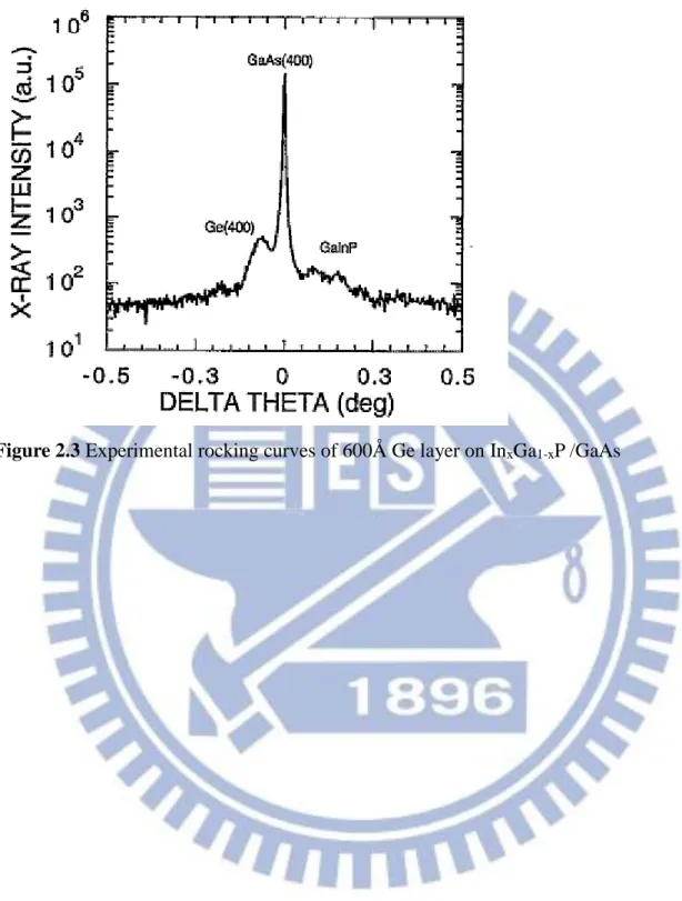
A 280 Å organometallic vapor phase epitaxy (OMVPE) InxGa1-xP film grown on (100)
GaAs. The film was slightly gallium rich so that its x-ray rocking curve could be discerned from the GaAs and the Ge, which has a lattice parameter slightly larger than that of GaAs. After that, 600Å Ge film was deposited on it at a rate of 0.3-0.5 Å /s.
The (400) GaAs rocking curve can be seen in Figure 2.3 for the GaAs/InxGa1-xP/Ge
structure along with the (400) InxGa1-xP and germanium rocking curves again suggesting that
the films grew epitaxially. This is verified in the TEM micro-graph in Figure 2.4 which also illustrates that both InxGa1-xP interfaces are relatively smooth. The germanium film grew
11
Table 2.1 Compositional dependence of the energy gap in the III-V ternary solid solution at
300 K
12
Figure 2.1 (a) STM image of p-GaAs/i-InGaP/p-GaAs heterostructure, acquired with sample
voltage of 2.5 V. (b) High-resolution image of InGaP layer, acquired with sample voltage of – 2.0 V and displayed with a gray scale of 0.5Å . Growth direction is from right to left.
13
Figure 2.2 STM images of (a) GaAs-on-InGaP and (b) InGaP-on-GaAs interface. Both image
were acquired with sample voltage of –2.0 V and are displayed with gray scales of 0.9 Å . Growth direction is from right to left.
14
15
Figure 2.4 Ge film deposited on InxGa1-xP/GaAs (100) from the sample as shown in Figure
16
Chapter 3
Ultra High Vacuum Chemical Vapor Deposition (UHVCVD) System,
Experimental Procedure and Characterization Methods
In the chapter, the UHVCVD system and experimental procedure in the study are introduced. The, various analytic equipment to characterize the surface properties and crystal quality of Ge/InGaP/GaAs structures would be presented.
3.1 Chemical vapor deposition (CVD) system
A typical scheme of a CVD reactor is presented in Figure 3.1. A mixture of the precursor gases is diluted in a carrier gas (usually H2) and injected into a chamber, heated by a
radio-frequency, infrared lamp or a resistance heater. The substrate is placed over a graphite
susceptor in the hot zone of the reactor. The precursor gases decompose after reaching a high temperature region and start to deposit on the substrate. The conditions of the flow dynamics, the chamber geometry, the precursor partial pressure and the operating pressure must be carefully chosen in order to promote an ordered deposition onto the substrate. Parasitic deposition on the reactor walls and heterogeneous reaction in the gas phase may hinder the crystal quality of the epilayer. Several commercial deposition systems are available on the market, but home-made reactors are also common in research institutes.
Today the most common technique to achieve Ge epitaxy is a CVD related process, with some variants such as metal-organic vacuum phase epitaxy (MOVPE), ultra-high vacuum CVD (UHV/CVD) or plasma enhanced CVD (PECVD). In conventional CVD, epitaxial growth is performed with partial pressures of water vapor and oxygen greater than 10-4 torr.
The majority of this water vapor and oxygen is due to outgassing from the walls of the chamber [11]. Contaminants such as oxygen and H2O lead to precipitates that can result in
17
1000 °C there is high incorporation of these contaminants. These defects can cause
polycrystalline inclusions in the film or result in polycrystalline growth, leading to increased surface roughness [12]. UHV/CVD utilizes very low base pressures in the growth chamber to reduce the amount of H2O, O2, and other contaminants to which the wafer is exposed before
and during the growth of epitaxial films.
3.1.1 Ultra high vacuum CVD (UHV/CVD) system
The machine used in this thesis is a multiple wafer UHVCVD reactor system. The growth system shown in Figure 3.2 consists of two chambers, a load lock chamber and a growth chamber where base pressure are under 10-7 torr and 10-9 torr respectively. The purpose of the load lock is to serve as an intermediary between the atmosphere and the deposition chamber, providing the isolation that ensures vacuum quality and integrity of the deposition chamber.
(a) Chamber system
The UHV/CVD growth chamber is made of quartz which is inserted into a furnace. One side of the growth chamber connects with two pumps which including a dry pump and a turbo pump. The other side of the quartz tube links load lock chamber which is constructed of stainless steel. The load lock chamber is also connected with the other turbo pump and a mechanical pump and has quick access door that enables loading the wafers. And the wafers can be put into the 4” quartz boat which is placed in the load lock. The growth chamber is resistance heated and is continuously pumped to keep UHV pressures all the time. The base pressure is as low as 10-9 torr, keeping the chamber practically free from contaminants.
(b) Transport system
The transport system has the transfer rod assembly consisting of a magnetically coupled and linear motion feedthrough. The linear motion feedthrough is used to locate the transfer rod precisely during the transferring and loading of the quartz boat.
18 (c) Gas system
Gases are introduced from the start of the chamber controlled by mass flow controllers (MFC) and vented at the end by the vacuum system consisted by mechanical and turbo pump. The source gases used in UHV/CVD to grow Ge film is germane (GeH4).
3.1.2 Chemical reaction in UHV/CVD
In CVD growth three different regimes are recognized, that depend mainly on the growth temperature including thermodynamically limited growth, mass transport limited growth and surface kinetics limited growth. In the thermodynamically limited growth regime, which occurs at high temperatures above 800 °C, the deposition is mainly affected by the desorption of atoms from the growth surface. Mass transport limited growth is referred to as conventional growth regime and occurs roughly between 550-800 °C. In this regime, the growth rate and composition of the forming epitaxial layer is determined by the input partial pressure such as the flux of precursors. The growth temperatures in surface kinetics limited growth regime are lower than in the mass transport limited growth regime starting from about 600 °C and reaching as low as 400 °C. The surface adsorption rate of reaction source is lower than the diffusion rate of reactant source in the boundary layer. Therefore, in this region, the growth rate depends on the surface reaction rate and increases with increasing temperature. Ge layers are often grown at low growth temperature in UHV/CVD and that means the growth regime is the surface kinetics limited mode. Epitaxial growth will be discussed by the adsorption and decomposition of the hydride on the surface. The initial reaction for deposition of a species X is
XH₄ + 2 ∗→ HX₃ ∗ +H ∗ (3-1)
where XH4 is the hydride of the species X (Si or Ge), 2* represents two free surface sites and
H* indicates a species bonded to a surface site. The following reaction is a series of reactions that further reduce the hydride. The final reaction is
19
which results in the deposition of a film of species X on the surface. What is clear from these reactions is that the rate of deposition is limited by the amount of vacant surface sites. Most of these are being occupied by hydrogen from the initial reactions and thus it is the hydrogen desorption rate that ultimately decides the rate of film growth [13].
3.2 Ge film epitaxy in UHV/CVD
UHV/CVD operates at a very low pressure (base pressure of 10-9 torr) and a low temperature (~500°C). The effect of auto-doping, where dopants from the substrate diffuses into the epilayer and into the gas to be re-adsorbed later downstream, will be reduced. The system operated at low temperature also makes it possible to grow epitaxial films with very abrupt interfaces and doping profiles, which is useful for many device applications.
The low growth pressure means that growth rate is quite slow (~ 1-10 Å /min). But it also implies that the gas flow is molecular, with a molecule mean free path much longer than the reactor length. As mentioned above, turbulence effects are minimal and an even distribution of molecules over the samples can be assumed [14]. The throughput of UHV/CVD is high despite of the low growth rates, since simultaneous growth of multiple wafers is possible. In many epitaxial systems, many problems would occur by impurity such as water vapor, oxygen and hydrocarbons. Due to the extremely low pressure in the UHV/CVD growth chamber and the nature of the turbo pumps the partial pressures of the impurities are
insignificant [15]. The only impurities which came from the source gases germane may not be completely pure. But due to the fact that the pressure during the growth is only about 10-3 torr,
an impurity concentration of 1 ppm would only give a partial pressure on the order of 10-9 torr and should not be a big issue for the growth of epitaxial film. In this study, In0.5Ga0.5P/GaAs
(100) wafer with 6°-offcut toward [110] wafers were used as substrates for Ge deposition. Before Ge epitaxial deposition, the In0.5Ga0.5P/GaAs (100) wafer was cleaned by
NH4OH+H2O2+DI water (1:1:50) for 10 minutes, followed by HCl+H2O2+DI water (1:1:30)
load-20
lock reached 2×10⁻⁶ torr, the wafer was then transferred into the deposition chamber (main chamber) by the transfer rod. The wafer then went through a pre-bake step at 500°C for 5 minutes and the native oxide on the surface were removed in this step. During the Ge growth, the GeH4 flow rate was fixed at 10 sccm (in some cases 20 sccm), the pressure was controlled
at 20 mTorr, and deposition time was varied to deposit undoped Ge on In0.5Ga0.5P/GaAs
substrates.
3.3 Fundamental of characterization techniques
The epitaxial layers are analyzed by several parameters, including thickness, surface morphology, uniformity, dislocation density, and film quality. Each parameter can be characterized by one or more measurement techniques. Several common characterization techniques are used in this study, including scanning electron microscopy (SEM),
transmission electron microscopy (TEM), atomic force microscopy (AFM),
photoluminescence spectroscopy (PL), and X-ray electron spectroscopy (XPS). All the results will be briefly introduced and discussed.
3.3.1 Scanning electron microscopy (SEM)
Scanning electron microscopy (SEM) is similar to optical microscopy with exception that electrons are used instead of photons and the image is formed in a different manner, which will be described next. An SEM consists of an electron gun, a lens system, scanning coils, an electron collector, and cathode ray display tube (CRT). Electrons emitted from an electron gun pass through a series of lenses to be focused and scanned across the sample. The most common electron gun is a tungsten hairpin filament emitting electrons thermionically with an energy spread of around 2 eV. Tungsten sources have been largely replaced by lanthanum hexaboride (LaB 6) sources with higher brightness, lower energy spread (~ 1 eV) and longer life. Field emission guns are about 100× brighter than LaB 6 sources and 1000× brighter than tungsten sources, respectively and energy spread of about 0.2 to 0.3 eV can be achieved with even longer lifetime than the other sources. The emitted electrons are
21
accelerated through a voltage up to ~30 kV, and the resulting beam is finely focused by a series of magnetic coils to form a spot on the specimen. A scan generator moves this spot across the specimen via two sets of scan coils. The electrons that escape from the sample comprise the signal and can be collected by various electron detectors depending on the applications to monitor some emission (or property of) the specimen. The resultant signal is amplified and transferred to the display device.
The electron energy used in SEM is in the range of 10 - 30 keV for most samples, but for insulating samples the energy can be as low as several hundred eV. The use of electrons has two main advantages over optical microscopy such as the higher magnification possible using electron wavelengths and the greater depth of field. The electron wavelength, λe, depends on the electron velocity, v, and the accelerating voltage, V, can be written as
𝜆ₑ =
h mv=
h √2qmV=
1.22 √V (3-3)As an example, a voltage of 10 kV results in the wavelength of 0.012 nm. This wavelength, significantly below the 400 - 700 nm wavelength of visible light, allows for making a resolution of SEM much greater than that of optical microscopy. The focused beam of electrons is either scanned across the surface of the specimen to form an image or stopped on a fixed location to perform one of a variety of spectrographic or analytical functions. The interaction of the beam with the specimen results in the generation of secondary electrons, backscattered electrons, Auger electrons, characteristic x-rays, and photons of various
energies. Electrons and photons are emitted at each beam location and subsequently detected. Secondary electrons from the conventional SEM image, backscattered electrons can also form an image; X-rays are used in the electron microprobe, emitted light is known as cathode luminescence, and absorbed electrons are measured as electron beam induced current. Figure 3.3 shows the various signals that are emitted by the electron beam, along with the spatial region of the sample from which each signal is emitted. Pertinent analysis modes used in this
22
research are secondary electrons and electron beam induced current.
Secondary electrons – Secondary electrons are used in imaging and provide surface topographic information. The high energy incident beam electrons interact with loosely bound conduction band electrons in the specimen giving up some of their energy. The amount of energy given to these secondary electrons is small, so they have a very limited range (a few nm) in the sample. Moreover, only those secondary electrons excited near the surface have sufficient energy to be emitted from the surface and detected. Therefore, the imaging via secondary electrons is the “standard” SEM mode of imaging since it provides better resolution versus plotting backscattered electron concentrations or the x-ray signal as the secondary electrons are largely emitted from a region relatively near the surface. Primarily, secondary electrons provided topographical information for studies on large scale defects that included etch pits counting for EPD measurements as well as surface morphology information. As a secondary tool, it was used in conjunction with the other SEM modes for sample orientation and identification of topographic artifacts.
Electron Beam Induced Current – Materials characteristic can also be obtained as a result of the beam injecting charge carriers into the specimen. By making electrical connections to the sample, the induced current from these carriers can be collected, amplified, and, via the SEM scan circuitry, displayed on a CRT. The sample can be inspected in both planar and cross-section geometries providing both surface and depth information. By combining this technique with other SEM viewing modes, the position of crystalline defects, p/n junctions, and other electrically active characteristics can be correlated to the surface topography. EBIC images are a plot of the current flowing through a p-n junction or Schottky barrier due to the electron beam-induced electron-hole pairs (ehp’s) vs. lateral position. These carriers are resultant from the incident beam and are confined to a finite volume of the material, referred to as the carrier generation volume. Effectively, the image displayed is the ehp collection efficiency that is extremely sensitive to electrically active defects such as dislocations, grain
23
boundaries, inclusions, and anti-phase domains. One application is to use EBIC as a
complementary tool to etch pit density (EPD) measurements. In fact, EBIC can be a superior method to EPD in that it is a non-destructive technique. In addition, it can complement TEM with respect to threading dislocation density measurements, since EBIC performs well below 106 cm-2 density levels where TEM is inapplicable.
3.3.2 Transmission electron microscopy (TEM)
Transmission electron microscopy (TEM) is, in principle, similar to optical microscopy; both contain a series of lenses to magnify the sample. The main strength of TEM lies in its use of electrons instead of using optical light sources to attain extremely high resolution,
approaching 0.15 nm. The high resolution of TEM can be explained by the following equation
𝑠 =
0.61λNA (3-4)
where s is the resolution (the minimum distance between points or parts of an object) that satisfies Raleigh’s criterion. NA means a numerical aperture, a number that expresses the resolving power of the lens and the brightness of the image it forms. In optical microscopy, NA ~ 1 and λ ~ 500 nm, give s ~ 300 nm. In electron microscopy, the NA is approximately 0.01 due to larger electron lens imperfections, but the wavelength is much shorter. As an example, if λe ~ 0.004 nm for V = 100 kV is used, the resolution s ~ 0.25 nm and
magnifications of several hundred thousand can be obtained.
A schematic of a TEM is shown in Figure 3.4. Electrons from an electron gun are accelerated by high voltages typically 100 - 400 kV, and focused on the sample by condenser lenses. The sample is placed on a small copper grid a few mm in diameter. The static beam has a diameter of a few microns. The sample must be sufficiently thin (a few tens to a few hundred nm) to be transparent to electrons, in which the thickness restriction is critical to avoid the resolution problem caused by the beam spreading after the electrons scatter into thick film. The transmitted and forward scattered electrons form a different pattern in the
24
back focal plane and a magnified image in the image plane. With additional lenses, either the image or the diffraction pattern is projected onto a fluorescent screen for viewing or for electronic or photographic recording. The ability to form a diffraction pattern allows structural information to be obtained.
There are a number of TEM imaging modes available. TEM micro structural imaging in diffraction contrast provides information on large structures and crystallographic features. Bright and dark field imaging can be performed and is useful or identifying crystal defects and mapping diffracting domains. Electron diffraction analysis can be used in a variety of modes and provides crystal phase identification, specimen preferred orientation information, and the determination of crystal lattice constants. Electron diffraction is also an important tool employed in crystal defect identification. Finally, EDS in spectrum and mapping modes is as described in the SEM section. Again, higher voltages, thin specimens, and better resolving power distinguish the method as practiced in TEM.
TEM imaging may be done in either cross-sectional or plan-view modes, dependent upon sample preparation. The electron beam transparency requirement demands a sample thickness on the order of 200 nm or less, requiring a complex sample preparation process involving polishing, grinding, dimpling, and ultimately ion milling to produce the final
thinned sample. Cross-sectional TEM further requires gluing together a stack of wafers with the desired interface at the center. This stack is then processed similarly to plan-view samples. For cross-sectional samples it is essential to dimple and ion mill centered upon the target interface in order to image it. Dislocations, anti-phase domains, stacking faults, interface roughness, and other crystallographic defects can be imaged to provide extensive information about each, including dislocation Burgers vectors, domain orientations, etc. TEM can provide statistically accurate threading dislocation densities for values above 1 × 107 cm-2, where etch pit density measurements become inaccurate. Below this level, however, TEM becomes statistically inaccurate due to the excessive number of imaging areas required to assess these
25
low densities, for which typically less than one dislocation per field of view is observed. TEM can also distinguish individual layers in a multi-layer structure if there is sufficient electron beam scattering contrast. Practically, this means that compositional differences are
observable, but not doping differences.
3.3.3 Atomic force microscopy (AFM)
Atomic Force Microscopy (AFM) is a further development on the basis of scanning probe microscopy (SPM) implemented in the mid 1980’s. The AFM is an imaging tool with a vast dynamic range, spanning the realms of optical and electron microscopes, and is operated as a surface profiler with unprecedented 3D-resolution. In atomic force microscopy the surface of a sample is scanned with a sharp tip that is several micrometers long and has a smallest diameter of typically 10 nm. It is located on the free end of a cantilever (100–200 µm) as shown in Figure 3.5. Forces between the sample and the tip cause the cantilever to bend or deflect. As the tip scans across the surface, these deflections are measured with a detector and allow a computer to generate topographic maps.
The force most commonly associated with cantilever deflection in atomic force microscopy is the interatomic van der Waals force. The dependence of this van der Waals force upon the distance between the tip and the sample surface is depicted in Figure 3.6. Three distance regimes are labeled in Figure 3.6 including contact regime, non-contact
regime, and intermittent-contact regime. In the so-called contact mode the tip is held less than a few Angstroms above the sample surface, and the van der Waals force between tip and sample is repulsive. In non-contact mode the tip is held tens or hundreds of Angstroms from the surface, and therefore the intermittent force is attractive due to long-range van der Waals interactions.
(a) Contact mode
In this repulsive mode the AFM tip makes soft “physical contact” with the sample. The tip is attached to the cantilever with a low spring constant, and therefore the contact force
26
causes the cantilever to bend and accommodate the changes in topography, as the scanner traces the tip across the sample. Usually, the position of the cantilever (degree of deflection) is detected with optical techniques. A laser beam is reflected from the back of the cantilever onto a position-sensitive photodetector. A change in the bending of the cantilever results in a shift of the laser beam on the detector. This system is suited to resolve the vertical movement of the cantilever tip with sub-Angstrom resolution. The AFM can be operated either in constant-height or constant-force mode. In constant constant-height mode the constant-height of the tip is fixed, and the spatial change in cantilever deflection is used to generate the topographic data. In constant force mode a feed-back loop moves the scanner up and down in z-direction, responding to the local topography, and thereby keeping the force and thus the deflection of the cantilever constant. In this case the topographic map can be directly drawn using the z-motion of the scanner as height information. Due to the “hard contact” between tip and sample, soft surfaces may be deformed, tips may collect dirt or are rubbed of and become blunt.
(b) Non-contact mode
In non-contact mode, the system vibrates a stiff cantilever with amplitude of a few tens to hundreds of Angstroms near its resonant frequency (several 100 kHz). Using a sensitive AC detection scheme, the changes in resonant frequency of the cantilever are measured. Since the resonant frequency is a measure of the force gradient, the force gradient reflects the tip-to-sample spacing. Comparable with the constant-force mode in contact regime, a feed-back system moves the scanner up and down in order to keep the resonant frequency or amplitude constant. Again this corresponds to a fixed tip-to-sample distance, and the motion of the scanner is used to generate the topographic data set. This mode does not suffer from tip or sample degradation effects and is suited to scan even soft samples and to keep the tips sharp.
(C) Intermittent-contact mode
Intermittent-contact AFM is similar to non-contact AFM, except that in this mode the vibrating cantilever tip is brought closer to the sample, so that it barely hits or taps the surface.
27
The changes in cantilever oscillation amplitude responding to the tip-to-sample separation are monitored to obtain the surface topography. This mode is usually preferred as it combines the high resolution of contact mode, and the low wear and tear of the tip in non-contact mode.
3.3.4 Photoluminescence Spectroscopy (PL)
Photoluminescence, a powerful analysis technology, can reveal the band structure and the carrier transportation behaviors in a material. Moreover, the doping type, band gap, composition of the bulk material or the size, path of carrier transportation, lifetime, etc. of the nanomaterial will be shown in the photoluminescence spectrum.
Photoluminescence (abbreviated as PL) is a process in which a substance absorbs photons (electromagnetic radiation) and then re-radiates photons. In the PL measurement, light is directed onto a sample, if a light particle (photon) has an energy larger than the band gap energy (Eg), then it can be absorbed and then elevate an electron from the valence band
up to the conduction band across the forbidden energy band gap, it is called “excitation process” (Figure 3.7). In this process of photo-excitation the electron generally has excess energy compare to Eg, then electrons would lose the extra energy before coming to rest at the
lowest energy state in the conduction band. The process is called “relaxation process”. At this point the electron eventually falls back down to the valenc band. As it falls down, the energy it loses is converted back into a luminescent photon which is emitted from the material. The step is recombination process. Thus the energy of the emitted photon is a direct measure of the band gap energy, Eg. The process of photon excitation followed by photon emission is
called photoluminescence.
For this reason, one of the PL applications is the determination of band gap of a material. The spectral distribution of PL from a semiconductor can be analyzed to nondestructively determine the electronic band gap. This provides a means to quantify the elemental composition of compound semiconductor. Figure 3.8 is a schematic of an emission experiment of PL measurement. A light with proper wavelength is selected by one
28
monochromator, and luminescence is observed through a second monochromator. To minimize the intensity of scattered light reaching the detector, the second monochromator usually positioned at 90° to the incident. If the excitation wavelength is properly selected and the emitted radiation is scanned, an emission spectrum is produced.
3.3.5 X-ray electron spectroscopy (XPS)
X-ray photoelectron spectroscopy (XPS), also known as electron spectroscopy for chemical analysis (ESCA), is one of the most powerful and common chemical analysis techniques, especially for surface and interface analysis. XPS is based on the photoelectric effect in which the binding energy (EB) of a core-level electron is overcome by a sufficient
impinging soft X-ray photon, and the core-level electron is excited and rejected from atom, called photoelectron (Figure 3.9) [17]. Determining the kinetic energy of photoelectron, i.e., binding energy EB will give meaningful chemical information of an analyzed sample.
When a photon impinges upon an atom, one of following phenomena may happen: (1) photon can pass through with no interaction, (2) photon is scattered by an atomic orbital electron, and (3) photon interacts with an atomic orbital electron with total energy transfer to electron, leading to electron emission from atom (Figure 3.9, right). If the photon is scattered, the phenomenon is referred to as “Compton scattering”. If the photon interacts with the electron, the phenomenon describes the photoemission process, a basic of XPS. To let the core-level electron emits from atom, the impinged photon energy, hn needs to be higher than the electron binding energy. EB. Electrons emitted from atoms by this process are called
photoelectrons. The kinetic energy of a photoelectron, KE is simply described by the Einstein’s equation:
EB = ℎ𝜈 − 𝐾𝐸 (3-5)
One can measure the kinetic energy of photoelectron the binding energy is obtained according to equation (3-5). The value of EB will provides valuable information about
29
orbitals and the emission of Auger electron or X-ray photon as described in Figure 3.10 [17]. Binding energy of the ejected photoelectron depends on the final state configurations after photoemission [17, 18].
The concept of the binding energy of an electron in an atom requires elaboration. A negatively charged electron will be bound to the atom b the positively charged nucleus. The closer the electron is to the nucleus, the more tightly it is expected to be bound. Binding energy will vary with the type of atom (i.e., a change in nuclear charge) and the addition of other atoms bound to that atom (bound atoms will alter the electron distribution on the atom of interest). Different isotopes of a given element have different numbers of neutrons in the nucleus, but the same nuclear charge. Changing the isotope will not appreciably affect the binding energy. Weak interactions between atoms such as those associated with crystallization or hydrogen bonding will not alter the electron distribution sufficiently to change the
measured binding energy. Therefore, the variations in the binding energy that provide us with the chemical information content of XPS are associated with covalent or ionic bonds between atoms. These changes in binding energy are called binding energy shifts or chemical shifts.
Figure 3.11 presents a simplified schematic diagram of an X-ray photoelectron spectrometer. The photons generated from the X-ray source impinge upon the sample, resulting in the ejection of photoelectrons from sample. The photoelectrons are collected by electron optics and directed into an electron energy analyzer where they are sorted by energy. The number of electrons per energy interval is then transduced to a current by an electron detector. The photocurrent is subsequently converted and processed into a spectrum by suitable electronics. The experiment is typically performed under ultra-high vacuum (UHV) conditions, about 10-9-10-11 torr. This high vacuum is needed in order to maintain sample surface integrity (the surface gas adsorption) and minimize the scattering of photoelectrons by others gas molecules [18]. Due to the relatively short inelastic mean free path in the irradiated material and the typical kinetic energies possessed by the photoelectrons, only the
30
photoelectrons produced in the top several mono-atomic-layers of the sample are observed as their characteristics energies. Thus, the XPS is typically useful for surface and interface analysis.
31 Figure 3.1 A typical scheme of a CVD reactor
Figure 3.2 Schematic of UHVCVD system
Main chamber Load lock
SiH
4
MFC
Turbo pump Turbo pump
Mechanical pump Mechanical pump
Transfer rod
GeH
32
Figure 3.3 Plot of the excitation volume generated by the SEM electron beam
33 Figure 3.5 A schematic of atomic force microscopy
34
Figure 3.7 Schematic band diagrams for the photoluminescence processes
35
Figure 3.9 Surface irradiated by sufficient energy X-ray photon beam will emit
photoelectrons: phenomenon (left) and principle schematic (right) [17]
Figure 3.10 (a) The X-ray photon transfers its energy to a core-level electron leading to
photoemission from the n-electron initial state. (b) The atom, now in an (n-1)-electron state, can reorganize by dropping an electron from a higher energy level to the vacant core hole. (c) Since the electron in (b) dropped to a lower energy state, the atom can rid itself of excess energy by ejecting an electron from a higher energy level. This ejected electron is referred to as an Auger electron. The atom can also shed energy by emitting an X-ray photon, a process called X-ray fluorescence.
36
37
Chapter 4
Results and Discussion
In this chapter, the properties of epitaxial Ge grown on In0.5Ga0.5P/GaAs are discussed.
The effect of surface coverage on incubation will be demonstrated. Growth mode of Ge on In0.5Ga0.5P (100) is calculated and shown by various characterization methods. The
discontinuous variation of the surface roughness is discussed as well.
And then, high crystal quality of Ge epitaxial films are examined by HR-TEM. Direct band gap emission (0.8 eV) of this structure was detected by photoluminescence.
4.1 Incubation Time and Growth Rate
The same value of the growth rate at 28.9 nm per minute and the incubation time (Tinc)
of 29.4 and 38.9 minutes for InGaP surface indium coverage of 27.82% and 45.84%,
respectively, were measured for the Ge epitaxial layer as shown in Figure 4.1. In our previous study [5,19], various incubation times of 14.4, 14.2 and 8.3 minutes were found of the Ge growth on GaAs (100), (110), and (111)A substrates, respectively, at the growth temperature of 600°C. The main cause for the different incubation times lies in the surface configurations of the GaAs substrates. As the Ge-Ga dimer has a lower energy state than the Ge-As dimer [20], the Ge atoms would easily bond with Ga atoms instead of As atoms. As a consequence, longer incubation times is needed for As desorption on the GaAs (100) and (110) substrate with 50% Ga atom-terminated and 50% As atom-terminated on the surface to form Ga-rich surface and, thus, to enhance the bonding between Ge and Ga atoms; whereas the shorter incubation time is needed for GaAs (111)A substrate whose surface configuration is 100% Ga atom-terminated. Bai et al. has further indicated that these incubation times were effected from the beginning of Ge deposition by the higher formation energy of Ge-As bond [21]. In compare with the Ge grown on InGaP layers, longer incubation times are measured at high In
38
coverage of InGaP layers. According to the report by Luo et al. [22], the Ge-In bond has greater formation energy than the Ge-As bond, which would similarly result in longer incubation time for the Ge growth. A much longer incubation time than Ge grown on GaAs substrates was measured for Ge grown on InGaAs in their report. In our study, the Tinc of Ge
grown on InGaP layer is relatively higher than that of Ge on GaAs. As the In coverage of the InGaP layer increases, the incubation time increases as well.
The XPS results further summarized the composition ratio of the InGaP layer surfaces in Figure 4.1. The InGaP surfaces have In coverage of 27.82% and 45.84%, Ga coverage of 53.24% and 5.12%, and P coverage of 18.94% and 49.04%, respectively. The In atoms on the surface impeded the Ge adatom attachment to Ga sites similar to the effect of surface As atoms during the Ge on GaAs growth. As a consequence, the higher content of In on the surface, the longer the incubation time is.
On the other hand, much higher growth rate was obtained when the source gas flow rate was doubled. Figure 4.2 shows an enhancement of the growth rate from 28.9 nm/min up to 50.0 nm/min at gas flow rate of 10 and 20 sccm, respectively, with almost none influence on the incubation time due to the growth on the sample InGaP substrate. As a result, the
incubation time is only dependent on surface coverage of substrates instead of growth rate in this study.
4.2 Growth Mode of Ge on In0.5Ga0.5P (100)
The growth modes of Ge can be explained by the change of surface energy, so called the thermodynamic theory of capillarity [23]. An illustration of the basic processes of vapor deposition on a surface of a substrate is shown in the Figure 4.3. Island formation is assumed when atoms and molecules are impinging on the substrate. Young’s equation between the interfacial tensions at equilibrium yields
𝛾𝑠𝑣 = 𝛾𝑓𝑠+ 𝛾𝑣𝑓𝑐𝑜𝑠𝜃 (4-1)
39
between the film and the substrate, and γsv is the interfacial tension between the substrate and
the vapor.
For island growth mode, as referred to the Volmer-Weber growth, θ>0, which yields 𝛾𝑠𝑣 < 𝛾𝑓𝑠+ 𝛾𝑣𝑓. For layer growth mode, as referred to the Frank-van der Merwe growth, the
deposit wets the substrate and θ=0, hence 𝛾𝑠𝑣 = 𝛾𝑓𝑠+ 𝛾𝑣𝑓. Otherwise, the 2D-3D mixed growth mode, as referred to the Stranski-Krastanov growth, fulfills the inequality 𝛾𝑠𝑣 > 𝛾𝑓𝑠+
𝛾𝑣𝑓.
Tang et al. has reported that the interfacial energy (or tension) is negligible (γfs=0) when
the lattice constants are almost the same [19]. The surface energy of Ge (100) and In0.5Ga0.5P
(100) are 1.02 and 0.996 J/m2, respectively. Therefore, the growth mode of Ge epitaxial on
InGaP layer is the Volmer-Weber growth.
The pattern of the Volmer-Weber growth was further demonstrated by the top-viewed SEM images and cross-sectional TEM images in Figure 4.4 and Figure 4.5, respectively. The 3D Ge islands would form to reduce the total surface energy at the early stage, and started to merge into a film later on. Finally, the Ge epitaxial film was observed.
4.3 Surface Roughness
According to the Figure 4.6 of surface roughness versus growth time, an abrupt up-step into a discontinuity at growth time between 45 and 50 minutes is shown because of the lack of surface diffusion. As soon as the InGaP surface was fully covered by Ge, the growth rate increased by almost 3 times, 10.0 nm/min to 28.9 nm/min afterward, due to the lower Ge-Ge formation energy as compared with Ge attachment to InGaP, thus, the high growth rate gave rise to the reduction of surface diffusion. As a consequence, rough surface morphology of Ge film was detected.
Porsche et al. has reported that the amount of islands would be increased for growth conditions with reduced surface diffusion, such as low temperatures or high growth rates [24]. Under these conditions, it was found in Figure 4.7 that the values of surface roughness were
40
higher all the time. Therefore, in order to have low surface roughness for thick Ge film, high temperatures and low growth rates, i.e. by decreasing gas flow rate, are recommended.
4.4 Crystal Quality
The good single crystal quality of Ge epitaxial film with thickness of 190 nm and islands with height of 40 nm was characterized by cross-sectional images of high-resolution
transmission electron microscopy (HR-TEM). It also showed good interface quality between Ge and InGaP. Figure 4.8 shows a cross-sectional TEM micrograph of Ge deposited on In0.5Ga0.5P/GaAs substrate at 500°C. There is no appearance of any threading dislocation,
which is expected. The lattice mismatch between Ge and In0.5Ga0.5P is extremely small, which
is 0.09% at room temperature and about 0.1% at growth temperature. The lattice constant of In0.5Ga0.5P is 5.653 Å , calculated by InP and GaP with lattice constants of 5.869 Å and 5.451
Å , respectively, at room temperature. The diffraction pattern of Ge film, punctiform diffraction spots were characterized because of the consistency of the lattice.
4.5 Interdiffusion
Interdiffusion between III-V and other group materials, i.e. germanium, has been a key challenge for the reliability and performance of devices. TEM-EDS line concentration profile of indium(purple), arsenic (blue), germanium (green), gallium (light green), and phosphorous (red) along the line drawn across the Ge/In0.5Ga0.5P/GaAs structure was characterized in
Figure 4.9. The profile has clear separation at the edge of each interface. Sharp interface with only a few nanometers of interdiffusion is demonstrated.
For the fabrication of Ge p-channel MOSFETs, the two-dimensional hole gas (2DHG) will form in the Ge layer near edge of bottom interface; therefore, good interface
characteristics including minimal interdiffusion and low defect density are of immense importance.
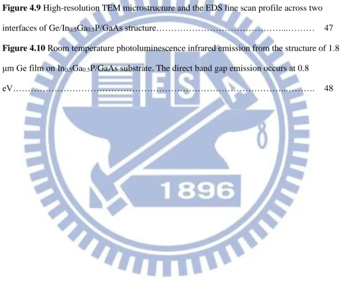
41 4.6 Photoluminescence
N-type doping of Ge will compensate the 0.136 eV difference in energy between Г and L valleys. Figure 4.10 is the room temperature PL infrared emission of 1.8 μm thick Ge
epitaxial layer on In0.5Ga0.5P/GaAs substrate with 330-mW PL incident laser power. The PL
peak at 0.8 eV indicates the electrons in the Г valley recombine with holes in the valence band that makes the direct band-gap emission occur. The emission at the range of 650 to 750 meV is also detected in the spectrum that revealed indirect emission and had much lower intensity. The detection of direct emission in the PL measurement indicates that the defect density of the Ge film is very low. Otherwise, non-radiative recombination due to the large number of defects would decrease the intensity of the L emission.
42
Figure 4.1 (top) Plot of Ge film thickness versus growth time on different surface coverage
InGaP layers. The incubation time are 29.4 and 38.9 minutes for indium coverage of 27.82% and 45.84%, respectively. (bottom) The analysis of composition ratio on InGaP surfaces revealed by XPS 27.82 53.24 18.94 45.84 5.12 49.04 0 10 20 30 40 50 60 In 3d Ga 3d P 2p C om p osit ion r at io on In GaP su rf ace (% ) InGaP (a) InGaP (b)
43
Figure 4.2 Plot of Ge film thickness versus growth time with GeH4 gas flow rate of 10 and 20
sccm, respectively, during growth
Figure 4.3 An illustration of the basic processes of vapor deposition on a surface of a
44
Figure 4.4 Top view surface morphology of Ge grown on In0.5Ga0.5P/GaAs characterized by
45
Figure 4.5 Cross-sectional view surface morphology of Ge grown on In0.5Ga0.5P/GaAs
46
Figure 4.6 Plot of surface roughness and film thickness of Ge versus growth time
47
Figure 4.8 Cross-sectional high-resolution TEM image and diffraction pattern of 190 nm Ge
epitaxial layer
Figure 4.9 High-resolution TEM microstructure and the EDS line scan profile across two
interfaces of Ge/In0.5Ga0.5P/GaAs structure 400 300 Ge InGaP GaAs 200 100 0 0 0.5 1.0 Position (µm) C o u n ts
48
Figure 4.10 Room temperature photoluminescence infrared emission from the structure of 1.8
μm Ge film on In0.5Ga0.5P/GaAs substrate. The direct band gap emission occurs at 0.8 eV.
0.60 0.65 0.70 0.75 0.80 0.85 0.90 0.00E+000 1.00E-012 2.00E-012 3.00E-012 4.00E-012 5.00E-012 6.00E-012 7.00E-012 600 650 700 750 800 850 900 Energy (meV) 0.0 1.0×10⁻¹² 2.0×10⁻¹² 3.0×10⁻¹² 4.0×10⁻¹² 5.0×10⁻¹² 6.0×10⁻¹² 7.0×10⁻¹² P L I n te n si ty ( a. u .) 671nm Laser 300K
49
Chapter 5
Conclusions
High quality epitaxial Ge films were successfully grown on In0.5Ga0.5P/GaAs (100) by
UHVCVD, as confirmed by TEM. This is the first study of Ge grown on InGaP layer to provide with some characteristics of this structure. A longer incubation time is needed for high indium surface coverage of InGaP. The growth mode of Ge on In0.5Ga0.5P/GaAs (100) is
the Volmer-Weber growth, calculated by the thermodynamic theory of capillarity, as well as examined by top-viewed SEM and cross-sectional TEM images. With continuous growth of Ge on InGaP, rough surface would formed as soon as the InGaP surface is completely covered by Ge because the Ge-Ge attachment has lower adatom bonding energy than the formation energy of bonds between Ge and InGaP, resulting in the intensively enhancement of growth rate as well as surface roughness. The main reason is that the surface diffusion is reduced because of high growth rate. As a consequence, for good surface morphology of the Ge film, growth conditions of high temperature and low growth rate are suggested.
The Ge epitaxial film on In0.5Ga0.5P/GaAs (100) has shown sharp interface with
interdiffusion depth as low as the requirement of device applications [25]. And a direct band gap emission at 0.8 eV was detected by PL. This structure studied is useful for the future integration of Ge p-channel and III-V n-channel MOSFETs on the same GaAs template for beyond Si-CMOS logic applications.