國 立 交 通 大 學
電子工程學系 電子研究所碩士班
碩 士 論 文
低電壓差動訊號傳輸標準之
平面顯示器高速資料接收器設計
Design on 1.225 Gb/s LVDS Receiver for
UXGA Flat Panel Display Applications
研 究 生 : 吳建樺
指導教授 : 柯明道 教授
低壓差動訊號標準之
平面顯示器高速接收器設計
Design on 1.225 Gb/s LVDS Receiver for
UXGA Flat Panel Display Applications
研 究 生: 吳建樺
Student : Chien-Hua Wu
指導教授: 柯明道 教授
Advisor : Prof. Ming-Dou Ker
國立交通大學
電子工程學系 電子研究所碩士班
碩士論文
A Thesis
Submitted to Department of Electronics Engineering & Institute of Electronics
College of Electrical Engineering and Computer Science
National Chiao-Tung University
in Partial Fulfillment of the Requirements
for the Degree of
Master
in
Electronics Engineering
Sept. 2005
Hsin-Chu, Taiwan, Republic of China
低電壓差動訊號傳輸標準之
平面顯示器高速資料接收器設計
學生: 吳 建 樺
指導教授: 柯 明 道 教授
國立交通大學
電子工程學系 電子研究所碩士班
ABSTRACT (CHINESE)
摘要
隨著平面顯示器尺寸不斷地增加,顯示器所提供的色彩濃度與解析度也不斷地提 升。解析度SVGA (800× 600 像素) 和 XGA (1024 × 768 像素) 已是平面顯示器最基本 的要求。解析度不斷地提升,同時也意味著資料傳輸量與資料傳送速度的提升。尤其 以位於平面顯示系統裡,直接連接顯示卡到液晶顯示時脈控制器之間的資料傳送遇到 的瓶頸最為明顯。在高速的資料傳送速度下,如何正確地傳送資料成為一個值得研究 的課題。本論文將提出一個應用於平面顯示系統低電壓差動訊號接收器的新架構,提 升資料接受器對訊號偏移量的忍受度,同時降低整個電路的複雜度,達到提高資料接 收效率並節省成本的效果。本文提出的新架構主要分成兩個部份,第一部份中提出三 倍四分之一步距取樣 ( Three quarter steps oversampling ) 架構來提升接收器對輸入訊 號眼圖 ( eye diagram ) 的忍受度。第二部份提出延遲選擇 ( Delay selecting ) 架構來降 低整個接收器佈局的複雜度。傳統接收器架構中,大多使用三倍取樣 ( Three times oversampling ) 架構來恢復 輸入訊號。當輸入資料偏移量接近二分之一步距時,三倍取樣架構將無法分辨出偏移 量是領先還是落後取樣時脈,因此可能造成恢復資料的出錯。本文提出的三倍四分之 一步距取樣中,因為存在一個取樣點落在取樣步距二分之一處,所以在資料偏移量小
於二分之一步距下,三倍四分之一步距取樣架構皆能判斷出資料偏移的方向,達到提 升對眼圖的容忍度。第二部份的延遲選擇架構取代傳統電路中的相位選擇 ( phase selecting ) 架構。傳統的相位選擇架構搭配三倍取樣架構,在平面顯示系統低電壓差 動訊號接收器的應用中,需要使用21 個不同相位的取樣時脈,如此一來將增加電路佈 局的複雜度,連帶造成佈局面積的膨脹。新架構中因為使用延遲選擇架構取代相位選 擇架構,整個電路中只需要使用到7 個不同相位的取樣時脈,大幅減低佈局的複雜度, 同時縮小整個佈局面積達到降低成本的目的。
Design on 1.225 Gb/s LVDS Receiver for
UXGA Flat Panel Display Applications
Student: Chien-Hua Wu
Advisor: Prof. Ming-Dou Ker
Department of Electronics Engineering & Institute of Electronics
National Chiao-Tung University
ABSTRACT (ENGLISH)
ABSTRACT
As the size of flat panel displays increasing, flat panel displays offer higher color depth and resolution. Offering the SVGA (800 × 600 pixels) and the XGA (1024 768 pixels) resolutions becomes a basic requirement of flat panel displays. The increase of display resolution also means the increase of data rate. Especially at the interfaces that directly connect a graphics card to a liquid crystal display’s (LCD’s) timing controller in FPD systems, the high-speed data rate becomes a serious bottle net. When the resolution is up to SXGA (1280 × 1024 pixels) and UXGA (1600
×
× 1200 pixels), the data rate is up to 784 Mbps and 1155 Mbps. How to recover data correctly in the high-speed data rate becomes a significant topic. This thesis is going to present a new architecture of receiver with the LVDS standard for FPD application, which increases the tolerance of the skew between signals and reduces the complexity of the layout. The new architecture not only increases the performance but also reduces the cost. There are tow parts of the new architecture
presented in this thesis. First part presents the “three quarter steps oversampling” system, which increases the tolerance of the eye diagram of input data. Second part presents the “delay selecting,” which reduces the complexity of the layout.
In traditional architecture, most receivers use the “three times oversampling” system to recover input data. However, when the skew between input data and the input clock is close to half step time, the “three times oversampling” system can not detect whether the skew leads or lags, and may induce errors in recovered data. Because there exists a sampling clock phase at the center of data step in the “three quarter steps oversampling” presented in this thesis, the “three quarter steps oversampling” system can detect whether the skew leads or lags when the skew between input data and the input clock is close to half step time. Thus, by using the new system the receiver can increase the tolerance of the eye diagram of input data. The “delay selecting” presented in the second part is used in the receiver instead of the “phase selecting,” which is usually used in traditional architecture. Using the traditional “delay selecting” and “three times oversampling” system in the receiver for FPD applications, it needs 21 differential sampling clock phases to sample input data, and that will increase the complexity of layout and induce the expansion of the layout area. Because the new architecture uses the “delay selecting” instead of the “phase selecting”, it only needs 7 differential sampling clock phases during recovering input data, and that actually reduces the complexity and the area of the layout and reduces the coast of the receiver.
誌謝
ACKNOWLEDGEMENT
首先要感謝的是我的指導教授柯明道博士。老師以其本身嚴謹的研究態度以及超 乎常人的研究熱情,讓我於這兩年中獲得最珍貴的研究心態與方法。而在老師開明的 指導以及豐沛的研究資源下,我不但能盡情將研究的電路下線驗證,也由於所從事的 論文研究具實用性。除此之外,老師亦提供相當充裕的研究經費使我在這兩年中不至 於生活匱乏而能更努力的從事我的碩士論文研究。畢業之後無論從事任何研究我都將 會僅記老師的至理名言:Smart = 做事要有效率,成果要有水準。 接著要感謝的,是一起打拼的同學們,宗信、弼嘉、靖驊、鍵樺、啟祐、吳諭、 家熒、煒明、志朋、峻帆、傑忠、岱原、宗熙、台祐、建文、進元,大家一起做研究, 讓我在苦悶的研究生活中增添不少樂趣。我也要感謝陳世倫學長、陳榮昇學長、張瑋 仁學長、徐新智學長、陳世宏學長、林昆賢學長、黃彥霖學長、鄧至剛學長、顏承正 學長、許勝福學長、王文泰學長。他們無論是在論文研究的瓶頸或是晶片量測的疑難 雜症上都給了我很多的方向及幫助,使我能更順利的完成我的碩士論文。 最後要感謝我的父母。感謝他們多年來默默的關心與支持,在我最需要的時候給 予最大的幫助,使我能勇往向前,一路走來直至今日。生命中的貴人甚多,不可勝數, 我將秉持著感恩的心,盡最大的能力幫助也即將展開論文研究的學弟妹們。 吳建樺 九十四年九月CONTENTS
ABSTRACT (CHINESE)...i
ABSTRACT (ENGLISH) ...iii
ACKNOWLEDGEMENT ... v
CONTENTS ...vi
TABLE CAPTIONS ...viii
FIGURE CAPTIONS...ix
Chapter 1 Introduction ... 1
1.1 MOTIVATION... 1
1.2 THE FPDLINK... 2
1.3 THESIS ORGANIZATION... 3
Chapter 2 Specifications of Low-Voltage Differential Signaling (LVDS) ... 6
2.1 STANDARDS OF LVDS... 6
2.2 INTRODUCTION OF LVDS... 7
2.2.1 Configuration ... 7
2.2.2 Driver Output Levels... 8
2.2.3 Receiver Input Level... 9
Chapter 3 Architecture of Data Recovery System ... 18
3.1 TRADITIONAL DESIGN... 18
3.2.1 Three Times Oversampling... 19
3.2.2 Phase Selecting ... 19
3.2 NEW DESIGN... 22
3.2.1 Three Quarter Steps Oversampling... 22
3.2.2 Delay Selecting ... 24
Chapter 4 Building Blocks of Delay Selecting CDR ... 38
4.1 LVDSINPUT BUFFER... 38
4.2 DELAY SELECTOR... 39
4.4 SYNCHRONIZER AND CONTROL LOGIC...41
4.5 PHASE LOCK LOOP (PLL) ... 43
4.5.1 Phase Frequency Detector ... 44
4.5.2 Charge Pump and Loop Filter... 44
4.5.3 Bias Generator ... 45
4.5.4 VCO and Differential-to-Single-Ended Converter ... 46
Chapter 5 Experiment Results ... 59
Chapter 6 Conclusion and Future Works ... 77
6.1 CONCLUSION...77
6.2 FUTURE WORKS...77
REFERENCES ... 78
TABLE CAPTIONS
Table 1.1 The video resolutions and the corresponding specificity... 4
Table 2.1 LVDS driver specification in general purpose link case ... 12
Table 2.2 LVDS receiver specification in general purpose link case... 13
FIGURE CAPTIONS
Fig. 1.1 A typical serial link and its components...4
Fig. 1.2 A typical FPD Link application...4
Fig. 1.3 The timing relation between input data and input clock in channels ...5
Fig. 1.4 The timing relation between data and clock when skews happen...5
Fig. 2.1 Typical LVDS interface...13
Fig. 2.2 The driver signal level of LVDS for 1.2V VOS...14
Fig. 2.3 The definition of VΔ od and Δ Vos...14
Fig. 2.4 Receiver input signal levels ...15
Fig. 2.5 Receiver hysteresis...15
Fig. 2.6 Vicm input waveform...16
Fig. 2.7 tskew between two receiver inputs ...16
Fig. 2.8 tskew1 between complementary single-ended signals ...17
Fig. 2.9 tskew2 between any parallel signals...17
Fig. 3.1 Typical FPD Link ...27
Fig. 3.2 Timing relation between clock and serial data streams...27
Fig. 3.3 Operation timing in ideal case...28
Fig. 3.4 Operation timing in real cases...28
Fig. 3.5 Operation timing when jitters happen, d0 is double sampled and d1 is missed...29
Fig. 3.6 Operation timing of three times oversampling...29
Fig. 3.7 Operation timing of three times oversampling when skews happen...30
Fig. 3.8 (a) Lag, (b) lead and (c) lock states of three times oversampling ...30
Fig. 3.9 Architecture of a traditional CDR ...31
Fig. 3.10 Timing relation between sampled data...31
Fig. 3.11 Operation of phase detector when jitters happen ...32
Fig. 3.12 Operation of phase selector...32
Fig. 3.13 Data sampling timing when jitters happen...33
Fig. 3.15 Timing relation between VCO cells outputs... 34
Fig. 3.16 Comparison of VCO cells number ... 34
Fig. 3.17 Operation of “three quarter steps oversampling” ... 35
Fig. 3.18 Comparison of eye diagram tolerance in lock state... 35
Fig. 3.19 Operation of the detection window... 36
Fig. 3.20 Architecture of a “delay selecting” CDR... 36
Fig. 3.21 Operation of the “delay selecting” CDR ... 37
Fig. 4.1 Traditional LVDS input buffer... 47
Fig. 4.2 New design of LVDS receiver input buffer ... 47
Fig. 4.3 LVDS receiver input buffer in this thesis ... 48
Fig. 4.4 Simulated frequency response of the LVDS receiver input buffer (Fig. 4.3) ... 48
Fig. 4.5 Architecture of the delay selector ... 49
Fig. 4.6 Schematic diagram of the delay cell... 49
Fig. 4.7 Schematic diagram of the differential to single ended converter ... 50
Fig. 4.8 Simulation result of the delay cells and differential to the single ended converters .. 50
Fig. 4.9 Schematic diagram of the three to one MUX ... 51
Fig. 4.10 Detection window and data sampler... 51
Fig. 4.11 Operation timing of the data sampler ... 52
Fig. 4.12 Schematic diagram and truth table of the phase detector ... 52
Fig. 4.13 Wrong detection results induced by jitters... 53
Fig. 4.14 Schematic diagram of the voter ... 53
Fig. 4.15 State diagram of DLPF ... 54
Fig. 4.16 Schematic diagram of the shift selector... 54
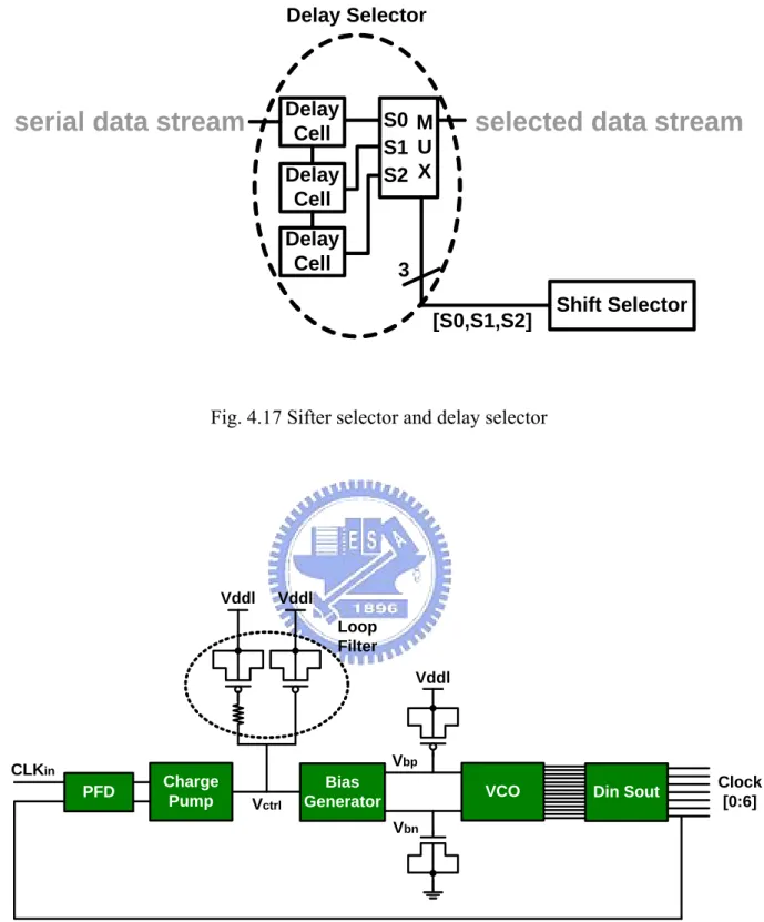
Fig. 4.17 Sifter selector and delay selector ... 55
Fig. 4.18 Architecture of the designed PLL... 55
Fig. 4.19 Schematic diagram of the PFD ... 56
Fig. 4.20 Schematic diagram of the charge pump... 56
Fig. 4.21 Schematic diagram of the loop filter ... 57
Fig. 4.23 Schematic diagram of the VCO ...58
Fig. 4.24 Schematic diagram of the differential-to-single-ended converter...58
Fig. 5.1 Layout and die photo of the tap out test chip ...62
Fig. 5.2 Block diagrams of the serial output test circuit in the tap out test chip ...63
Fig. 5.3 Measurement environment setting of the serial output test...63
Fig. 5.4 Top view of the serial output testing PCB photo...64
Fig. 5.5 Bottom view of the serial output testing PCB photo...64
Fig. 5.6 Cyclic “010101” pattern test result at data rate up to 1.1 Gb/s ...65
Fig. 5.7 Cyclic “010101” pattern test result at data rate up to 1.25 Gb/s ...65
Fig. 5.8 Cyclic “010101” pattern test result at data rate up to 1.8 Gb/s ...66
Fig. 5.9 Cyclic “010101” pattern test result at data rate up to 2 Gb/s ...66
Fig. 5.10 Cyclic “1001001 0110110” pattern test result at data rate up to 1.1 Gb/s ...67
Fig. 5.11 Cyclic “1001001 0110110” pattern test result at data rate up to 1.25 Gb/s...67
Fig. 5.12 Cyclic “1001001 0110110” pattern test result at data rate up to 1.8 Gb/s ...68
Fig. 5.13 Cyclic “1001001 0110110” pattern test result at data rate up to 2 Gb/s ...68
Fig. 5.14 Block diagrams of the parallel output test circuit in the tap out test chip...69
Fig. 5.15 Measurement environment setting of the parallel output test ...69
Fig. 5.16 Top view of the parallel output testing PCB photo ...70
Fig. 5.17 Bottom view of the parallel output testing PCB photo ...70
Fig. 5.18 Test pattern for skew tolerance test ...71
Fig. 5.19 Error recovered data streams when data delay is over skew tolerance ...71
Fig. 5.20 Parallel output testing result when no skew is set in pattern generator ...72
Fig. 5.21 Parallel output testing result when set a 100ps skew in pattern generator...72
Fig. 5.22 Parallel output testing result when set a 150ps skew in pattern generator...73
Fig. 5.23 Parallel output testing result when set a –600ps skew in pattern generator...73
Fig. 5.24 Parallel output testing result when set a –650ps skew in pattern generator...74
Fig. 5.25 Measurement environment setup of the LVDS Link test...74
Fig. 5.26 LVDS Link measurement result at data rate up to 1.15 Gb/s...75
Chapter 1
Introduction
1.1 M
OTIVATIONAs process technologies continue to scale down, the on-chip data rate moves faster than the off-chip data rate. The interface between chips will become a significant bottleneck in high-speed data communication. Thus, how to speed up transmitting data rate over several inches, or even meters between computers or information electrical machines is more and more important.
A typical link (Fig. 1.1) between chips is comprised of three primary components, a transmitter, a channel, and a receiver. In the channel, when the distance between chips is longer, the parasitic effects will become more serious. Under these serious parasitic effects, the frequency of a full swing signal will be limited. Besides, when the data rate of system is up to gigabits-per-second, using a full swing signal to transmit data will induce large power consumption. Therefore, in a high speed and long distance communication how to transmit data is important.
LVDS, low-voltage differential signaling, is one of I/O interfaces usually used in application cases, especially in the data transmission from graphics controller to LCD panels. Due to the specificity of low-voltage swinging, using LVDS I/O interface can not only speed up the data rate, but also reduce the power consumption of I/O interface circuits.
To transmit the internal data into the signal form satisfying the interface specification like LVDS, transmitters in the data communication are needed. Besides, to reduce the number of channels off-chips, each transmitter usually serializes several data from different internal channels into one of these channels off-chips. In some application cases,
transmitters will translate 21 or 28 bits wide TTL data into LVDS data 3 or 4 bits wide and 7 bits deep.
However, how do receivers recover the 3 or 4 bits wide and 7 bits deep LVDS data into 21 or 28 bits wide full swing data correctly, especially when the data rate is up to gigabits-per-second? The parasitic effects in these off-chips channels will induce serious skews and jitters under the high-speed data rate. These receivers need a detecting system to detect these skews and jitters induced by parasitic effects and recover data correctly. In this thesis, a new architecture of the data receiver used in the link with LVDS standard for flap panel display applications is going to be presented.
Table 1.1 lists the resolutions to cope with in this thesis. In this thesis the high resolutions is our main concerns. The receiver presented in this thesis is designed to satisfy the UXGA (1600 × 1200 pixels) resolution, which requires a data rate up to 1155 Mbps and a PLL offering 165MHz clocks.
1.2 T
HEFPD
L
INKFig. 1.2 shows a typical FPD Link (Flat panel Display Link) application. The FPD Link chipset is a family of interface devices specifically configured to support data transmission from graphics controller to LCD panels. The employed technology, LVDS (Low Voltage Differential Signaling), is ideal for high speed and low power data transfer. This enables the implementation of high-end displays.
The FPD Link chipset is composed of a transmitter chip and a receiver chip. The transmitter chip is used to convert the internal data, the output data of graphic card, into LVDS data. After LVDS data are transmitted through the transmission line, the receiver reconverts the LVDS data into internal digital data as the input data of the timing controller.
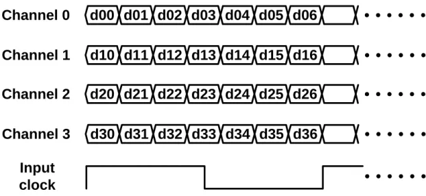
To decrease the number of channels, in application cases, each transmitter would serialize seven different data source into one channel. Therefore, input signal of the receiver is a seven deep LVDS signal. On the other hand, the data rate in each channel is seven times the clock frequency, as shown in Fig. 1.3.
Because of parasitic effects in channels, skews between signals passing channels may occur. Fig. 1.4 shows the timing between input data and the input clock when the skews happen. The receiver must detect the skew between data and the input clock and recover data correctly. In a traditional receiver, three times oversampling is a popular system used to help the receiver detect the skew between data and the input clock. However, in application cases which uses a seven deep serial data as input data, the three times oversampling system needs 21 different sampling clock phases, and that would induce the expansion of the layout area of the PLL (phase lock loop), which provides the receiver 21 different sampling clock phases. To solve this problem, this thesis will present a new detect system using “three quarter steps oversampling” and “delay selecting” instead of “three times oversampling” and “phase selecting” used in the traditional system.
1.3 T
HESISO
RGANIZATIONThe chapter 2 of the thesis would discuss the low-voltage differential signaling (LVDS) standard. The detail DC specifications, signal level and applications of LVDS standard are presented. In the chapter 3, the architecture and implementation of a CDR are discussed. A modified architecture of CDR would be presented and compared with the traditional architecture. The chapter 4 would discuss each building block of the modified architecture presented in chapter 3. How each block is implemented would be presented in this chapter. In chapter 5, the measurement results of the LVDS receiver fabricated in 0.13-μm CMOS process would be present. In chapter 6 are conclusion and future works.
Table 1.1 The video resolutions and the corresponding specificity
Resolutions SVGA XGA SXGA UXGA
Pixels 800 600 × 1024× 768 1280 × 1024 1600 1200 ×
PLL Frequency 40 MHz 65 MHz 112 MHz 165 MHz
Data Rate 280 Mbps 455 Mbps 784 Mbps 1155 Mbps
Internal Data Recovered Data
Clock Rcovery Rx CLK
Tx CLK
Channel
transmit signal receive signal
Transmitter IC Receiver IC
Fig. 1.1 A typical serial link and its components
DRC DRC DRC DRC PLL PLL FPD Link TX Motherboard TFT LCD Panel Graphics Card PC I Bu s Timin g C ont rol le r MUX MUX MU X MU X TFT-LCD Display Column Drivers Ro w D ri v ers FPD Link RX
d30 d31 d32 d33 d34 d35 d36
Input
clock
Channel 3
d20 d21 d22 d23 d24 d25 d26
Channel 2
d10 d11 d12 d13 d14 d15 d16
Channel 1
d00 d01 d02 d03 d04 d05 d06
Channel 0
Fig. 1.3 The timing relation between input data and input clock in channels
d30 d31 d32 d33 d34 d35 d36
Input
clock
Channel 3
d20 d21 d22 d23 d24 d25 d26
Channel 2
d10 d11 d12 d13 d14 d15 d16
Channel 1
d00 d01 d02 d03 d04 d05 d06
Channel 0
Skew between channel 1 and input clock
Fig. 1.4 The timing relation between data and clock when skews happen
Chapter 2
Specifications of Low-Voltage Differential Signaling
(LVDS)
2.1 S
TANDARDS OFLVDS
There are two industry standards that define LVDS [1]. One of the two standards is the generic electrical layer standard defined by the TIA (Telecommunications Industry Association) [2]. This standard is known as ANSI/TIA/EIA-644. The other application specific standard is the standard defined by the IEEE (Institute for Electrical and Electronics Engineering), which is titled SCI (Scalable Coherent Interface) [3]. In this thesis, the receiver is designed following the IEEE standard, SCI.
The original SCI is specified in IEEE standard 1596-1992. The original standard provides computer-bus-like services but uses a collection of fast point-to-point links instead of a physical bus in order to reach far higher speeds. This basic specification defines differential ECL (Emitter Coupled Logic) signals, which provide a high transfer rate (16 bits are transferred every 2 ns). However, because this specification only addressed the high data rates required and didn’t address the low power concerns, this original specification is inconvenient for some applications. Thus, SCI-LVDS specified in IEEE 1596.3 was defined as a subset of SCI. SCI-LVDS specifies signaling levels (electrical specifications) for not only the high-speed but also the low-power physical layer interface. Besides, SCI-LVDS also defines the encoding for packet switching used in SCI data transfers.
2.2 I
NTRODUCTION OFLVDS
The primary goal of IEEE standard for LVDS is to create a physical layer specification for drivers and receivers and signal encoding suitable for use with the SCI as specified by IEEE standard 1596-1992 in low-cost workstation and personal computer applications. In this thesis, because our research focuses on the receiver, following introduction of LVDS will focus on the specification for receivers.
2.2.1 Configuration
Fig. 2.1 shows a typical LVDS interface, which is connected point-to-point. In the LVDS interface, the driver sends a low-voltage swing (400 mV single-ended maximum) differential signal to the receiver with a very high data rate (in IEEE standard for LVDS the data rate is reach 500 Mbits per second per signal pair), and low power dissipation. The power consumption is low because signal swings are small. The LVDS driver drives a minimum 2.5 mA current through a 100-ohm termination resister and switches the direction of current to change the value of data carried by the differential signal. Because the driver load is an uncomplicated point-to-point 100-ohm transmission line environment, the driver can switch the direction of the current through the termination resister in a high speed.
LVDS is independent of the physical layer transmission media. As long as the media deliver the signals to receiver with adequate noise margin and within the skew tolerance range, the interface will be reliable. This is a great advantage when using cables to carry LVDS signals. Sine all connections are point-to-point connected, physical links between nodes are independent of other node connections in the same system. This allows for freedom in developing a useful interconnection that fits the needs of application cases.
In IEEE LVDS standard, the physical environment of point-to-point connections between circuit boards is divided into two cases. First case is for the connections used
between two or more different circuit boards, which must operate with tolerance for Vgpd
(approximately 1 V for 2.5 V powered system). Second case is for the connections used on a PCB or similar environment that will guarantee V
±
gpd is less than 50 mV. In each of
these two different cases, the IEEE LVDS standard has different specification. IEEE LVDS standard calls the first as general purpose link and second case as reduced rang link. In this thesis, because the receiver is designed for a FPD Link, which is used between the motherboard and the TFT LCD panel, all the designs are follow the specification in the general purpose link case.
2.2.2 Driver Output Levels
The output signal of the driver is in a small-swing differential voltage when the driver is properly terminated. Fig. 2.2 shows the differential signal and the relation between the two single-ended outputs. The differential signal is composed of the two single-ended outputs. Because this two single-ended outputs switch alternately, the driver keeps the current constant. The load resistance determines the differential voltage level. In differential application cases the load resistance is different, but in most cases the load resistance is 100-ohm. Fig. 2.2 shows the case where a current source is providing a 4 mA current and the outputs are switching the current at a 50% duty cycle.
Fig. 2.2 also shows the receiver threshold limits in relation to the single-ended signals that arrive at the receiver inputs. When the magnitude of the differential signal is exceeds the threshold voltage, the receiver would determine the logic of input data is switched. In IEEE LVDS standard, a differential voltage grater than or equal to Vidth(max) is a logic high,
and less than or equal to Vidth(min) is a logic low.
In ideal case, the amplitude and common-mode voltage of the steady-state differential signals would not change, but in application case, both of the amplitude and common-mode voltage would change. Thus, IEEE LVDS standard defines the acceptable range of these
changes on signal level. Fig. 2.3 defines the change range of the differential voltage (Δ Vod)
and the driver offset voltage (Δ Vos) in IEEE LVDS standard. Δ Vod and ΔVos can also be
defined in a expression way. Equation (2-1) and equation (2-2) are the definitions of Δ Vod
and ΔVos respectively.
( ) ( )
od od od
V V high V low
Δ = + (2-1)
where
Vod(high)=Voph−Vonl, and Vod(low)=Vonh−Vopl
( ) ( ) os os os V V high V low Δ = + 2 2 (2-2) where
Vos(high) (= Voph−Vonl) / , and Vos(low) (= Vopl −Vonh) /
Table 2.1 shows the detail of the driver specification in general purpose link case in IEEE LVDS standard.
2.2.3 Receiver Input Level
Fig. 2.4 shows the receiver signal level. When the differential input signal is greater than +Vidth, the receiver would detect the input data as logic high. If the input signal were
lower than –Vidth, the receiver would detect the input data as logic low. To eliminate the
possibility of oscillating receiver output signal when the differential input signal is undefined, the threshold hysteresis is needed in receiver design. The undefined input signal may occur when the receiver inputs are unconnected, or when the connected driver is powered down. Fig. 2.5 shows the receiver hysteresis. When the input signal is changing between +Vidth and –Vidth, the receiver would not change the output state.
When the link is operated between two different circuit boards, the different ground-potential may shift the common-mode voltage level. To avoid the error recovered data induced by the different common-mode level happen, the specificity defines an acceptable common-mode voltage range. Fig. 2.6 shows the Vicm waveform. Vicm defined as
the average of Via and Vib measured with respect to the receiver ground potential. Besides
the different potential between driver ground and receiver ground, noise couple between channels would also induce the move of the common-mode level. IEEE standard limits the maximum shift value of common-mode level, and defines the Vicm(max) and Vicm(min) to
limit the range of the input Vicm waveform.
A link system transmitting parallel signals must consider the effect of skews. Because the different channel environments or noise couples, the synchronous signals transmitted through different channels may arriver the receiver in different time. On the other hand, the synchronous signals become asynchronous after transmitted through different channels, and skews between signals must be considered when the receiver recovers these parallel signals. IEEE standard defines the range of skews, and in this rang the receiver must be able to recover data with skews correctly. Fig. 2.7 defined the tskew for propose of IEEE standard.
To set the specificity of signal level more completely IEEE standard defines another two kind of skews for generated differential signal beside tskew. Skew 1 called tskew1 is the skew
between the high-to-low and low-to-high transitions of complementary single-ended signal. Fig. 2.8 shows the definition of tskew1, and equation (2-3) defines tskew1 in expression. Skew
2 called tskew2 is the skew between any differential signals measured at the output of driver.
Fig. 2.9 shows the definition of tskew2, and equation (2-4) defines tskew2 in expression.
1
skew HLA LHB
t = tp −tp or tpHLB−tpLHA (2-3)
to low and low to high.
2 [ ] [ ]
skew diff diff
t = tp i −tp j (2-4)
Where i is any one of the parallel signals and j is any other signal.
Table 2.2 shows the detail of the receiver specification in general purpose link case in IEEE LVDS standard.
Table 2.1 LVDS driver specification in general purpose link case
Symbol Parameter Conditions Min Max Units
Voh Output voltage high, Voa or Vob Rload = 100Ω ±1% 1475 mV
Vol Output voltage low, Voa or Vob Rload = 100Ω ±1% 925 mV
|Vod| Output differential voltage Rload = 100Ω ±1% 250 400 mV
Vos Output offset voltage Rload = 100Ω ±1% 1125 1275 mV
Ro Output impedance, single ended Vcm = 1.0 V and 1.4 V 40 140 Ω
ΔRo Ro mismatch between A & B Vcm = 1.0 V and 1.4 V 10 %
|ΔVod| Change in |Vod| between “0” and “1” Rload = 100Ω ±1% 25 mV
ΔVos Change in Vos between “0” and “1” Rload = 100Ω ±1% 25 mV
Isa, Isb Output current Driver shorted to ground 40 mA
Isab Output current Driver shorted to together 12 mA
|Ixa|, |Ixb| Power-off output leakage Vcc = 0 V 10 mA
Clock Clock signal duty cycle 250 MHz 45 55 %
tfall Vod fall time, 20-80% Zload = 100Ω ±1% 300 500 ps
trise Vod rise time, 20-80% Zload = 100Ω ±1% 300 500 ps
tskew1 Differential skew Any differential pair on package 50 ps
Table 2.2 LVDS receiver specification in general purpose link case
Symbol Parameter Conditions Min Max Units
Vi Input voltage range, Via or Vib |Vgpd| < 925 mV 0 2400 mV
Vidth Input differential threshold |Vgpd| < 925 mV –100 +100 mV
Vhyst Input differential hysteresis Vidhh– Vidhl 25 mV
Rin Receiver differential input impedance –––––– 90 110 mV
tskew
Skew tolerable at receiver input to meet
set-up and hold time requirements Any two package inputs 600 Ω
Interconnect Receiver Driver VO+ V O-VI+ V I-Vgpd 100
Ω
100Ω
LVDS VOA = 1.4 V LVDS VOB = 1 V VOD = +/- 400 mV +/- 800 mV VCM = 0 V VOA - VOB Differential Waveform Vidth (max) Vidth (min) Vidth (max) Vidth (min) 1.4 V 1 V +400 mV -400 mV 0 V diff.
Fig. 2.2 The driver signal level of LVDS for 1.2V VOS
Voa Vob |Vod| Δ GND 0V diff GND Vos Vos Δ 100ΞΩ V Voa Vob Vod = Voa – Vob Vos = (Voa + Vob)/2
+V
od–V
od+V
idth–V
idth undefined logic stateFig. 2.4 Receiver input signal levels
V
out (receiver output single-ended signal)V
idthhV
idthlV
idth (max)V
idth (min)V
in (receiver input differential signal)V
icm(max)
V
icm(min)
V
icmf = 0 Hz to 1 GHz
Fig. 2.6 Vicm input waveform
2 ns
t
skewV
ia[i]
V
ib[i]
V
ia[j]
V
ib[j]
V
id[i]
V
id[j]
t
skew1V
osV
oaV
obFig. 2.8 tskew1 between complementary single-ended signals
t
skew20 V
od0 V
odV
od[i]
V
od[j]
Chapter 3
Architecture of Data Recovery System
3.1 T
RADITIONALD
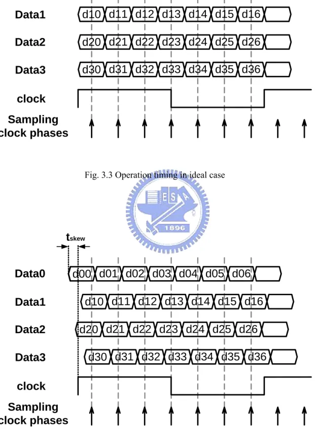
ESIGNIn a typical FPD Link, there are four data channels and one clock channel as shown in Fig 3.1. The driver serializes seven parallel data into one channel. Fig 3.2 shows the timing relation between clock and serialized data. The data rate of each serialized data is seven times the frequency of the clock. However, the different parasitic effect in each channel will induce different time delay and distortion on each transmitted data and clock. Because the different channel effect, these signals will become asynchronous after arrive the receiver. In ideal case, no skews happen after channel effect, the receiver needs only a PLL (phase lock loop) to lock the input clock and proffer seven different data-sampling clock phases and by using these different sampling clock phases the receiver can recover the serial data into seven parallel data with data rate the same as the clock frequency (in FPD Link there are seven different data are serialized in each channel in one clock period). Fig. 3.3 shows the operation timing in the idea case. In application cases, skews between any two signals are unavoidable and the seven different data-sampling clock phases may locate nearly transition edges of the serial data as shown in Fig. 3.4. If the sampling clock phase is near the transition edge, the changing data may be missed or double sampled as shown in Fig 3.5. Thus, to avoid these error data induced by skews happen the recovery system needs an extra mechanism to detect the happen of skews and shift the sampling clock phases away the transition edges of the each serial signal to make sure that these data can be sampled in stable state.
3.2.1 Three Times Oversampling
In traditional design, three times oversampling is usually used in recovery system [4] - [6]. In FPD Link using three times oversampling needs a PLL proffer 21 different sampling clock phases, three times the number of serial data in one clock period. By using these 21 different sampling clock phases, the recovery system can oversample each datum three times as shown in Fig. 3.6. However, when the skews between data and clock happen, the oversampled results of the same datum may be different as the logic state of serial data is changing. Fig. 3.7 shows the sampling timing relation when the skew between serial data and clock happens.
By detecting the different between sampled data sampling the same serial datum, three times oversampling system can detect whether the skew happens or not. Fig. 3.8 shows the timing relation between sampling clock phases and serial data when different skews happen. In Fig. 3.8 (a), as the sampling clock phases lag input serial data stream by a certain amount, data transition might appear between second and third sampled data value within data information set. In Fig. 3.8 (b), if the sampling clock phases lead the input serial data stream by a certain amount, data transition might appear between first and second data value within data information set. In case Fig. 3.8 (c), the input serial data stream is lock by the sampling clock phases, and the first, second and third data value within data information set are the same.
3.2.2 Phase Selecting
Fig. 3.9 shows the architecture of a traditional CDR (clock and data recovery circuit) [4]. It consists of two input buffer, a data sampler, a synchronizer, a phase detector, a voter, a DLPF (digital low pass filter), a phase selector, and a PLL (phase lock loop). One of these two input signal is serial input data in LVDS signal, and another one is input clock in LVDS signal too.
At first, these two input buffer transmit input signals from LVDS signals into full-swing signals. The PLL locks the full-swing input clock and provides the data sampler 21 different sampling clock phases. Because the data rate of input serial data stream is seven times the frequency of input clock, the data sampler uses these 21 different sampling clock phases provided by PLL to sample each serialized datum three times. After data sampler, the input data stream is divided into 21 bits data. However, because these 21 bits data are sampled by different sampling clock phase these 21 bits data translate in different time. On the other hand, the 21 bits data are asynchronous as shown in Fig 3.10. To reduce the complexity of the recovery system, the synchronizer is used to synchronize the 21 bits asynchronous data.
By comparing every three sampled data of each serial datum, the phase detector can detect if any serial datum is lagged or leaded. If one datum were detected lead or lag, the first sampled result is different from the second and third sampled results or the third result is different from the first and second results, the phase detector would send a signal “up” or “down” in a couple bits, one “up” bit and one “down” bit, as the phase detecting result of this datum. Thus, in each clock period the phase detector would send out seven couple bits as detecting result signals of these seven serial data respectively.
However, because the effect of jitters these seven detecting result signal would not always the same. For example, one “up” result and three “down” results appear in one clock period as shown in Fig. 3.11. After the phase detector is a voter. The voter would receive seven couple bits from the phase detector in every clock period. Each couple bits carry the detection information of one serial datum in this clock period. By comparing these “up” bits and “down” bits in these seven couple bits, the voter must determine whether the input serial data stream leads the input clock or lags. If the “up” signals is over tow bits more than the “down” bits, the voter would send out another “up” signal. On the other hand, if the “down” signals are over two bits more than the “up” bits, the voter would send out another
“down” signal.
In application cases, the effect of jitters is serious and that means the jitters disperse in a large rang. Thus the voter is not enough to avoid the wrong “up” or “down” signal induce by the effect of jitters. To increase the jitter tolerance of the CDR, after voter the “up” or “down” signal must pass the DLPF, that means the DLPF would not let the “up” or “down” signal pass unless the “up” or “down” bit must keep in high logic for three consecutive clock periods at least. If the “up” or “down” bit keeps in high logic over three consecutive clock periods the DLPF would send out anther real “up” or “down” signal.
The phase selector would receive a couple of bits, one real “up” bit and one real “down” bit, in every clock period. If the DLPF pass a real “up” signal to the phase selector, the phase selector would accept the detection that the input serial data stream leads these 21 sampling clock phases and shift up these 21 different sampling clock phases one phase let faster sampling clock phases sample the input serial data stream in next clock period. Similarly, if the DLPF pass a real “down” signal to the phase selector, the phase selector would accept the detection that the input serial data stream lags these 21 sampling clock phases and shift down these 21 different sampling clock phases one phase let slower sampling clock phases sample the input serial data stream in next clock period. Fig. 3.12 shows the operation of the phase selector.
These detecting system will keep shifting these data sampling clock phases up or down until there are no real “up” and real “down” signals are send into the phase selector and that mean the three times oversampling is in lock state. Fig. 3.13 shows the timing relation between the input serial data stream and the input clock in lock state. In lock state, when jitters happen the first sampled datum and third sampled datum may be an error datum that sampled in wrong datum but the second sampled datum would keep the same logic stat with the sampled datum because the second sampling clock phase would still be kept in the right datum. Thus, the CDR would select each second sampled result as the recovered datum of
each serial datum and send out these seven recovered data in parallel as the output of the CDR.
Besides, to differentiate the new architecture of CDR presented in following from the traditional design, the architecture of a traditional CDR is called “phase selecting”.
3.2 N
EWD
ESIGN3.2.1 Three Quarter Steps Oversampling
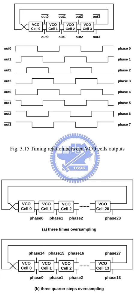
Fig. 3.14 shows a typical architecture of a PLL. The number of VCO cells in a PLL is determined by the number of phases the PLL must provide. Besides, in application cases, these VCO cells are usually designed in fully differential and that can increase the stability of the PLL. Because these VCO cells are fully differential, these inverted phases can be used as the output phases of the PLL when the number of phase the PLL must provide is an even number. Thus, if a PLL is required to provide n phases where n is an even number, the PLL can use only n/2 VCO cells to provide n different phases dispreading in one clock period uniformly. Fig. 3.15 shows the relation between output phases of the VCO cells and output phases of the PLL when the PLL must provide 8 different phases in one clock period. However, if the PLL must provide odd number phases, the PLL can’t use these inverted phases of VCD as output phases and a PLL providing n number phase where n is an odd number must use n VCO cells to provide these output phase the PLL must provide.
In application cases of FPD Link, because the input data stream is 7 bits deep signal serialized in one clock period, the PLL must provide 21 different sampling clock phases to implement three times oversampling. Because 21 is an odd number, the PLL can not use these inverted phases of VCO cells as a part of these 21 different sampling clock phases. Thus, in three times oversampling the PLL must use 21 VCO cells to provide 21 different sampling clock phases dispreading uniformly in one clock period and that would make the
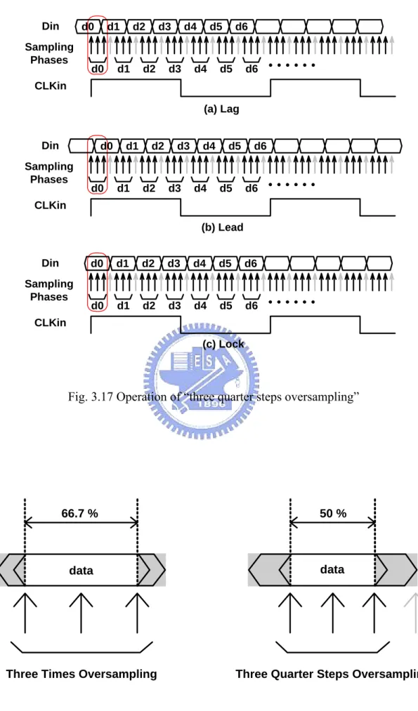
layout area of the PLL expand. However, the VCD is the primary part in the layout area of the PLL. To reduce the problem this thesis presents a modified process, which is called “three quarter steps oversampling”, to recover data.
In “three quarter steps oversampling” the PLL provides 28 different sampling clock phases dispreading uniformly in one clock. Because there is seven data are serialized in one clock, there are four different sampling clock phases in ever data step and each distance between every two adjacent phases is equate to a quarter data step time. To detect the locations of skews between input data stream and input clock the “three quarter steps oversampling” would select three of these four phases in each data step to oversample each datum. Because each datum is oversampled three times and each distance between every two adjacent sampling clock phases is equate to a quarter step time, this modified process which is used to recover data is called “three quarter steps oversampling”. Because the PLL in “three quarter steps oversampling” provides 28 different sampling clocks phases where 28 is an even number, the PLL can use only 14 VCO cells to provide these sampling clock phases. Thus, the number of VCO cells used in “three quarter steps oversampling” is less than that used in “three times oversampling”. On the other hand, the layout area of the PLL used in “three quarter steps oversampling” will be smaller than the PLL used in “three times oversampling”. Fig. 3.16 shows the VCO cells of the PLL used in “three quarter steps oversampling” and “three times oversampling” respectively.
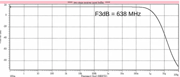
Fig 3.17 shows the operation of the “three quarter steps oversampling”. By using 21 of these 28 different sampling clock phases provided by the PLL, the CDR could detect whether the sampling clock phases lag input data stream or lead. If the sampling clock phases lag the input data stream as shown in Fig. 3.17 (a), the CDR would shift up these sampling clock phases one phase. If the sampling clock phases lead the input data stream as shown in Fig. 3.17(b), the CDR would shift down these sampling clock phases one phase. The CDR would keep shifting these sampling clock phases until the input data stream is
locked by these sampling clock phases as shown in Fig. 3.17 (c).
Besides the improvement of reducing the layout area of PLL, the “three quarter steps oversampling” also has higher tolerance of input data eye diagram. Fig. 3.18 shows the timing relation between the eye diagram of the input data stream and the sampling clock phases in the “three quarter steps oversampling” case and the “three times oversampling” case respectively. In “three quarter steps oversampling” the CDR can keep in lock state when the eye diagram of the input data stream closes nearly 50%, but in “three times oversampling” the eye diagram of the input data stream must open over 60% to keep the CDR in lock state.
3.2.2 Delay Selecting
Three quarter steps oversampling does reduce the size of PLL, but it also has another problem. There are only 21 phases used to sample data when three times oversampling is used, but there will be 28 phases used to sample data when three quarter steps oversampling is used. Using more different phases to sample data will make the layout of CDR more complex. Besides, because the sampling clock phases used in three quarter steps oversampling is more than that used in three times oversampling, the three quarter steps oversampling CDR need more MUXs to implement the motion of selecting sampling clock phases.
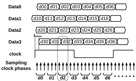
To overcome this problem, a new architecture of a CDR is presented in following. Besides using three different sampling clock phase oversample data stream, using the same sampling clock phase sample three different delayed data can also detect the happen of skews too [9]. By using VCO cells as delay cell, the CDR can delay input data stream one phase, two phases, and three phases respectively. Using these three the same data streams delayed one phase, two phases, and three phases as a detection window, the CDR can use one sampling clock detect whither the edge happens in this windows as shown in Fig. 3.18.
If there is any edge happens in the detection window, the CDR will change the delayed time up or down one phase in next clock period.
Fig. 3.19 shows the operation of delay selecting. If the edge happens between the data delayed one phase and the data delayed two phases, the delay time of input data stream would be decrease one phase in next clock period. If the edge happens between the data delayed two phases and the data delayed three phases, the delay time of input data stream would be increase one phase in next clock period. The delay time would be changed until there no edge happens in the detection window.
Fig. 3.20 shows the architecture of the delay selecting CDR. To implement the operation of delay selecting, the CDR use VCD cells as delay cells create three data stream delayed in different phased. One of these three delayed data streams would be selected and the selected stat stream would be sent into the detection window. In the detection window the selected data stream is delayed into three different delayed data streams again. In detection window the CDR can use only seven different sampling clock phases to sample these three data stream and detects whether any edge happen. The detection window would send out “up” and “down” signals in every clock period. The same as the phase selecting CDR, these “up” and “down” signal must pass a voter and a DLPF. After passing the voter and the DLPF, if a real “up” or “down” signal is send out, the delay selector would change the selected data stream up or down as shown in Fig. 3.21. If the skew is over a data step time the information between input signals is not enough to detect whither the skew is a lead skew or a lag one. To avoid this undetected skew, LVDS specificity would limit the skew range between every two different channel. Because the skew range between every two different channel is limited in one data step time, the delay selector only need three different delay timing, one phase delay, two phases delay, and three phases delay, to be selected to cancel the skew.
reduce the number of sampling clock phases from 28 to 7 and also reduce the number of MUXs. On the other hand, the layout area is reduced and simplified.
DRC DRC DRC DRC PLL PLL FPD Link TX Motherboard TFT LCD Panel Graphics Card PCI Bus Timing Con trolle r MU X MUX MU X MU X TFT-LCD Display Column Drivers Row Driver s FPD Link RX Data0 Data1 Data2 Data3 Clock
Fig. 3.1 Typical FPD Link
d30 d31 d32 d33 d34 d35 d36
clock
Data3
d20 d21 d22 d23 d24 d25 d26
Data2
d10 d11 d12 d13 d14 d15 d16
Data1
d00 d01 d02 d03 d04 d05 d06
Data0
d00 d01 d02 d03 d04 d05 d06
d10 d11 d12 d13 d14 d15 d16
d20 d21 d22 d23 d24 d25 d26
d30 d31 d32 d33 d34 d35 d36
clock
Data3
Data2
Data1
Data0
Sampling
clock phases
Fig. 3.3 Operation timing in ideal case
d00 d01 d02 d03 d04 d05 d06
d10 d11 d12 d13 d14 d15 d16
d20 d21 d22 d23 d24 d25 d26
d30 d31 d32 d33 d34 d35 d36
clock
Data3
Data2
Data1
Data0
Sampling
clock phases
t
skewjitter
d0
d1
d2
data stream
sampling
phases
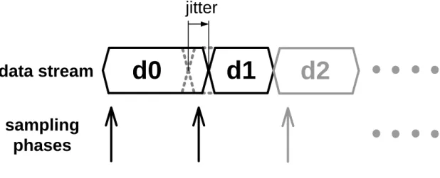
Fig. 3.5 Operation timing when jitters happen, d0 is double sampled and d1 is missed
d00 d01 d02 d03 d04 d05 d06
d10 d11 d12 d13 d14 d15 d16
d20 d21 d22 d23 d24 d25 d26
d30 d31 d32 d33 d34 d35 d36
clock
Data3
Data2
Data1
Data0
Sampling
clock phases
d00 d01 d02 d03 d04 d05 d06 d10 d11 d12 d13 d14 d15 d16 d20 d21 d22 d23 d24 d25 d26 d30 d31 d32 d33 d34 d35 d36 clock Data3 Data2 Data1 Data0 Sampling clock phases d0 d1 d2 d3 d4 d5 d6 tskew
Fig. 3.7 Operation timing of three times oversampling when skews happen
d0 d1 d2 d3 d4 d5 d6 d0 d1 d2 d3 d4 d5 d6 CLKin Din Sampling Phases d0 d1 d2 d3 d4 d5 d6 d0 d1 d2 d3 d4 d5 d6 CLKin Din Sampling Phases d0 d1 d2 d3 d4 d5 d6 d0 d1 d2 d3 d4 d5 d6 CLKin Din Sampling Phases (a) Lag (b) Lead (c) Lock
Data Sampler Input Buffer Synchronizer Phase Detector Voter DLPF Phase Selector Input Buffer PLL 21 7 7 28/21 28/21 28/21 CLK 7 Dout Din+ Din-CLK+ CLK-21
Fig. 3.9 Architecture of a traditional CDR
Data sampled by phase0 Data sampled by phase1
Data sampled by phase2 Data sampled by phase3
Data sampled by phase17 Data sampled by phase18
Data sampled by phase19 Data sampled by phase20 CLK
d0
d1
d2
d3
d4
d5
d6
d0
d1 d2
d3 d4
d5
d6
down down up down
jitter data sampling phases clock Output of phase detector
Fig. 3.11 Operation of phase detector when jitters happen
d0 d1 d2 d3 d4 d5 d6 d0 d1 d2 d3 d4 d5 d6 d0 d1 d2 d3 d4 d5 d6 d0 d1 d2 d3 d4 d5 d6 CLKin Din Sampling Phases
(a) phases shift up
(b) phases shift down
d0 d1 d2 d3 d4 d5 d6 Sampling Phases in next clock d0 d1 d2 d3 d4 d5 d6 CLKin Din Sampling Phases Sampling Phases in next clock
jitter
d0
jitter
d00input data
sampled data
sampling phases
d01 d02Fig. 3.13 Data sampling timing when jitters happen
PFD
Charge
Pump
Bias
Generator
CLKin VDD VDD 21 Sampling Clock Phases VCO Cell 0 VCO Cell 1 VCO Cell 2 VCO Cell 20VCO
VCO Cell 0 VCO Cell 1 VCO Cell 2 VCO Cell 3 out0 out0 out1 out1 out2 out2 out3 out3 out0 out1 out2 out3 out0 out1 out2 out3 phase 0 phase 1 phase 2 phase 3 phase 4 phase 5 phase 6 phase 7
Fig. 3.15 Timing relation between VCO cells outputs
VCO Cell 0 VCO Cell 1 VCO Cell 2 VCO Cell 13 phase13 phase2 phase1 phase0 phase27 phase16 phase15 phase14 VCO Cell 0 VCO Cell 1 VCO Cell 2 VCO Cell 20 phase20 phase2 phase1 phase0
(b) three quarter steps oversampling (a) three times oversampling
d0 d1 d2 d3 d4 d5 d6 CLKin d0 d1 d2 d3 d4 d5 d6 Din Sampling Phases d0 d1 d2 d3 d4 d5 d6 CLKin d0 d1 d2 d3 d4 d5 d6 Din Sampling Phases d0 d1 d2 d3 d4 d5 d6 CLKin d0 d1 d2 d3 d4 d5 d6 Din Sampling Phases (a) Lag (b) Lead (c) Lock
Fig. 3.17 Operation of “three quarter steps oversampling”
data 50 %
data 66.7 %
Three Times Oversampling Three Quarter Steps Oversampling
CLKin d0 d1 d2 d3 d4 d5 d6 Detection window Sampling Phases (b) Lead d0 d1 d2 d3 d4 d5 d6 d0 d1 d2 d3 d4 d5 d6 CLKin d0 d1 d2 d3 d4 d5 d6 Detection window Sampling Phases (a) Lag d0 d1 d2 d3 d4 d5 d6 d0 d1 d2 d3 d4 d5 d6 CLKin d0 d1 d2 d3 d4 d5 d6 Detection window Sampling Phases (c) Lock d0 d1 d2 d3 d4 d5 d6 d0 d1 d2 d3 d4 d5 d6 clk0 clk1 clk2 clk3 clk4 clk5 clk6 clk0 clk1 clk2 clk3 clk4 clk5 clk6 clk0 clk1 clk2 clk3 clk4 clk5 clk6
Fig. 3.19 Operation of the detection window
clock d0 d1 d2 d3 d4 d5 d6 d0 d1 d2 d3 d4 d5 d6 d0 d1 d2 d3 d4 d5 d6 select stream 1 d0 d1 d2 d3 d4 d5 d6 d0 d1 d2 d3 d4 d5 d6 d0 d1 d2 d3 d4 d5 d6 d0 d1 d2 d3 d4 d5 d6 d0 d1 d2 d3 d4 d5 d6 d0 d1 d2 d3 d4 d5 d6 d0 d1 d2 d3 d4 d5 d6 d0 d1 d2 d3 d4 d5 d6 d0 d1 d2 d3 d4 d5 d6 select stream 2 select stream 0 stream 1 stream 0 stream 2 Detection Window Delay Selector up up down down up up down down sampling phases clk0 clk1 clk2 clk3 clk4 clk5 clk6
Chapter 4
Building Blocks of Delay Selecting CDR
Fig. 3.20 shows the architecture of the delay selecting CDR. These building blocks of the delay selecting CDR would be presented in this chapter.
4.1 LVDS
I
NPUTB
UFFERFig. 4.1 shows a traditional design of a LVDS receiver buffer. The differential input signal is detected by the Schmitt trigger (M1 ~ M6 and M7 ~ M10), which translates the detected signal into the full swing output Vout. However, in this receiver buffer the lower
bound of input signal common mode range is limited by M3 and M4. In IEEE LVDS standard the specificity of the LVDS levels at the receiver input are (4-1) and (4-2).
100 idth V ≥ mV 0mV ≤ ≤Vi 2400mV (4-1) (4-2)
Thus, when the common mode voltage of input signal is close to 0mV, M1 and M2 in Fig. 4.1 would enter into the triode region to keep the Vgs of M4 and M5 over Vth. Because
M1 and M2 operate in triode region, the voltage gain of this design in Fig. 4.1 would be significantly reduced.
To overcome this problem of input common mode range in Fig. 4.1, a new LVDS receiver buffer is reported [10]. Fig. 4.2 shows the new design. To solute the problem in traditional design, the new design is cascoded another buffer, first stage buffer, before the Schmitt trigger. The voltage gain of the first stage buffer is almost insensitive to the input
signal common mode voltage. Because the differential signal after the first stage is almost irrelevant to the input common mode voltage, the Schmitt trigger can be implemented in NMOS type, which has better frequency response the PMOS type. However, in reference [10] the new designed receiver input buffer is implemented in 3.3V devices. In the thesis the LVDS CDR is implemented in 0.13 mμ 1.2V / 3.3V CMOS process. In order to translate the input signal from the 3.3V LVDS signal into a 1.2V full swing signal, the receiver input buffer in this thesis is implemented in 1.2V, Vddl, beside the current source supporting current to M1 and M2 is connect to 3.3V, Vddh, as shown in Fig. 4.3. Concerning in the problem of gate oxide reliability the first stage buffer M1 ~ M6 must designed in 3.3V device.
To receive a high speed input signal the frequency response of the receiver input buffer is important. If the receiver must receive a signal in 1.25 Gb/s, the frequency response bandwidth of the input buffer must higher than 625 MHz. To make sure the frequency response bandwidth is higher enough, the bias voltages Vb1, Vb2 and impedance value of R1
and R2 is important. Fig. 4.4 shows the frequency response simulation result of the LVED
receiver input buffer designed in this thesis.
4.2 D
ELAYS
ELECTORAfter input buffer input data signal is translated from 3.3V LVDS signal into full swing 1.2V digital serial data stream. This serial data stream would be send into the delay selector. Fig. 4.5 shows the architecture of delay selector. Delay selector is composed of three delay cells and one three to one MUX. By using these three delay cells the input serial data stream is delayed into three different time delayed data streams. One of these three different time delayed data streams would be selected according to the operational code send from the shift selector. Fig. 4.6 shows the circuit of the delay cell. Controlling bias voltage at Vbp and
Vbn, the pull up and pull down current of the delay cell would be changed. According to
different pull current, the delay cell can make the input signal delayed in different time. To make sure each delay time is equal to a quarter data step, the delay cell is design in the same scale with the VCO cell in the PLL and the bias voltages Vbp and Vbn is also provide by the
PLL.
The signals after delay cells are differential and not a full swing signal. To pull these signals into full swing single ended signal, a different to single ended converter is needed. Fig. 4.7 shows the different to single ended converter. Fig. 4.8 shows the simulation result of the delay cells and differential to single end converters. After delay cells and differential to single end converters, the send out signals, D0 ~ D2, are full swing data streams delayed in different phases respectively. The delay selector would select one of these three data stream to cancel the skew between the input data stream and the clock. A three to one MUX is used to select the correct data stream. Fig. 4.9 shows the schematic diagram of the three-to-one MUX.
4.3 D
ETECTIONW
INDOW ANDD
ATAS
AMPLERAfter the delay selector the selected data stream would be send into the detection window. The detection window is composed of three delay cells, which is the same as that used in the delay selector. In the detection window the selected data stream would be delayed in different phases. After detection window these data stream delayed in different phases would be sampled by different sampling clock phases in data sampler as shown in Fig. 4.10. By sampling these delayed data streams the CDR can get the logic state of the input data stream at different moment. Fig. 4.11 shows the timing relation between sampled data streams, sampling clock phases, and sampling results.
4.4 S
YNCHRONIZER ANDC
ONTROLL
OGICAs shown in Fig. 4.11 the sampling results, D0 ~ D20, are asynchronous. To simplify the circuit after the sampler in this CDR a synchronizer is used to synchronize these sampling results. These synchronized data stream would be send into control logic. In control logic a phase detector is used to detect whether a skew happen in the detection window. Fig. 4.12 shows the schematic diagram of the phase detector and the truth table of the phase detector. If the input signal of the phase detector is “001” or “110” the phase detector would assume that in this detection window a translation edge happens in the data stream behind the center sampling clock phase and sends out a “down” signal to ask the delay time of the selected data stream lag a quarter step time in next clock period. On the contrary, if the input signal of the phase detector is “100” or “011” the phase detector would assume that in this detection window a translation edge happens in the data stream before the center sampling clock phase and sends out a “up” signal to ask the delay time of the selected data stream lead a quarter step time in next clock period.
Besides the skews between data stream and the clock signal the jitter in data stream would make the phase detector send out “up” or “down” signal too. As the result, this requirement sent out by the phase detector would not be accepted immediately and a voter and a DLPF (digital low pass filter) are used to analysis these “up” and “down” signals and verify that a skew between the data stream and the clock signal really happens.
Because there are seven data be serialized into the input data stream during each clock period, the CDR need seven phase detectors to detect whether any translation edge happen in each data step. In another word, there would be seven detection results sent out in each clock period. If a skew really happen between the data stream and the clock these seven detection results should be the same or no detection result, no edge happen in this data step. However, the fitter in the data stream would make some wrong detection result as shown in