High sensitivity carbon monoxide sensors made by zinc oxide modified gated
GaN/AlGaN high electron mobility transistors under room temperature
S. C. Hung, C. W. Chen, C. Y. Shieh, G. C. Chi, R. Fan, and S. J. Pearton
Citation: Applied Physics Letters 98, 223504 (2011); doi: 10.1063/1.3596440 View online: http://dx.doi.org/10.1063/1.3596440
View Table of Contents: http://scitation.aip.org/content/aip/journal/apl/98/22?ver=pdfcov Published by the AIP Publishing
Articles you may be interested in
Characteristics of carbon monoxide sensors made by polar and nonpolar zinc oxide nanowires gated AlGaN/GaN high electron mobility transistor
Appl. Phys. Lett. 103, 083506 (2013); 10.1063/1.4818671
SnO2-gated AlGaN/GaN high electron mobility transistors based oxygen sensors J. Vac. Sci. Technol. B 30, 041214 (2012); 10.1116/1.4736974
Carbon monoxide detection sensitivity of ZnO nanorod-gated AlGaN/GaN high electron mobility transistors in different temperature environments
J. Vac. Sci. Technol. B 30, 010606 (2012); 10.1116/1.3672010
Effect of humidity on hydrogen sensitivity of Pt-gated AlGaN/GaN high electron mobility transistor based sensors
Appl. Phys. Lett. 96, 232106 (2010); 10.1063/1.3454279
Oxygen gas sensing at low temperature using indium zinc oxide-gated AlGaN/GaN high electron mobility transistors
J. Vac. Sci. Technol. B 28, 376 (2010); 10.1116/1.3368467
This article is copyrighted as indicated in the article. Reuse of AIP content is subject to the terms at: http://scitation.aip.org/termsconditions. Downloaded to IP: 140.113.38.11 On: Wed, 30 Apr 2014 09:08:01
High sensitivity carbon monoxide sensors made by zinc oxide modified
gated GaN/AlGaN high electron mobility transistors under room
temperature
S. C. Hung,1,a兲C. W. Chen,2C. Y. Shieh,3G. C. Chi,4R. Fan,5and S. J. Pearton6
1Optical Science Center, National Central University, Jhong-Li 320, Taiwan 2Department of Physics, National Central University, Jhong-Li 320, Taiwan 3
Department of Optics and Photonics, National Central University, Jhong-Li 320, Taiwan
4
Department of Photonics, National Chiao Tung University, Hsinchu 300, Taiwan
5
Department of Chemical Engineering, University of Florida, Gainesville, Florida 32611, USA
6
Department of Material Science and Engineering, University of Florida, Gainesville, Florida 32611, USA
共Received 7 April 2011; accepted 10 May 2011; published online 3 June 2011兲
AlGaN/GaN high electron mobility transistors共HEMTs兲 with zinc oxide 共ZnO兲 nanowires modified gate exhibit significant changes in channel conductance upon expose to different concentration of carbon monoxide 共CO兲 at room temperature. The ZnO nanowires, grown by chemical vapor deposition共CVD兲 with perfect crystal quality will attach CO molecules and release electrons, which will lead to a change in surface charge in the gate region of the HEMTs, inducing a higher positive charge on the AlGaN surface, and increasing the piezoinduced charge density in the HEMTs channel. These electrons create an image positive charge on the gate region for the required neutrality, thus increasing the drain current of the HEMTs. The HEMTs source-drain current was highly dependent on the CO concentration. The limit of detection achieved was 400 ppm in the open cavity with continuous gas flow using a 50⫻50 m2gate sensing area. © 2011 American Institute
of Physics.关doi:10.1063/1.3596440兴
Recently, metal oxide semiconductors, such as SnO2,
In2O3, ZnO, indium tin oxide, and magnesium zinc oxide, play important roles in a lot of areas of chemistry, physics, and material science.1–5In these candidates, ZnO is a semi-conductor with direct band gap energy of 3.37eV at room temperature and large binding energy of 60 meV. So, it is a promising material for optoelectronics devices, such as light emitting diodes 共LEDs兲, solar cell, and transparent contact layer, and gas sensors.6–9The utilization of ZnO in gas sen-sor application has a long history. Devices composed of ZnO were studied as chemoresistive materials to detect gases like H2, NH3, CH4, O2, trimethylamine, ethanol, and CO.10–16
Carbon monoxide 共CO兲 is one of the most dangerous gases in air pollution and human daily life. CO is produced by incomplete combustion of fuels and commonly found in the emission of automobile exhausts, the burning of domestic fuels, etc. It is highly toxic and extremely dangerous because it is colorless and odorless. CO sensors are, therefore, needed in various situations including the detection of smoldering fires. It is believed that the sensing mechanism is based on the reaction between adsorbed oxygen molecules on the sur-face of ZnO and the gas molecules was detected by changing the electrical properties of ZnO. Thus, a lot of research groups are devoted in studying the relations between differ-ent surface morphology, such as nanowire, nanorods and nanobelts, and sensitivity. However, recently reports show a nano-ZnO sensor prepared by an arc plasma method did not show an expected high sensitivity even when exposed to CO at a concentration as high as 5000 ppm.17
Recently, AlGaN/GaN high electron mobility transistors 共HEMTs兲 have shown great potential for chemical and bio-chemical sensing applications.18–29 This is due to their high
electron sheet carrier concentration channel induced by both piezoelectric and spontaneous polarization. Unlike conven-tional semiconductor field effect transistors, there is no in-tentional dopant in the AlGaN/GaN HEMTs structure. The electrons in the two-dimensional electron gas共2DEG兲 chan-nel are located at the interface between the AlGaN layer and GaN layer, and there are positive countercharges at the HEMT surface induced by the 2DEG. Slight changes in the ambient can affect the surface charge of HEMTs, thus chang-ing the 2DEG concentration in the channel. Thus, nitride HEMTs may be excellent candidates for gas sensors applica-tions.
In this letter, we study the effect of CO concentration on the drain current of AlGaN/GaN HEMTs sensors with ZnO nanowire modified gate. We quantified the sensitivity, the temporal resolution, and the limit of detection of these sen-sors for CO detection.
The ZnO nanowire used to function the gate area were grown on c-plane GaN by chemical vapor deposition共CVD兲. Zinc shot 共99.9999% pure兲 and O2 共99.9999% pure兲 were
used as precursors for Zn and O, respectively. The growth details were reported in Ref.30. The characterization of ZnO nanowires were studied by photoluminescence 共PL兲 mea-surement with a continuous wave He–Cd 325 nm laser, x-ray diffraction共XRD兲 using Cu K␣1radiation, scanning electron
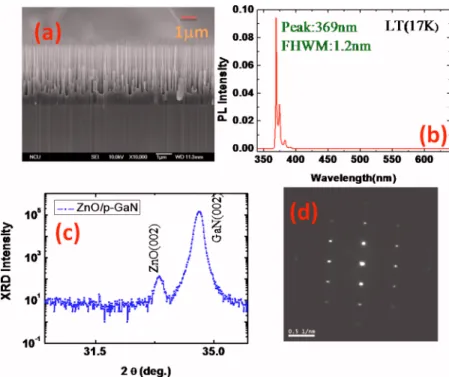
microscope 共SEM兲, and selected area diffraction patterns 共SADPs兲, respectively. As shown in Fig. 1共a兲, the diameter and length of ZnO nanowires are very uniform and about 80 nm and 3.5 m, respectively. Low temperature PL spec-trum indicate strong band-edge emission with FWHM is 1.2 nm and weak impurity band emission, as shown in Fig.1共b兲, Fig. 1共c兲shows single 共002兲 orientation of ZnO nanowires grown on 共002兲 GaN by XRD. The SADP data shows an excellent crystalline quality and corresponds to ZnO共002兲.
a兲Electronic mail: shengchun@ufl.edu.
APPLIED PHYSICS LETTERS 98, 223504共2011兲
0003-6951/2011/98共22兲/223504/3/$30.00 98, 223504-1 © 2011 American Institute of Physics
This article is copyrighted as indicated in the article. Reuse of AIP content is subject to the terms at: http://scitation.aip.org/termsconditions. Downloaded to IP: 140.113.38.11 On: Wed, 30 Apr 2014 09:08:01
The HEMT structures consisted of a 2 m thick un-doped GaN buffer and 250 Å thick unun-doped Al0.25Ga0.75N cap layer. The epilayers were grown by metal-organic CVD on thick GaN buffers on sapphire substrates. Mesa isolation was performed with inductively coupled plasma共ICP兲 etch-ing with Cl2/Ar discharges at ⫺90 V dc self-bias, ICP power
of 300 W at 2 MHz, and a process pressure of 5 mTorr. 50 ⫻50 m2 Ohmic contacts separated with gap of 50 m consisted of e-beam deposited Ti/Al/Pt/Au patterned by lift-off and annealed at 850 ° C for 45 s under a flowing N2. AZ
1818 positive photoresist was used as the mask to define the gate area for ZnO nanowires coating, and the gate dimension was 50⫻50 m2.
For coating ZnO nanowires on the gate area, the ZnO nanowires on GaN template were put into the ethanol solu-tion and the solusolu-tion was stirred and ultrasonic for 10 min in order to break the connection between ZnO nanowires and GaN template. After ultrasonication, the homogenous ZnO nanowires ethanol solution was dripped onto the gate area by micropipette and dried at 85 ° C for 5 min using a hot plate. Figure 2 shows the schematics of HEMTs sensor coated with ZnO nanowires. For the CO sensing measurement, the HEMTs sensor was mounted on a carrier and put in a gas chamber which filled by N2gas. The temperature of chamber
was keep at room temperature and a constant drain bias volt-age of 500 mV was applied to the drain contact of the sensor. Finally, different amounts of CO gas were injected into the chamber. Figure 3 shows the real time CO detection with ZnO modified gate HEMTs. The drain current of the HEMT sensor showed a rapid increase when the CO concentration
was changed to 1600 ppm in the open cavity with continuous gas flow. A further decrease in the drain current for the HEMT sensor was observed when the CO concentration de-creased to 400 ppm. These abrupt drain current increases were due to the change in charges in the ZnO nanowires upon a shift in CO concentration. A HEMT sensor without the ZnO nanowires on the gate area was loaded in the gas chamber, and there was no change in drain current observed. It is well accepted that the sensitivity of semiconductor gas sensors is attributed to the chemisorptions of oxygen on the oxide surface and the subsequent reaction between ad-sorbed oxygen and tested gas, which caused the resistance change. The same mechanism may be applied for the CO-sensing of the present ZnO nanowires gated HEMTs. Thus, more CO molecules can react with more oxygen species on the ZnO nanowire surface, and in this letter, we emphasis the electrical change via measuring the change in drain current in the HEMTs instead of measuring the change in resistance. Takata et al.30 found that the stable oxygen ion were O2− FIG. 1. 共Color online兲 共a兲 SEM image of ZnO nano-wires on GaN template.共b兲 PL spectrum of ZnO nano-wires under 17 K.共c兲 XRD spectrum of ZnO nanowires on GaN template.共d兲 SADP data of ZnO nanowires.
FIG. 2. 共Color online兲 Schematic of ZnO nanowires gated HEMT sensor.
FIG. 3.共Color online兲 Drain current of a ZnO nanowires gated AlGaN/GaN HEMT as a function of different CO gas flow rate.
223504-2 Hung et al. Appl. Phys. Lett. 98, 223504共2011兲
This article is copyrighted as indicated in the article. Reuse of AIP content is subject to the terms at: http://scitation.aip.org/termsconditions. Downloaded to IP: 140.113.38.11 On: Wed, 30 Apr 2014 09:08:01
below 100 ° C, O−between 100 and 300 ° C, and O2−above
300 ° C. The relevant reactions on the surface area could be as follows:
2CO + O2−→ 2CO2+ e−, 共1兲
CO + O−→ CO2+ e−, 共2兲
CO + O2−→ CO2+ 2e−. 共3兲
From the knowledge of the catalytic activity, it is anticipated that reducing agents will react rapidly with O−presented on
the surface but very slowly with O2−. So, normally at a low temperature below 150 ° C, the ZnO based CO sensor show low response in previous work.31–33 In this work, we utilize ZnO nanowires with excellent crystal quality to adsorb CO species and release electron on the ZnO nanowire surface, which will induced more positive charge on the AlGaN sur-face and enhance the current going through the drain and source contact even at room temperature.
The CO sensor showed a good repeatability, as illus-trated in Fig.4, the drain current response of the ZnO nano-wires gated HEMT sensor to CO gas flow rate was switching from 0 to 400 ppm. The change in drain current for the HEMT exposed between 0 to 400 ppm was still considerably larger than the background noise. Thus, HEMTs could be used to detect small difference in CO concentration.
In conclusion, ZnO nanowires gated AlGaN/GaN HEMTs showed rapid change in the source-drain current when exposed to different CO concentration ambient at room temperature. These results show the potential of ZnO nano-wire gated AlGaN/GaN HEMT for CO sensing applications. This work was supported by the National Science Coun-cil of Taiwan under Grant No. NSC97-2112-M-008-016-MY3.
1D. H. Yoon and G. M. Choi,Sens. Actuators B 45, 251共1997兲. 2M. C. Horrillo, A. Serventi, D. Rickerby, and J. Gueierrez,Sens. Actuators
B 58, 474共1999兲.
3C. A. Papadopoulos, D. S. Vlachos, and J. N. Avaritsiotis,Sens. Actuators
B 42, 95共1997兲.
4G. Sberveglieri, G. Faglia, S. Groppelli, and P. Nelli,Sens. Actuators B 8,
79共1992兲.
5T. Seiyama and S. Kagawa,Anal. Chem. 38, 1069共1966兲. 6T. Alammar and A. V. Mudring,Mater. Lett. 63, 732共2009兲. 7J. Zhang, W. Yu, and L. Zhang,Phys. Lett. A 299, 276共2002兲. 8O. Lupan, L. Chow, and G. Chai,Sens. Actuators B 141, 511共2009兲. 9C. Li, Z. Du, H. Yu, and T. Wang,Thin Solid Films 517, 5931共2009兲. 10B. Bott, T. A. Jones, and B. Mann,Sens. Actuators 5, 65共1984兲. 11H. Nanto, T. Minami, and S. Takata,J. Appl. Phys. 60, 482共1986兲. 12M. Egashira, N. Kanehara, Y. Shimizu, and H. Iwanaga,Sens. Actuators B
18, 349共1989兲.
13G. Sberveglieri, P. Nelli, and S. Groppelli, Mater. Sci. Eng., B 7, 63
共1990兲.
14H. Nanto, H. Sokooshi, and T. Kawai,Sens. Actuators B 14, 715共1993兲. 15F. Paraguay D., M. Miki-Yoshida, J. Morales, J. Solis, and L. W. Estrada,
Thin Solid Films 373, 137共2000兲.
16J. D. Choi and G. M. Choi,Sens. Actuators B 69, 120共2000兲.
17L. F. Dong, Z. L. Cui, and Z. K. Zhang,Nanostruct. Mater.8, 815共1997兲. 18G. M. Chertow, E. M. Levy, K. E. Hammermeister, F. Grover, and J.
Daley,Am. J. Med. 104, 343共1998兲.
19A. P. Zhang, L. B. Rowland, E. B. Kaminsky, V. Tilak, J. C. Grande, J.
Teetsov, A. Vertiatchikh, and L. F. Eastman,J. Electron. Mater. 32, 388 共2003兲.
20B. S. Kang, H. T. Wang, F. Ren, S. J. Pearton, T. E. Morey, D. M. Dennis,
J. W. Johnson, P. Rajagopal, J. C. Roberts, E. L. Piner, and K. J. Linthi-cum,Appl. Phys. Lett. 91, 252103共2007兲.
21O. Ambacher, M. Eickhoff, G. Steinhoff, M. Hermann, L. Gorgens, V.
Werss, B. Baur, M. Stutzmann, R. Neuterger, J. Schalwig, G. Muller, V. Tilak, B. Green, B. Schafft, L. F. Eastman, F. Bernadini, and V. Fiorien-bini, Proc.-Electrochem. Soc. 3, 335共2002兲.
22B. S. Kang, H. T. Wang, T. P. Lele, Y. Tseng, F. Ren, S. J. Pearton, J. W.
Johnson, P. Rajagopal, J. C. Roberts, E. L. Piner, and K. J. Linthicum, Appl. Phys. Lett. 91, 112106共2007兲.
23R. Neuberger, G. Muller, O. Ambacher, and M. Stutzmann,Phys. Status
Solidi A 185, 85共2001兲.
24J. Schalwig, G. Muller, O. Ambacher, and M. Stutzmann, Phys. Status
Solidi A 185, 39共2001兲.
25H. T. Wang, B. S. Kang, F. Ren, S. J. Pearton, J. W. Johnson, P. Rajagopal,
J. C. Roberts, E. L. Piner, and K. J. Linthicum, Appl. Phys. Lett. 91, 222101共2007兲.
26G. Steinhoff, M. Hermann, W. J. Schaff, L. F. Eastman, M. Stutzmann, and
M. Eickhoff,Appl. Phys. Lett. 83, 177共2003兲.
27B. S. Kang, H. T. Wang, F. Ren, B. P. Gila, C. R. Abernathy, S. J. Pearton,
J. W. Johnson, P. Rajagopal, J. C. Roberts, E. L. Piner, and K. J. Linthi-cum,Appl. Phys. Lett. 91, 012110共2007兲.
28S. C. Hung, B. H. Chou, C. Y. Chang, C. F. Lo, K. H. Chen, Y. L. Wang,
S. J. Pearton, A. Dabiran, P. P. Chow, G. C. Chi, and F. Ren,Appl. Phys. Lett. 94, 043903共2009兲.
29S. C. Hung, Y. L. Wang, B. Hicks, S. J. Pearton, D. M. Dennis, F. Ren, J.
W. Johnson, P. Rajagopal, J. C. Roberts, E. L. Piner, K. J. Linthicum, and G. C. Chi,Appl. Phys. Lett. 92, 193903共2008兲.
30C. W. Chen, C. J. Pan, F. C. Tsao, Y. L. Liu, G. C. Chi, C. Y. Chang, and
T. H. Hsueh,ECS Trans. 25共12兲, 113 共2009兲.
31M. Takata, D. Tsubone, and H. Yanagida, J. Am. Ceram. Soc. 59, 4
共1976兲.
32J. Xu, Q. Pan, Y. Shun, and Z. Tian,Sens. Actuators B 66, 277共2000兲. 33J. F. Chang, H. H. Kuo, I. C. Leu, and M. H. Hon,Sens. Actuators B 84,
258共2002兲. FIG. 4. 共Color online兲 Drain current of a ZnO nanowire gated AlGaN/GaN
HEMT as a function of different CO gas flow rate.
223504-3 Hung et al. Appl. Phys. Lett. 98, 223504共2011兲
This article is copyrighted as indicated in the article. Reuse of AIP content is subject to the terms at: http://scitation.aip.org/termsconditions. Downloaded to IP: 140.113.38.11 On: Wed, 30 Apr 2014 09:08:01