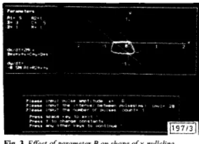
x and y directions can be arihtrarily adjusted by combining the variation of B and C .
3 MACGRFGOR, K. J., and LEWIS, E. R . ’ ‘Neural modeling‘ (Plenum Press, New York and London, 1976)
4 FITZHUGH, R.. ‘Impulses and physiological States in theoretical models of nerve membrane’, Biophp J.. 1961, I , pp. 4 4 - 4 6 6 5 MEAUER, J. L., et ul.: ‘Programmable impulse neural circuits’, I E E t
Trans. Neural Netw., 1991,2, pp 101 108
6 M U R R A Y , A. F., et ul : ‘Pulse-stream V L S l neural networks mixing analog and digital technique,’. I E E E Tran, Neurul . Y m . , 1991. 2, pp. 193-204
7 HORN, U,, and USHER, M.: ‘Neural networks with dynamical thresh- olds’, Phys. Rev. A , 1989,40, pp. 1036-1044
8 YANAI. H., et ul.: ‘Associative memory network composed of neurons with hysteretic property’, Neurul Nerw., 1990, 3, pp 223- 228
9 SANCHEZ-SINENCIO, t.: ’Guest editorial -~ neural network circuit implementations’, I E E E Trans. Neural Nrtw., 1990, 2, p. 192 10 VANTONEN, K., et al.: ‘Pulse-stream neural networks and reinforce-
ment learning’. Proc. IJCNN ‘90, San Diego. 1990,2, pp. 267-272 Fig. 3 Effect ofparameter B on shape of x-nullcline
The effect of parameter M can be clearly observed from the curves of x and y against time, as shown in Fig. 4. Parameter M only affects the refractory period, and exerts no influence on the amplitudes of x and y and the threshold. When M increases, the refractory period is linearly shortened, otherwise it is extended.
INTERACTION OF COBALT AND FIELD OXIDE DURING LOW TEMPERATURE FURNACE ANNEALING
B.-S. Chen and M.-C. Chen
Inderrng rerm, Annruliny, Semiconductor deri<e.s and motermly
Fig. 4 Effect of parameter M on refractory period Refractory period can he arbitrarily adjusted by varying M
Discussion. A neuron model with dynamically adjustable threshold, refractory period and response amplitude is pro- posed, which meets the needs of pulse-stream neural nets. The above analysis shows that the parameters in eqns. 1 and 2 have an obvious impact on the performance of the model. We can adjust the parameter values to make the model satisfy any given performance, whereas it is impossible to do so in the FitrHugh-Nagumo model. For example, parameters B and C are first adjusted to guarantee the amplitudes of x and y . Next, A , and A , are adjusted to select suitable equilibrium point. We can then adjust D to select any given threshold. Finally, M can be adjusted to select the required refractory period.
There are still problems in the learning of pulse-stream neural nets. It was noted that reinforcement learning is suit- able for training this type of neural network [IO]. The authors think that evolutionary learning or genetic algorithms are potential candidates. We have applied nets composed of the neurons described by eqns. I and 2, trained through evolu- tionary learning, to solve the XOR problem. In the experi- ment, the input and output are encoded into pulses, ‘I’ is represented by pulse signal of a certain frequency, and ‘0 is represented by a signal without pulses. The experiment shows promising results.
24th February 1992 Q Gan and Y. Wei (Department of Biomedical Engineering, Southeast Universify, Nunjing. 210018, People’s Republic of China)
References
1 MCCULLOCH, W. S., and PITTS, w.: ‘A logical calculus of the ideas imminent in servous activity’, Bull. of Math. Biophys., 1943, 5, pp 115-133
2 HninxiN, A L., and HUXLFY, A. F.: ‘A quantitative description of membrane current and its applications to conduction and excita- tion i n nerve’. J OJ Physiology, 1952, 117, pp. 500-544
756
The interaction of cobalt and thermally grown held oxide (5m.A) during low temperature furnace annealing (600- 800-C) is described. I t is found that the isolation functior of oxide becomes unreliable and s-pit clusters from in the silicon substrate when the annealing temperature exceeds 7WC. Therefore, i t is essential to limit the first annealing temperature of the selfaligned silicide scheme below 600 C.
Introduction. Metal silicides selectively formed on the source/ drain regions have received much attention because they can alleviate many problems encountered in submicrometre CMOS process and because of their selfaligned nature. Among the silicides, CoSi, is one of the most promising candi- dates for salicide (selfaligned silicide) schemes due to its low resistivity and high temperature stability [I]. In addition, the absence of CO-As or CO-B pair formation [Z], ease of selective etching and good chemical stability during processing offer further attractive reasons for the employment of cobalt silicide in CMOS technology. The thermal stability of cobalt on oxide during heat treatment is one of the decisive factors in deter- mining the first annealing temperature of the salicide scheme. The interaction of CO with SiO, has been reported [3-51. It was concluded that CO does not react with SiO, below 900-C in accordance with several material analysis techniques, such as AES and T E M . In this work, the interaction of CO and oxide at a lower temperature ( ~ 8 0 o ’ C ) was examined by the delineation of saucer pits ( S pits). In addition, the electrical property of the field oxide was evaluated using current-voltage (I-V) characteristics.
Eyperiment . The starting material was (IOO)-oriented, phosphorus-doped n-type silicon wafers with 17- 50R-cm nominal resistivity. Immediately after RCA cleaning, a 5000
A
oxide layer was thermally grown by pyrogenic oxidation. After oxidation. four different processes were performed to prepare the samples. Sample set A was deposited with 500of cobalt film in an e-beam evaporation system at a base pres- sure less than 5 x IO-’ torr and with a deposition rate of 1 . k s . Without breaking the vacuum, a 50A of r-Si film was deposited on top of the CO film to serve as a passivation layer for the subsequent heat treatment. The preparation of the simple set B was the same as that of sample set A except that cobalt film of 40A thick with a deposition rate of 0.5 A/s was deposited. For sample set C, only 50A of 1-Si was deposited ELECTRONICS LETTERS 9th April 1992 Vol 28 NO 8
on the oxide. Sample set D was used as a control and n o deposition process was performed after oxidation. T h e four sample sets were then annealed in an N, ambient for 600, 700 a n d 800°C. T h e annealing time was 30 min.
To investigate the electrical a n d material properties of the systems, all sample sets were divided into two categories. O n e half
of
each sample was used to prepareMOS
diodes for studying the electrical properties of the oxide. Unreacted C O a n d / o r cobalt silicide were removed by wet etching a n d theMOS diodes were fabricated by the deposition of AI dots. T h e other halves of the samples were processed as follows. First, all the deposited films a n d the thermally grown field
(500A)
oxide on the silicon substrate were removed by various a p p r o - priate etching solutions. T h e samples were then sent through a 1025-C pyrogenic oxidation cycle for
2
h after standard RCA cleaning. It has been reported that S pits can be observed after oxidation if the silicon substrate is contaminated by cobalt metal [6]. T h eS
pits can be observed after the oxide is stripped a n d the silicon substrate is given a delineation etch such as in Secco [7-81. In this study, the samples were delin- eated by Secco etch forS
min with ultrasonic agitation. T h e surface after Secco delineation was inspected bySEM.
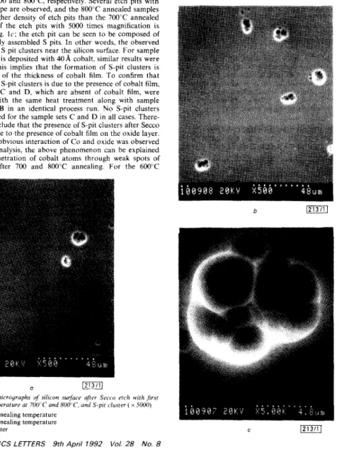
Results: Fig. la a n d h present SEM micrographs of the silicon surface after Secco etching for sample set A with annealing atperformed 700 and XWC, respectively. Several etch pits with irregular shape are observed, a n d the 800°C annealed samples exhibit a higher density of etch pits than the 700°C annealed ones. One of the etch pits with
5000
times magnification is shown in Fig.IC;
the etch pit can be seen to be composed ofseveral locally assembled S pits. In other words, the observed etch pits ar e S pit clusters near the silicon surface. F o r sample set
B,
which is deposited with 4 0 A cobalt, similar results were observed. This implies that the formation of S p i t clusters is independent of the thickness of cobalt film. To confirm that the origin of S p i t clusters is due to the presence of cobalt film, sample sets C and D, which are absent of cobalt film, were processed with the same heat treatment along with sample sets A and B in an identical process run. No S-pit clusters were observed for the sample sets C a n d D in all cases. There- fore, we conclude that the presence of S-pit clusters after Secco etching is d u e t o the presence of cobalt film on the oxide layer. Because no obvious interaction of CO a n d oxide was observed from AES analysis, the above phenomenon can be explained by local penetration of cobalt atoms through weak spots ofthe oxide after 700 a n d 800°C annealing. For the 600°C
annealing, no S-split cluster was found for all four sets of samples. Th e above results indicate that the temperature for the first annealing should be limited to 6WC.
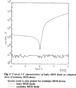
T h e current-voltage (I-V) characteristics of the MOS diodes were measured on 30 test sites, with a diode area of 0.01 cm', for sample set A. T h e results are summarised in Table
1.
It is obvious that higher temperature annealing leads to unreliable oxide isolation properties. T h e failure sites typically exhibit significant leakage current as shown in Fig.2.
This result indicates that the leakage paths in the oxide have been con- structed by the penetration of cobalt atoms. T h e instability of the isolation function of oxide will cause the problem of lowering the device yield. Therefore, the first annealing tem- perature of the salicide scheme exceeding 700°C is a n obstacleto maintaining the integrity of the isolation function of the field oxide.
A modified process was used to evaluate the influence of ion implantation. Following a 200A CO and a subsequent
50A
Z-Si deposition on the SiO,(SUOUA)/Si substrate, As+ ions
were implanted into the x-Si/Co(SiO,/Si structure to a dose of 5 x 1 0 ' 5 c m - 2 at XOkeV. Ion implantation was employed to intermix cobalt and oxide at the interface. T h e implanted samples underwent the same process sequence as that of sample set A for
MOS
fabrication and S-pit cluster delin- eation. No evidence of oxide deterioration and S-pit clusterFig. 1 S t M micrographs of silicon surface afirr Srcco annealing remperature ar 700°C and XOOC, and S-pit clu.
a 700-C annealing temperature h 800°C annealing temperature c S p i t cluster
erch n,irh Jirsr Yter ( x 5000)
C
augmentation was observed. This indicates that ion implanta- tion does not affect the quality of the field oxide.
, n o
F I
- 4 2 0 2 4
bias,V
pg
Fig. 2 Typical I-V characteristics of leaky MOS diode as compared t o those ofnonleaky M O S device
System noise is only present for nonleaky MOS device
_ _ _ _ leaky MOS diode
___ nonleaky MOS diode
In conclusion, it is found that direct silicidation above 700°C will degrade the performance of the field oxide and induce S-pit clusters in the silicon substrate. For samples annealed at 600°C, none of the above problems is observed. Thus, the first annealing of the salicide scheme below 600°C is a prerequisite for obtaining reliable processing of the a-Si/Co/SiO,/Si structure during heat treatment.
Table 1 FREQUENCY O F FAILURE SITES AND S-PIT CLUSTERS OF SAMPLE SET A AFTER VARIOUS FIRST ANNEALING
CONDITIONS
~~
Sample set A 600°C 700°C 800°C
Percent of failure sites 0 0-3.3% 0-6.7%
no yes Yes
S-pit clusters
A c k n o w l e d g m e n t s : This work is supported by the National Science Council, ROC, under contract No. NSC-80-040-E- 009-15.
25th February 1992
B.-S. Chen and M.-C. Chen (Department of Electronics Engineering and the Institute of Electronics, National Chiao-Tung University, 1001 Ta-Hsueh Rd., Hsinchu, Taiwan, 300, Republic of China)
References
1 MURAKA, s. P.: ‘Silicides for VLSI applications’ (Academic Press, New York, 1983)
PROBST, v.: ‘Degradation of doped-Si regions contacted with transition-metal silicides due to metaldopant compound forma- tion’, J. Appl. Phys., 1989.66, pp. 5327-5334
DECLERK, c.: The use of CoSi, as compared to TiSi, for a self- aligned technology’, IEEE Symp. VLSI Technology, 1987, pp. 67-68
4 CHEN, w. D., CUI, Y. D., mu, c. c., and TAO, I.: ‘Interaction on CO with Si and SiO, during rapid thermal annealing’, J. Appl. Phys., 1991,69, pp. 7612-7619
5 MORGAN, A. E., BROADBENT, E. K.. DELFINO, M., COULMAN, B., and SADANA, D. K.: ‘Characterization of a self-aligned cobalt silicide process’, Electrochem. Soc., 1987,134, pp. 925-935
6 GAFF, K., and PIEPER, H.: ‘The behavior of transition and noble metals in silicon crystals’, Semiconductor Silicon, 1981, pp. 331-343 2 MAEX, K., DE KEERSMAECKER, R. F., GHOSH, G., D E W , L., and
3 VAN DE HOVE, L., W0LTF.W R., MAEX, K., DE KERSMAECKER, R., and
758
7 SECCO O’ARAWNA, F.: ‘Dislocation etch for (100) planes in silicon’, J. Electrochem. Soc., 1972,119, pp. 948-951
8 MOSS, T. s. (Ed.): ‘Handbook on semiconductors’ (North Holland, New York, 1980)
NONLINEAR CONTlN UOUS-PH ASE
FREQUENCY SHIFT KEYING
R.
Liyanapathirana,S.
Le-Ngoc and N. Ekanayake Indexing terms: Modulation, Frequency shift keying, Digital communication systemsSeveral nonlinear trellis modulation codes based on multi- level continuous-phase frequency-shift keying (M-CPFSK) are presented. On additive white Gaussian noise channels these digital FM schemes achieve higher minimum Euclidean distances and memory lengths than conventional CPFSK signals.
Introduction: Continuous-phase frequency-shift keying (CPFSK) has gained interest over other digital modulation schemes because of its phase continuity property [2, 31. The inherent memory of CPFSK signals improves spectral per- formance and also enables maximum-likelihood sequence detection using the Viterbi algorithm [5]. The asymptotic error probability of CPFSK signals operating over the clas- sical Gaussian channel at high signal to noise ratio is given by P ,
=,
Q [ J ( d & J 2 N 0 ) ] , where d , , is the normalised minimum Euclidean distance corresponding to all possible merging events of the finite-state trellis of the system. N , / 2 is the double-sided noise power spectral density and Q ( x ) = [1/J(2n):
j
e - y 2 i z d y . The performance of CPFSK signals can be improved by increasing the minimum Euclidean distance.In the literature, techniques such as multi-h signalling [3], partial response signalling [l], and convolutional precoding [6] have been shown to increase the minimum Euclidean dis- tance. Recently, a novel binary nonlinear multi-h CPFSK sig- nalling technique [4] has been introduced where the state transition matrix is realised by adaptively changing the modu- lation index of the signals. Research reported in this Letter follows a similar strategy to increase the minimum Euclidean distance, but instead of binary multi-h signals, it uses single4 multilevel FSK signals. The numerical results obtained for nonlinear 4-CPFSK and nonlinear 8-CPFSK indicate that they achieve higher minimum Euclidean distances than the conventional M-CPFSK signals. Several schemes have been found to achieve the maximum memory length v,, allowed by the number of trellis phase states. For a system with N states, vmr is equal to L1
+
logzNJ[4], whereL(
)I
indicates the largest integer less than or equal to ( ).Nonlinear continuous-phase F S K : Consider M-CPFSK with rational value modulation index h = p/q. where p and q are relatively prime positive integers. The state transition matrix
T,
of such a system is a q by q matrix with elements a, (a. E {k
1, k 3 , k 5 , ..., f(M
- 1))) and Os corresponding to the presence or absence of paths between the q phase states:0, 211h. 4nh,
....
2(M - 1)nh (modulo-2n). For example, the finite-state system of h = 1/4,4-CPFSK con- sists of the four phase states 0, 4 2 , II, 3n/2 and has the state transition matrixThe rows and columns of T4 correspond to the phase angles in the reverse order. Therefore row one of T4 corresponds to the ELECTRONICS LETTERS 9th April 1992 Vol. 28 No. 8