360 IEEE ELECTRON DEVICE LETTERS, VOL. 27, NO. 5, MAY 2006
High-Performance Poly-Silicon TFTs
Using HfO
2
Gate Dielectric
Chia-Pin Lin, Student Member, IEEE, Bing-Yue Tsui, Senior Member, IEEE, Ming-Jui Yang, Ruei-Hao Huang,
and Chao-Hsin Chien, Associate Member, IEEE
Abstract—High-performance low-temperature poly-Si thin-film transistors (TFTs) using high-κ (HfO2) gate dielectric is
demon-strated for the first time. Because of the high gate capacitance den-sity and thin equivalent-oxide thickness contributed by the high-κ gate dielectric, excellent device performance can be achieved including high driving current, low subthreshold swing, low threshold voltage, and high ON/OFF current ratio. It should be noted that theON-state current of high-κ gate-dielectric TFTs is almost five times higher than that of SiO2 gate-dielectric TFTs. Moreover, superior threshold-voltage (Vth) rolloff property is also demonstrated. All of these results suggest that high-κ gate dielectric is a good choice for high-performance TFTs.
Index Terms—Hafnium dioxide (HfO2), high dielectric-constant dielectric, thin-film transistors (TFTs).
I. INTRODUCTION
L
OW-TEMPERATURE poly-Si (LTPS) thin-film transis-tors (TFTs) have been used as pixel and driving ICs in active-matrix liquid crystal displays (AMLCDs) [1]. Recently, to realize system-on-panel (SOP), integrating driving ICs on the glass substrate are required [2]. However, it is a challenge to de-velop high-performance TFTs for both pixel TFTs and driving circuits [3]. To drive the liquid crystal, pixel TFTs operate at high voltages with low gate-leakage currents. In contrast, high-speed display driving circuits require TFTs to operate at low voltages and high driving currents, with a low threshold voltage. Using a thin gate oxide can increase the driving current of TFTs. Unfortunately, for a conventional gate dielectric (i.e., SiO2 or Si3N4), a thinner gate dielectric may induce highergate-leakage current and degrade the TFT characteristics sig-nificantly [4]. In the previous studies, to preserve the physical gate-dielectric thickness while increasing the gate capacitance density and then improving the mobile carrier density in the channel region, several new high-κ gate-dielectric materials including Al2O3and Ta2O5were suggested [5], [6]. However,
the κ value of Al2O3 is 9–10 and is not high enough, and the
improvement of the device performance is not apparent [7]. On the other hand, due to narrowbandgap, it is necessary to use a thick Ta2O5 as gate dielectric in TFTs to reduce the
gate-Manuscript received January 3, 2006; revised February 17, 2006. This work was supported by the National Science Council, Taiwan, R.O.C. under Contract NSC-93-2215-E-009-004. The review of this letter was arranged by Editor J. Sin.
C.-P. Lin and B.-Y. Tsui are with the Department of Electronics Engineering and Institute of Electronics, National Chiao-Tung University, Hsinchu 300, Taiwan, R.O.C. (e-mail: [email protected]).
M.-J. Yang, R.-H. Huang and C.-H. Chien are with the National Nano Device Laboratories, Hsinchu 300, Taiwan, R.O.C.
Digital Object Identifier 10.1109/LED.2006.872832
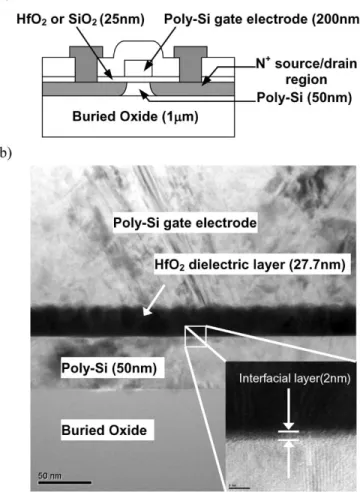
Fig. 1. Cross-sectional (a) drawing and (b) TEM of the proposed high-κ HfO2 gate-dielectric TFT structure.
leakage current [8]. Therefore, the increase of gate capacitance density is limited. Recently, hafnium dioxide(HfO2) becomes a
candidate of future high-κ gate-dielectric material in MOSFET due to its high-κ value (∼ 25), widebandgap, acceptable band alignment, and superior thermal stability with poly-Si [9], [10]. In this paper, we integrated high-κ HfO2 gate dielectric with
TFTs for the first time.
II. DEVICEFABRICATION
Fig. 1(a) and (b) shows the schematic drawing of the HfO2gate-dielectric TFT and the cross-sectional transmission
electron microscopy (TEM) micrograph of the gate struc-ture, respectively. The fabrication started by depositing a 50-nm amorphous Si (α-Si) layer at 550◦C in a low-pressure 0741-3106/$20.00 © 2006 IEEE
LIN et al.: HIGH-PERFORMANCE POLY-SILICON TFTs USING HfO2GATE DIELECTRIC 361
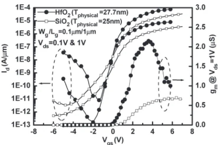
Fig. 2. Output characteristics of the TFTs using HfO2 or SiO2 as gate dielectric.
chemical vapor deposition (LPCVD) system on Si wafers capped with a 1-µm thick thermal oxide layer. The deposited α-Si layer was then recrystallized by solid phase crystalliza-tion (SPC) process at 600 ◦C for 24 h in a N2 ambient.
Next, in order to fabricate narrow-width devices to enhance the gate controllability and reduce the influence of grain-boundary defects, electron beam lithography (EBL) and reac-tive ion etching (RIE) were used to pattern the device acreac-tive islands [11], [12]. The narrowest channel width is 0.1 µm. Then, after removing the native oxide by dipping in diluted hydrofluoric acid (HF) solution, an HfO2 thin film was
de-posited in a metal–organic CVD (MOCVD) system at 400◦C as gate dielectric. Oxygen and Argon were used as reactant and transmission gases with flow rates of 1000 and 200 sccm, respectively. The total pressure in the chamber is fixed at 5 mbar and the injection frequency is 3 Hz. Another 200-nm α-Si layer was deposited at 550 ◦C in an LPCVD system
and then was patterned to form gate electrode. Because of the thermal budget during the α-Si gate deposition, the thick amor-phous HfO2 layer became polycrystalline structure, and then
formed the rough top interface between gate electrode layer and HfO2 film. Next, a self-aligned phosphorous ion implantation
was performed at 60 keV to a dose of5 × 1015cm−2to dope
source/drain region and gate electrode. After a 300-nm-thick HF passivation layer was deposited by a plasma-enhanced CVD (PECVD) system at 300◦C, the contact holes were patterned by a two-step wet-etching process. First, the 300-nm oxide layer was etched by buffered oxide etch (BOE) solutions. Then, to raise the HfO2/SiO2selectivity, the HfO2films were etched by
an isopropyl alcohol (IPA):HF mixture [13]. Additional anneal-ing for dopants’ activation was performed at 600◦C for 12 h in an N2ambient. Finally, typical Al metallization completed the
fabrication process. In order to enhance the device performance, an NH3plasma treatment at 350◦C for 30 min was performed
to passivate the defect states before measurements [14]. For comparison, poly-Si TFTs with a 25- and 45-nm tetra-ethoxy-silane (TEOS) SiO2deposited by an LPCVD system were also
fabricated with the same process flow.
Fig. 3. Transfer characteristics of the TFTs using HfO2 or SiO2 as gate dielectric.
TABLE I
DEVICEPARAMETERS OFTFTSWITH27.7-nm HfO2OR
25-nm SiO2ASGATEDIELECTRIC ATVds= 0.1 V
Device performance was measured using an Agilent 4156 C semiconductor parameter analyzer and an Agilent 4284 A impedance analyzer. The threshold voltage is defined as the gate voltage at which the drain current reaches 100 nA∗ Wg/Lg,
where Lg is the drawn channel length and Wg is the drawn
channel width. Effective mobility is extracted from the maxi-mum transconductance(gm).
III. RESULTS ANDDISCUSSION
According to Fig. 1(b), the physical thickness of HfO2films
is equal to 27.7 nm, and the interfacial SiO2-like layer is
about 2 nm [15]. The equivalent-oxide thickness (EOT) and the effective dielectric constant of HfO2 are extracted to be
7.3 and 20.4 nm, respectively [16]. Fig. 2 shows the typical Id− Vds for the HfO2 and SiO2 TFTs with the same
phys-ical gate-dielectric thickness (Tphysical) of 27.7 and 25 nm,
respectively. The drawn channel length(Lg) and channel width
(Wg) are 1 µm and 0.1 µm, respectively. Obviously, the driving
current of HfO2TFT (about 136 µA/µm) is five times higher
than that of SiO2TFT (about 26.7 µA/µm) at Vds= 6 V and
Vgs= 5 V. Fig. 3 depicts the transfer characteristics of HfO2
and SiO2 TFTs at Vds = 0.1 and 1 V. The measured as well
as extracted device parameters are summarized in Table I. As the gate dielectric of SiO2is replaced by HfO2, Vth decreases
362 IEEE ELECTRON DEVICE LETTERS, VOL. 27, NO. 5, MAY 2006
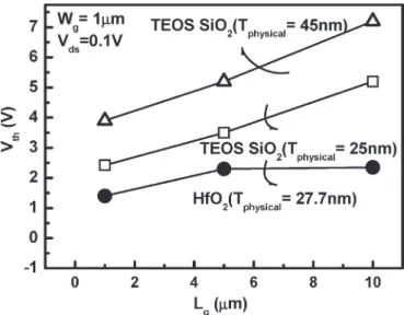
Fig. 4. Threshold-voltage rolloff of poly-Si TFTs with HfO2(Tphysical= 27.7 nm) and SiO2(Tphysical= 25 or 45 nm) at Vds= 0.1 V.
and Ion/Ioff increased from 5.4 × 10⁶ to 9.7 × 10⁶. The
gate-leakage current density of HfO2TFTs is about 1 µA/cm2
at Vgs= 5 V and is lower than that of SiO2 TFTs by more
than two times. The high gate capacitance density resulted from the high-κ gate dielectric could effectively improve the performance of HfO2 TFTs. Moreover, for devices with the
same EOT, the drawback of high gate-leakage current density of HfO2devices could be improved more effectively than that
of SiO2ones because of the thicker physical thickness of HfO2
[17], [18]. The EOT of HfO2TFTs atON-state is only 7.3 nm.
Possible reasons for the slightly low-κ value of 20.4 are the poly-Si gate depletion owing to the low activation tempera-ture and the interfacial layer between HfO2 and Si channel
[19], [20]. The slightly lower effective mobility of HfO2TFTs
may be due to the additional scattering from HfO2 dielectric.
TheOFF-state current of the HfO2TFTs increases more rapidly
than that of the SiO2 TFTs as the gate voltage decreases
continuously. This phenomenon is explained by the higher electric field near the drain side due to thinner EOT of the HfO2
TFTs. It could be relaxed by lightly doped drain (LDD) or gate overlapped lightly doped drain (GOLDD) structures [21], [22]. To examine the short-channel effect of TFTs with different gate dielectrics, the threshold-voltages (Vth) rolloff of HfO2
and SiO2 TFTs are compared in Fig. 4. For poly-Si TFTs,
the threshold-voltage rolloff is dominated by the decreasing of number of grain boundary as the devices scale down [23]. For the long-channel poly-Si TFTs, the large number of grain boundaries in the channel raises the threshold voltage and degrades the effective mobility [24]. The HfO2TFTs with
ultra-thin EOT and large gate capacitance density can speedily fill the trap states at grain boundary and turn on the devices fast; therefore, not only release the grain-boundary effect but also lower the threshold voltage effectively.
IV. CONCLUSION
High-performance TFTs with HfO2as gate dielectric, which
provide thin EOT and high gate capacitance density are demon-strated for the first time. Compared to the TFTs with SiO2
as gate dielectric, the electrical characteristics including the threshold voltage, subthreshold swing, ON/OFF current ratio, carrier mobility, as well as Vthrolloff are effectively improved.
These results suggest that HfO2is a good candidate to serve as
a gate-dielectric material for high-performance poly-Si TFTs. REFERENCES
[1] T. Nishibe, “Low-temperature poly-Si TFTs by excimer laser annealing,” in Proc. Mater. Res. Soc. Symp., 2001, vol. 685E, pp. D6.1.1–D6.1.5. [2] B.-D. Choi, H.-S. Jang, O.-K. Kwon, H.-G. Kim, and M.-J. Soh,
“De-sign of poly-Si TFT-LCD panel with integrated driver circuits for an HDTV/XGA projection system,” IEEE Trans. Consum. Electron., vol. 21, no. 3, pp. 100–103, Mar. 2000.
[3] J. K. Lee, J. B. Choi, S. M. Seo, C. W. Han, and H. S. Soh, “The application of tetraethoxysilane (TEOS) oxide to a-Si: H TFT’s as the gate insulator,” in Proc. SID Dig., 1998, vol. 29, pp. 439–442.
[4] A. Takami, A. Ishida, J. Tsutsumi, T. Nishibe, and N. Ibaraki, “Threshold voltage shift under the gate bias stress in low-temperature poly-silicon TFT with the thin gate oxide film,” in Proc. Int. Workshop AM-LCD, Tokyo, Japan, Jul. 2000, pp. 45–48.
[5] M. Y. Um, S.-K. Lee, and H. J. Kim, “Characterization of thin film transistor using Ta2O5gate dielectric,” in Proc. Int. Workshop AM-LCD, Tokyo, Japan, Jul. 1998, pp. 45–46.
[6] Z. Jin, H. S. Kwok, and M. Wong, “High-performance polycrystalline SiGe thin-film transistors using Al2O3gate insulators,” IEEE Electron Device Lett., vol. 19, no. 12, pp. 502–504, Dec. 1998.
[7] B. W. Busch, O. Pluchery, Y. J. Chabal, D. A. Muller, R. L. Opila, J. R. Kwo, and E. Garfunkel, “Materials characterization of alternative gate dielectrics,” MRS Bull., vol. 27, no. 3, pp. 206–211, Mar. 2002. [8] H. S. P. Wong, “Beyond the conventional transistor,” IBM J. Res.
Develop., vol. 46, no. 2/3, pp. 133–168, Mar./May 2002.
[9] C. Hobbs, H. Tseng, K. Reid, B. Taylor, L. Hebert, R. Garcia, R. Hegde, J. Grant, D. Gilmer, A. Franke, V. Dhandapani, M. Azrak, L. Prabhu, R. Rai, S. Bagchi, J. Conner, S. Backer, F. Dumbuya, B. Nguyen, and P. Tobin, “80 nm poly-Si gate CMOS with HfO2gate dielectric,” in IEDM Tech. Dig., 2001, pp. 651–654.
[10] Y. Kim, C. Lim, C. D. Young, K. Mathews, J. Barnett, B. Foran, A. Agarwal, G. A. Brown, G. Bersuker, P. Zeitzoff, M. Gardner, R. W. Murto, L. Larson, C. Metzner, S. Kher, and H. R. Huff, “Con-ventional poly-Si gate MOS-transistors with a novel, ultra-thin Hf-oxide layer,” in VLSI Symp. Tech. Dig., 2003, pp. 167–168.
[11] N. Yamauchi, J.-J. J. Hajjar, R. Reif, K. Nakazawa, and K. Tanaka, “Char-acteristics of narrow-channel polysilicon thin-film transistors,” IEEE Trans. Electron Devices, vol. 38, no. 8, pp. 1968–1969, Aug. 1991. [12] Y. C. Wu, C. Y. Chang, T. C. Chang, P. T. Liu, C. S. Chen, C. H. Tu,
H. W. Zen, Y. H. Tai, and S. M. Sze, “High performance and high relia-bility polysilicon thin-film transistors with multiple nano-wire channels,” in IEDM Tech. Dig., 2004, pp. 777–780.
[13] T. K. Kang, C. C. Wang, B. Y. Tsui, and Y. H. Li, “Selectivity investigation of HfO2to oxide using wet etching,” in Proc. Semicond. Manuf. Technol. Workshop, 2004, pp. 87–90.
[14] H. C. Cheng, F. S. Wang, and C. Y. Huang, “Effects of NH3plasma pas-sivation on n-channel polycrystalline silicon thin-film transistors,” IEEE Trans. Electron Devices, vol. 44, no. 1, pp. 64–68, Jan. 1997.
[15] J. R. Hauser and K. Ahmed, “Characterization of ultrathin oxides using electricalC−V and I−V measurements,” in Proc. AIP Conf. Charact. and Metrol. ULSI Technol., 1998, vol. 449, pp. 235–239.
[16] X. Garros, C. Leroux, D. Blin, J.-F. Damlencourt, A.-M. Papon, and G. Reimbold, “Investigation of HfO2dielectric stacks deposited by ALD with a mercury probe,” in Proc. Conf. Solid-State Device Res., 2002, pp. 411–414.
[17] B. H. Lee, L. Kang, W. J. Qi, R. Nieh, Y. Jeon, K. Onishi, and J. C. Lee, “Ultrathin hafnium oxide with low leakage and excellent reliability for alternative gate dielectric application,” in IEDM Tech. Dig., 1999, pp. 133–136.
[18] S. Datta, G. Dewey, M. Doczy, B. S. Doyle, B. Jin, J. Kavalieros, R. Kotlyar, M. Metz, N. Zelick, and R. Chau, “High mobility Si/SiGe strained channel MOS transistors with HfO2/TiN gate stack,” in IEDM Tech. Dig., 2003, pp. 653–656.
[19] J. J. Lee, J. S. Maa, D. J. Tweet, and S. T. Hsu, “Strain silicon thin film transistors fabricated on glass,” Appl. Phys. Lett., vol. 86, no. 3, pp. 103504.1–103504.3, 2005.
[20] Y. Kim, G. Gebara, M. Freiler, J. Barnett, D. Riley, J. Chen, K. Torres, J. Lim, B. Foran, F. Shaapur, A. Agaral, P. Lysaght, G. A. Brown,
LIN et al.: HIGH-PERFORMANCE POLY-SILICON TFTs USING HfO2GATE DIELECTRIC 363
C. Young, S. Borthakur, H.-J. Lin, B. Nguyen, P. Zeitzoff, G. Bersuker, D. Derro, R. Bergmann, R. W. Nurto, A. Hou, H. R. Huff, E. Shero, C. Pomarede, M. Givens, M. Mazanec, and C. Werkhoven, “Conven-tional n-channel MOSFET devices using single layer HfO2and ZrO2as high-κ gate dielectrics with polysilicon gate electrode,” in IEDM Tech. Dig., 2001, pp. 455–458.
[21] W. Y. So, K. J. Yoo, S. I. Park, H. D. Kim, B. H. Kim, and H. K. Chung, “Novel self-aligned LDD/offset structure for poly-Si thin film transistors,” in Proc. SID, 2001, pp. 1250–1253.
[22] K. Ohgata, Y. Mishima, and N. Sasaki, “A new dopant activation tech-nique for poly-Si TFTs with a self-aligned gate-overlapped LDD struc-ture,” in IEDM Tech. Dig., 2000, pp. 205–208.
[23] S. Chopra and R. S. Gupta, “An analytical model for current–voltage char-acteristics of a small-geometry poly-Si thin-film transistor,” Semicond. Sci. Technol., vol. 15, no. 11, pp. 1065–1070, Nov. 2000.
[24] A. G. Lewis, T. Y. Huang, I. W. Wu, R. H. Bruce, and A. Chiang, “Physical mechanisms for short channel effects in polysilicon thin film transistors,” in IEDM Tech. Dig., 1989, pp. 349–352.