國 立 交 通 大 學
電信工程學系
博 士 論 文
具精確頻寬之平行耦合微帶線帶通濾波器
合成方法
Synthesis of Parallel-Coupled Microstrip Bandpass
Filters with Accurate Bandwidths
研究生:金國生
(Kuo-Sheng Chin)
指導教授:郭仁財 博士
(Dr. Jen-Tsai Kuo)
具精確頻寬之平行耦合微帶線帶通濾波器
合成方法
Synthesis of Parallel-Coupled Microstrip
Bandpass Filters with Accurate Bandwidths
研究生: 金國生 (Kuo-Sheng Chin)
指導教授: 郭仁財 博士 (Dr. Jen-Tsai Kuo)
國 立 交 通 大 學
電 信 工 程 學 系
博 士 論 文
A Dissertation Submitted to
Department of Communication Engineering
College of Engineering
National Chiao Tung University
in Partial Fulfillment of the Requirements
in
Communication Engineering
July 2005
Hsinchu, Taiwan, Republic of China
中華民國 九十四 年 七 月
具精確頻寬之平行耦合微帶線帶通濾波器合成方法
研究生: 金國生
指導教授: 郭仁財 博士
國立交通大學 電信工程學系
摘要
在本論文,作者提出平行耦合微帶線帶通濾波器之新合成方法,可獲取精確 頻寬。傳統上,一段平行線耦合級係以兩段1/4 波長傳輸線及中間夾一個導納轉 換器來等效,由於導納轉換器並不具隨頻率改變之特性,因此此種等效模式僅在 設計小頻寬時較為準確,當設計較大頻寬時,實際頻寬會明顯大幅縮減。為改善 此問題,論文第一部份提出以頻帶邊緣等效取代中心頻率等效之觀念來修正傳統 公式,以獲取較為精確之頻寬。更進一步地,論文第二部份提出以介入損耗函數 來合成具有精確頻寬之平行耦合線帶通濾波器之方法。介入損耗函數可直接由耦 合級串接之 ABCD 矩陣推導得出,而不需使用含導納轉換器之等效電路,藉由 與最大平坦函數及柴比雪夫函數比對係數,得出所需之合成公式。由於在某些嚴 苛設計規格下,耦合線線寬及線距可能過窄難以實現,此時可運用合成公式提供 之自由度適當選擇解答,放寬中間耦合級之尺寸,將困難移至兩端(輸入及輸出 端)耦合級,並採用擇定饋入法(Tapped input)方式來實現端級。作者並實際合成 數組大頻寬濾波器作為範例,以模擬及量測數據來與本文之理論計算結果做比 較,證實此方法可行且頻寬相當精確。Synthesis of Parallel-Coupled Microstrip Bandpass Filters
with Accurate Bandwidths
Student: Kuo-Sheng Chin
Advisor: Dr. Jen-Tsai Kuo
Department of Communication Engineering
National Chiao Tung University
Abstract
In the thesis, authors propose the new synthesis methods of parallel-coupled microstrip bandpass filters (PCBPFs) with accurate bandwidth. In a conventional design, the equivalence of a coupled stage is established by using two quarter-wave transmission line sections with a J-inverter in between. Since the J-inverter is independent of frequency, the conventional equations are accurate only for filters with relatively narrow bandwidths. When a large bandwidth is designed, filters synthesized based on the conventional method will have a fractional bandwidth less than specification. In the first part of the dissertation, for recovering the bandwidth decrement, the correction θ = (π/2)(1 ± ∆/2) is incorporated into the synthesis formulas to modify the conventional method. Furthermore, the insertion loss (IL) functions are derived for synthesis of PCBPFs with accurate bandwidth. The synthesis is based on the composite ABCD matrix of all coupled stages instead of modeling each stage with the J-inverter equivalent circuit. Synthesis equations are established by matching the coefficients of IL function with the maximally-flat and Chebyshev functions. The under-determined conditions leave several degrees of freedom in choosing the circuit dimensions. By properly utilizing these degrees of freedom, the problem resulted from the tight coupled-line dimensions can be resolved by gathering all difficulties to the end stages and employing tapped input/output to replace the end stages. Several filters are
謝誌
「你或向左、或向右,你必聽見後邊有聲音說,這是正路,要行在其間。」 ─以賽亞書三十章二十一節 人的一生常常在等待一個適當時機,做出一個正確的決定,每個人都想走一 條自己的路… 四年前的某個深夜,我在中科院服務近十五年時,在決定報考博士班的剎 那,其實心情是相當猶疑的!考量的原因有許多;時間上只能以半工半讀的方式 攻讀,而孩子三、四歲年紀正需費心照顧,教會的服事重,且自己年近四十歲, 是否還有衝勁承受修課、作研究的壓力?而學位對我的未來又有何助益?未來會 走教職這條路嗎?...一念間決定的並不只是眼前四年光陰,更隱含著對未來的生 涯規劃。我站在人生關鍵的十字路口,思索著該往左或往右?腦海裡反覆想著各 種可能的組合,屋外漆黑的夜色逐漸被黎明的曙光染白… 四年修業時光轉眼即過,即使在研究、考試最不順心的時候也不曾後悔過, 一路行來,所有的甘苦只能自己體會,而我始終堅持著那晚的抉擇。如今仍清楚 記得作下決定剎那的心情,在我人生的轉折點上,勇敢堅定地,決心走出一條自 己的路。 關鍵的時刻感謝有許多關鍵的人幫助了我。特別要感謝我的指導教授─郭仁 財博士,他給了我學習及成長的空間,由他的身上我體會到學術研究努力不懈的 態度,每當遇到瓶頸時,他的指導總為我開啟一條出路,使我能順利完成論文。 謝謝諸位口試委員對論文內容的指正及建議。也要感謝實驗室夥伴們,一起研究 討論,並給予我許多協助,這些回憶都深植腦海。感謝中科院五所高溫材料組長 官及同仁對我的鼓勵與包容。感謝石門浸信會弟兄姊妹的代禱。 感謝自小為我操勞的雙親,在高齡九十及八十三歲的晚年仍要為我求學之路 掛心,他倆的支持成為我最大的動力來源。感謝兄姊們的愛護,尤其是我的大姊, 為我擔起照顧雙親的重責。最感謝的是我的妻子-林美,她全程陪我走過博士求 學的路程,不論是研究受挫的苦悶抱怨,或是論文被接受的興奮喜悅,都和她一 起承擔分享。當然還有我的寶貝兒子-小羽、小杰,謝謝你們給我無盡的愛。 要感謝的人太多,願將一切感謝歸給上帝,在我分不清或左或右時,祂總帶 領我平安度過。 金國生 於交大 民國九十四年七月Contents
Abstract (Chinese)…..………..I Abstract (English)………..………..………II Acknowledgements……….III Contents………...………...IV List of Tables……...……….…...…VI List of Figures…...………..………...VII Chapter 1 Introduction……….……...11-1 New Formulas for Synthesizing Microstrip Bandpass Filters with Relatively Wide Bandwidths……..………..…………..………...1
1-2Insertion Loss Function Synthesis of Maximally Flat Parallel-Coupled Line Bandpass Filters……..……….2
1-3 Direct Synthesis of Parallel-Coupled Line Bandpass Filters with Chebyshev Responses…...………..3
Chapter 2 New Formulas for Synthesizing Microstrip Bandpass Filters with Relatively Wide Bandwidths……….……….……..5
2-1 Design Formulas with Improved Accuracy………..…………6
2-2 Filter Fabrication and Measurements………..…….……....9
Chapter 3 Insertion Loss Function Synthesis of Maximally Flat Parallel-Coupled Line Bandpass Filters……..……….……….……..….15
3-1 The Maximally Flat Insertion Loss Function…………..……….………..16
3-1-1 First-Order Filters………..……...………...……..…...19
3-1-2 Third-Order Filters………...…...…....19
3-1-3 Fifth-Order Filters……….……….………...21
3-2 Three Examples………..…………..…..26
3-2-1 Filter α………..26
3-2-2 Filter χ ………....……30
3-2-3 Filter β………...………....35
3-3 Implementation Using Tapped Input/Output………….……….…....…...37
3-3-1 Filter δ……….……...38
3-3-2 Filter γ………....…...42
Chapter 4 Direct Synthesis of Parallel-Coupled Line Bandpass Filters with Chebyshev Responses……...………..………...44
4-1 The Chebyshev Insertion Loss Function………….………...…....45
4-1-1 Second-Order Filters…...……….….……...……...46
4-1-2 Filters of Order N ≤ 5……….…....……….…...…...48
4-2 The Ripple Level and Bandwidth……….…..…….….……..51
4-2-1 Ripple Level Specified by θm………….………..…...51
4-2-2 Ripple Level Specified by θd………...……...….…..……...52
4-3 Three Examples………….……….…...……57 4-3-1 Filter η (N = 3, ∆ = 50%, R = 0.5dB)………57 4-3-2 Filter ξ (N = 4, ∆ = 40%, R = 0.1dB)………....64 4-3-3 Filter ψ (N = 5, ∆ = 40%, R = 0.1dB)………...69 Chapter 5 Conclusion……….…..…..72 Reference……….……....74
List of Tables
Table 2.1 Even and Odd Mode Characteristic Impedances for the nth Coupled Stages
of an Nth-order Chebyshev Filter Obtained by the Improved and Classical Formulas. Ripple Level = 0.1dB and ∆= 50%....……….…9
Table 3.1 The Maximally Flat Conditions for N = 1 ~ 6.……….……..23
Table 3.2 The Chosen Solutions and Modal Characteristic Impedances of Each Coupled Stage of Filters α, χ and β……….……..………27 Table 3.3 The Chosen Roots and Modal Impedances of the Two Experimental Filters
with Tapped Inputs……….………41
Table 4.1 The Chebyshev Conditions for N = 1 ~ 5.………...…...50
Table 4.2 The Influences of Using θd on Ripple Level Design of Third-order Filters………..56
Table 4.3 The Chosen Roots and Modal Impedances of The Three Experimental Filters with Tapped Inputs………..63
List of Figures
Figure 2.10 (a) A coupled-line stage. (b) Equivalent circuit of (a).…..……….….…6
Figure 2.2 Normalized characteristic impedances Zoe and Zoo versus designed
bandwidths with ripple level 0.1dB. (a) N = 3. (b) N = 5.………..10
Figure 2.3 Bandwidth decrement versus designed bandwidth from simulation responses of a third- and fifth-order Chebyshev filters with 0.1dB ripple level.………...………...…...12
Figure 2.4 Comparison of responses for third-order filters designed by the improved and classical formulas. The designed bandwidth is 50% and ripple level is 0.1dB. The substrate has εr = 10.2 and thickness d = 1.27mm………...13 Figure 2.5 (a) Comparison of responses for fifth-order filters designed by the
improved and classical formulas. The designed bandwidth is 50% and ripple level is 0.1dB. The substrate has εr = 10.2 and thickness d = 1.27mm. (b) Photograph of the fifth-order filter.…………...………….14
Figure 3.1 An N-order parallel-coupled line filter.……….……….…..…..16
Figure 3.2 The ith coupled stage has line width Wi and gap Gi. Even and odd mode
characteristic impedances are respectively Zoei and Zooi.………….…....16
Figure 3.3 The calculated maximally flat responses of N =1, 3 and 5. Fractional bandwidth ∆ = 50%, fo = 5.8 GHz.………...25
Figure3.4 Possible roots for S2 and T2 with respect to T1 for a third-order filter with
∆ = 30% and ∆ = 50%.………...………..…...27
Figure 3.5 Root loci for Zoe and Zoo of the first and second stages of filter α when Zo
= 50 Ω and 90 Ω.……….……28
Figure 3.6 (a) Theoretical and measured responses of filter α. (b) Photograph of the fabricated circuit. fo = 5.8GHz, N = 3 and ∆ = 30%. Circuit dimensions:
W1 = 0.24 mm, G1 = 0.15 mm, W2 = 1.45 mm, G2 = 0.13 mm. The line
width of the quarter-wave transformer is 0.8mm. Substrate: εr = 10.2, thickness = 1.27 mm………..…..…...29
Figure 3.7 Possible roots for the 2nd and 3rd coupled stages of the fifth-order filter with ∆ = 40%.……….…...32
Figure 3.8 Root loci for Zoe and Zoo of the first, second and third stages of the
fifth-order filter with ∆ = 40% and Zo = 50 Ω.……..………...33
Figure 3.9 Simulated and theoretical responses of the synthesized filter χ. fo =
5.8GHz, N = 5, ∆ = 40%. Circuit dimensions: W1 = 0.767 mm, G1 = 0.001
mm, W2 = 1.94 mm, G2 = 0.005 mm, W3 = 2.1 mm, G3 = 0.1 mm…..…34
Figure 3.10 Root loci of S3, T3, S4 and T4 for a sixth-order filter with ∆ = 30% for (S2,
T2) = (0.49, 0.28), (0.96, 0.51) and (1.54, 0.61)………..36
Figure 3.11 Simulation and theoretical responses of filter β. fo = 5.8GHz, N = 6, ∆ =
30%. Circuit dimensions: W1 = 0.24 mm, G1 = 0.06 mm, W2 = 1.27 mm,
G2 = 0.02 mm, W3 = 0.92 mm, G3 = 0.47 mm, W4 = 0.55 mm, G4 = 0.78
mm………..36
Figure 3.12 A tapped line treated as a two-port network.………..…………....39
Figure 3.13 Comparison of |S21| responses of tapped lines and coupled stages…….39
Figure 3.14 (a) Theoretical, simulated and measured responses of filter δ. fo = 5.8GHz,
N = 3, ∆ = 50%. (b) Photograph of the fabricated circuit. Circuit dimensions: W1 = 2mm, W2 = 0.54mm, G2 = 0.23mm.……….…..40
Figure 3.15 (a) Theoretical, simulated and measured responses of filter γ. fo = 5.8GHz,
N = 5, ∆ = 40%. (b) Photograph of the fabricated circuit. Circuit dimensions: W1 = 1.7mm, W2 = 0.58mm, W3 = 1.2mm, G2 = 0.22mm, G3 =
0.22mm………...43
Figure 4.1 Calculated Chebyshev responses with ripple levels specified by θm and θd. N = 2, R = 3dB, ∆ = 50%, fo = 5.8 GHz..………...………....54
Figure 4.2 Calculated responses of third-order Chebyshev filters, with ripple levels specified by θd. (a) With ripple level R = 0.5dB. (b) With designed bandwidth ∆ = 50% .………..……..………..…55
Figure 4.3 Detailed |S21| performance within passband of fourth-order filters with
with R = 0.5 dB and ∆ = 50%..………...……….………59 Figure 4.5 Root loci for Zoe and Zoo of the first and second stages of third-order filter
when Zo = 50 Ω..………...……….………...60
Figure 4.6 Comparison of |S21| responses of tapped lines and coupled stages…..…61
Figure 4.7 (a) Theoretical, simulated and measured responses of filter η. (b) Photograph of the fabricated circuit. fo = 5.8GHz, N = 3, ∆ = 50%, R =
0.5dB. Circuit dimensions: W1 = 2mm, W2 = 0.286mm, G2 = 0.206mm.
Substrate: εr = 10.2, thickness = 1.27 mm….………...……..62 Figure 4.8 Possible roots for S2, T2, S3 and T3 with respect to T1 for a fourth-order
filter with R = 0.1dB and ∆ = 40%. (a) With k = 2. (b) With k = 1. (c) With k = 0.5....………...……….…….………65 Figure 4.9 Root loci for Zoe and Zoo of the second and third stages of a fourth-order
Chebyshev filter with k = 2, 1 and 0.5 when Zo = 50 Ω..………....67
Figure 4.10 (a) Theoretical, simulated and measured responses of filter ξ. fo = 5.8GHz,
N = 4, ∆ = 40%, R = 0.1dB. (b) Photograph of the fabricated circuit. Circuit dimensions: W1 = 2mm, W2 = 0.49mm, W3 = 0.41mm G2 =
0.23mm, G3 = 0.31mm..…..………...………….…68
Figure 4.11 Possible roots for the 2nd and 3rd coupled stages of a fifth-order parallel-coupled line filter with ∆ = 40%, R = 0.1dB and k = 0.5……...70
Figure 4.12 (a) Theoretical, simulated and measured responses of filter ψ. fo =
5.8GHz, N = 5, ∆ = 40%, R = 0.1dB. (b) Photograph of the fabricated circuit. Circuit dimensions: W1 = 1.97mm, W2 = 0.4mm, W3 = 0.16mm, G2
Chapter 1
Introduction
1-1 New formulas for synthesizing microstrip bandpass filters with relatively wide bandwidths:
The ultra-wideband (UWB) technologies for commercial communication applications have created a need of a transmitter with bandwidths of up to or more than several GHz [1]. Microwave passive devices with such a wide bandwidth have been investigated recently [2–4]. Lumped elements are incorporated into the circuit design for a directional coupler with an octave-band [2]. The three-line structures in [3] and ground plane aperture compensation techniques in [4] are suitable for implementing filters of a wide bandwidth.
Consisting of a cascade of coupled stages, parallel-coupled line configuration is attractive for realizing microstrip bandpass filters in microwave frequencies [3-7]. It is popular since it has an easy synthesis procedure and a wide range of realizable bandwidths. In a conventional design, approximate synthesis formulas have been well documented for determining dimensions of each coupled stage [6-7]. In deriving these formulas, one of the key steps is to establish the equivalence of a coupled stage to a two-port network of two quarter-wave transmission line sections with an admittance inverter in between. The approximation has a good accuracy when the filter has a relatively small bandwidth. This is because the frequency response of a coupled stage has a zero derivative at center frequency fo, and thus is relatively insensitive to
frequency moves away from fo. Thus, a modification is required for the formulas when
the microstrip filters are designed to have a wide bandwidth.
In Chapter 2, simple formulas are proposed for improving prediction of the bandwidth of parallel-coupled microstrip filters. Two experimental Chebyshev filters are measured to demonstrate the significant improvement.
1-2 Insertion loss function synthesis of maximally flat parallel-coupled line bandpass filters:
As mentioned in Section 1-1, since the admittance inverter in equivalent circuit is assumed independent of frequency, the conventional formulas are accurate only for bandpass filters (BPFs) with a relative small bandwidth (BW).
BPFs synthesized based on the conventional method will have a fractional BW ∆
less than specification. The BW decrement deteriorates as filter order or designed BW is increased. As reported in [13], when filter order N = 3 and ∆ = 35%, the synthesized
circuit has only ∆ = 30%. When ∆ = 50%, the realized BWs are only 41% and 38% for N = 3 and N = 5, respectively. For recovering the BW decrement, new formulas for determining Zoe and Zoo of each coupled stage have been derived in Chapter 2 for
synthesizing relatively wideband filters. In this way, the realized BWs can be greatly improved, but the BW decrement is still not completely resolved. For example, when ∆
= 50% is given, the new designs still have only 48.2% and 44% for N = 3 and N = 5, respectively.
Some methods have been proposed to design filters with accurate passband responses. In [14], insertion loss (IL) functions are derived for maximally flat filters with short- circuited quarter-wave stubs. The Q distribution method in [8] can provide accurate solutions to filters with narrow and wide BWs. Entire procedure for finding
the Q distribution includes choosing the number of sections, creating composite ABCD matrix, and solving individual admittance values of the resonators. For direct-coupled microwave filters of 2 ~ 12 resonant elements having ∆ = 10% ~ 43%, the theoretical
results in [9] have good agreement with computed responses. In [38], the synthesis formulas are derived based on the image parameter method and the insertion loss method, which are available for the design of wide-band and narrow-band microwave filters.
In Chapter 3, the IL function of a parallel-coupled bandpass filter is derived for synthesizing maximally flat responses. The synthesis formulas are derived directly from the composite ABCD matrix of all coupled stages instead of using J-inverter equivalent circuits. Based on the derived function, simultaneous conditions for determining dimensions of all coupled stages are provided. Section 3-1 shows the derivation for filters of order N ≤ 6. Section 3-2 presents results of three filters to demonstrate the formulation and synthesis. In realizing two additional relatively wideband filters, pattern resolution of certain stages exceeds our fabrication limits. Thus in Section 3-3 tapped lines are designed to resolve this problem. Measured responses are compared with EM simulation and theoretical predictions.
1-3 Direct synthesis of parallel-coupled line bandpass filters with Chebyshev responses:
The formulation in Chapter 3, however, is limited to maximally flat responses. Chebyshev filters can have more applications than those of the maximally flat type, due to the degree of freedom in trade-off between the ripple level in passband and rejection rate in transition band. Chapter 4 extends the method developed in Chapter 3 to
order N ≤ 5, and Section 4-2 investigates the performance of synthesized responses associated with given ripple level and BW. The IL functions can not give absolute equal ripples when N ≥ 4. A viable method is provided to improve the situation. Section 4-3 presents three filters to demonstrate the formulation and synthesis. Measured responses are compared with theoretical predictions as well as the simulated obtained by an EM software package.
Chapter 2
New Formulas for Synthesizing Microstrip
Bandpass Filters with Relatively Wide
Bandwidths
Approximate design equations for each coupled stage in a parallel-coupled microstrip filter have been given by [6-7] and adopted popularly in realization. The classical design formulas for determining the dimensions of each coupled stage are derived based on an assumption that the admittance inverter is independent of frequency. As a result, these equations are accurate only for filters with relatively narrow bandwidths. Thus, for parallel-coupled microstrip filters designed to have a wide bandwidth, the design formulas need modifying.
New formulas are proposed for designing wideband parallel-coupled microstrip bandpass filters with improved prediction of bandwidth. When a fractional bandwidth ∆ is required, a correction θ = (π/2)(1 ± ∆/2) is incorporated into the formulation for determining the dimensions of each coupled stage. Two filters with ∆ = 50% are
designed and fabricated to show the improvement. The measurement shows a very good agreement with the simulation.
2-1 Design Formulas with Improved Accuracy
From the perspective of circuit synthesis, accurate dimensions of the coupled stage are the most important in implementing the filter. The coupled stage in Fig. 2.1(a) has an electrical length θ, and even and odd mode characteristic impedances Zoe and
Zoo.
The impedance matrix elements of the coupled stage in Fig. 2.1(a) can be derived [7] as
(
)
cotθ 2 22 11 Zoe Zoo j Z Z = =− + (2.1a)(
)
cscθ 2 21 12 Zoe Zoo j Z Z = = − − (2.1b)Z , Z
oe oo0
(a)J
Z
oZ
o0
0
(b)Here, the even- and odd-mode phase velocities for the coupled stage are assumed identical. From (2.1a) and (2.1b), the ABCD matrix for the coupled-line stage can be derived as
(
)
⎥ ⎥ ⎥ ⎥ ⎦ ⎤ ⎢ ⎢ ⎢ ⎢ ⎣ ⎡ − + − ⎭ ⎬ ⎫ ⎩ ⎨ ⎧ − − − − + = ⎥⎦ ⎤ ⎢⎣ ⎡ θ θ θ θ θ θ cos sin 2 sin cos 4 sin 2 cos 2 oo oe oo oe oo oe oo oe oo oe oo oe oo oe oo oe Z Z Z Z Z Z j Z Z Z Z Z Z j Z Z Z Z D CA B (2.2)The ABCD matrix for the J inverter circuit in Fig. 2.1(b) can be derived as
⎥ ⎥ ⎥ ⎥ ⎥ ⎦ ⎤ ⎢ ⎢ ⎢ ⎢ ⎢ ⎣ ⎡ ⎟⎟ ⎠ ⎞ ⎜⎜ ⎝ ⎛ + ⎟⎟ ⎠ ⎞ ⎜⎜ ⎝ ⎛ − ⎟⎟ ⎠ ⎞ ⎜⎜ ⎝ ⎛ − ⎟⎟ ⎠ ⎞ ⎜⎜ ⎝ ⎛ + = ⎥ ⎥ ⎦ ⎤ ⎢ ⎢ ⎣ ⎡ ⎥ ⎥ ⎦ ⎤ ⎢ ⎢ ⎣ ⎡ − − ⎥ ⎥ ⎦ ⎤ ⎢ ⎢ ⎣ ⎡ = ⎥⎦ ⎤ ⎢⎣ ⎡ θ θ θ θ θ θ θ θ θ θ θ θ θ θ θ θ sin cos 1 cos sin 1 cos sin sin cos 1 cos sin sin cos 0 0 cos sin sin cos 2 2 2 2 2 2 o o o o o o o o o o JZ JZ J JZ j J JZ j JZ JZ Z j jZ jJ J j Z j jZ D CA B (2.3)
Equating the right hand sides of (2.2) and (2.3), one can express Zoe and Zoo in terms of
the circuit parameters of the admittance inverter as follows
] 1 sin ) 1 [( ) cos ( sin sin 2 2 2 + + − = θ θ θ θ o o o o oe JZ JZ JZ JZ Z (2.4a) ] 1 sin ) 1 [( ) cos ( sin sin 2 2 2 − + − =
θ
θ
θ
θ
o o o o oo JZ JZ JZ JZ Z (2.4b)It is difficult to implement a coupled microstrip stage having a frequency-dependent behavior as described in (2.4). In fact, constant values for Zoe and
Zoo have to be used to determine the dimensions of each stage from the characteristic
impedance design graphs. Note that if θ = π/2 is used, (2.4a) and (2.4b) reduce to those given in [7]. Since the approximation θ = π/2 is accurate only in the vicinity of the center frequency, this may lead to an error in estimating the filter bandwidth. Thus, when the required fractional bandwidth is ∆,
(1
)
2
2
π
θ
=
±
∆
(2.5)can be used to calculate the Zoe and Zoo for each coupled stage. Obviously, an exact
equivalence between the circuits in Fig. 2.1(a) and Fig. 2.1(b) is assured at the passband edges. This will make the prediction of filter bandwidths more accurate, which will be demonstrated later.
2-2 Filter Fabrication and Measurements
To show the significant improvement in predicting the filter bandwidth provided by (2.4) and (2.5), we first examine the changes of Zoe and Zoo of coupled microstrip
stages due to the deviation of θ from π/2. Table 2.1 lists their values for the nth coupled
stage in a third-, a fifth- and a seventh-order Chebyshev filters with 0.1dB ripple level and 50% fractional bandwidth.
It is noted that for an Nth-order Chebyshev filter, the nth coupled stage is identical to the (N+2-n)th one. The numbers in Table 2.1 indicate that the end stages have the largest change in Zoo, which is increased by no more than 6% for all cases shown here.
On the other hand, the value of Zoe exhibits a significant change; for example, Zoe is
increased by more than 20Ω for the end stages.
TABLE 2.1
EVEN AND ODD MODE CHARACTERISTIC IMPEDANCES FOR THE nthCOUPLED STAGES OF AN NTH-ORDER
CHEBYSHEV FILTER OBTAINED BY THE IMPROVED AND CLASSICAL FORMULAS. RIPPLE LEVEL =0.1dB AND ∆=50%.
N Improved Classical n Zoe(Ω) Zoo(Ω) Zoe(Ω) Zoo(Ω) 3 1 155.6 47.0 131.7 44.4 2 126.4 40.6 112.2 40.0 1 146.2 44.7 125.6 42.9 5 2 111.0 38.3 100.9 38.3 3 90.8 37.0 85.3 37.5 1 143.8 44.2 124.0 42.5 2 107.9 38.0 98.6 38.1 3 88.1 37.0 83.1 37.6 4 85.5 37.1 81.0 37.7 7
Fractional Bandwidth Δ(%)
Normalized
Characteristic I
m
pedance
1.8
1.7
1.6
1.5
1.4
1.3
1.2
1.1
1.0
0.9
20
30
40
50
60
70
1st Z
oe' / Z
oe1st Z
oo' / Z
oo2nd Z
oe' / Z
oe2nd Z
oo' / Z
oo (a)0.9
1.0
1.1
1.2
1.3
1.4
1.5
1.6
1.7
1.8
20
30
40
50
60
70
Fractional Bandwidth Δ(%)
1st Z
oe' / Z
oe1st Z
oo' / Z
oo2nd Z
oe' / Z
oe2nd Z
oo' / Z
oo3rd Z
oe' / Z
oe3rd Z
oo' / Z
ooNormalized
Characteristic Impedance
(b)
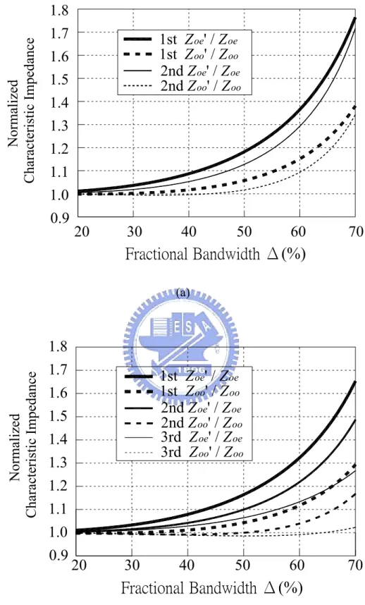
Figure 2.2 Normalized characteristic impedances Zoe and Zoo versus designed bandwidths with ripple
Fig. 2.2(a) and 2.2(b) show the variations of normalized characteristic impedance Zoe and Zoo versus designed bandwidths with Chebyshev response, ripple level 0.1dB,
N = 3 and N = 5, respectively. The results are obtained by using the approximation condition (2.5). As shown in the figures, the normalized impedance Zoe of each coupled
stage is increased by the improved formulas, thus increased the coupling factor. The largest variation of normalized Zoe is occurred at the end stage.
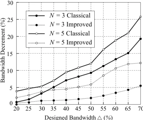
Next, we proceed to synthesize the parallel-coupled microstrip wideband filters. All the filters are designed on an RT/duroid 6010 substrate with εr = 10.2 and thickness d = 1.27mm. Fig. 2.3 plots the bandwidth decrement against the designed specification. The test vehicle includes a third- and a fifth-order Chebyshev filters of ripple level 0.1dB. In simulation by the full-wave simulator IE3D [10], the responses are obtained by discretizing the circuits with twenty and forty cells per wavelength, and they are found indistinguishable.
In Fig. 2.3, the curves denoted by “classical” are of filters obtained by (2.4) with θ = π/2, and those by “improved” are of filters synthesized by (2.4) and (2.5). When the filter order N = 3 and the designed bandwidth is less than 25%, the bandwidth decrement is insignificant. If ∆ is increased to 35%, however, the classical formulas
produce a fractional bandwidth with 5% less than the specification. The bandwidth decrement deteriorates as the filter order or the designed ∆ is increased. Upon the requirement of ∆ = 70%, in the classical design, the bandwidth decrements are close to
19% and 25% for N = 3 and N = 5, respectively, while in our proposed equations, the decrements are only about 5% and 12.5%.
Bandwidth Decrement ( % )
N = 3 Improved
N = 5 Classical
Designed Bandwidth (%) 20 25 30 35 40 45 50 55 60 65 70 0N = 3 Classical
N = 5 Improved
5 10 15 20 25 30Fig. 2.3 Bandwidth decrement versus designed bandwidth from simulation responses of a third- and fifth-order Chebyshev filters with 0.1dB ripple level.
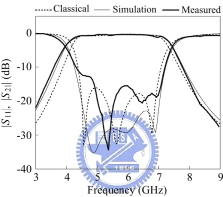
Finally, we examine the quality of the passband responses for filters designed with (2.4) and (2.5). Fig. 2.4 plots the simulation and measured responses for a third-order Chebyshev filter, and they show a very good agreement. Detailed data show that the simulated and measured results have fractional bandwidths of 48.4% and 48.2%, respectively, which are close to the designed bandwidth 50%. The measured results of a filter designed by classical formulas are also plotted for comparison. Its fractional bandwidth is only 41%.
Fig. 2.5(a) plots the results for a fifth-order filter. Again, the simulation and measured responses have a good agreement, and fractional bandwidths of 44.4% and 44%, respectively. For the filter based on the classical design, the measured response shows ∆ = 38%.
3
-40
-30
-20
-10
0
4
5
6
7
8
9
Frequency (GHz)
11|S
|,
21|S
| (
dB)
Simulation Classical MeasuredFig. 2.4 Comparison of responses for third-order filters designed by the improved and classical formulas. The designed bandwidth is 50% and ripple level is 0.1dB. The substrate has εr = 10.2 and thickness d =
3
-40
-30
-20
-10
0
4
5
6
7
8
9
Frequency (GHz)
Classical
Simulation
Measured
11
|S
|,
21|S
| (dB)
(a) (b)Fig. 2.5 (a) Comparison of responses for fifth-order filters designed by the improved and classical formulas. The designed bandwidth is 50% and ripple level is 0.1dB. The substrate has εr = 10.2 and
Chapter 3
Insertion Loss Function Synthesis of
Maximally Flat Parallel-Coupled Line
Bandpass Filters
Insertion loss (IL) functions are derived for synthesis of microstrip parallel-coupled line bandpass filters with maximally flat responses. The derivation is performed by successively multiplying the ABCD matrices of all coupled stages instead of using J-inverter equivalent circuits. Simultaneous equations for determining line width and line spacing of the coupled stages are established by total Q (QT) of the
filter specification and comparing the IL function with the canonical form. The results are provided for filters of order N ≤ 6. Two filters with fractional bandwidths ∆ = 30%
and a filter with ∆ = 40% are synthesized and demonstrated by simulation using an EM full-wave software package, while measurements are further performed for one of them. The results show very accurate bandwidths. The under-determined conditions leave several degrees of freedom in choosing the circuit dimensions. By properly utilizing these degrees of freedom, the problem resulted from the tight coupled-line dimensions can be resolved by gathering all difficulties to the end stages and employing tapped input/output to replace the end stages. Two filters with ∆ = 40% and
50% are fabricated to proof the feasibility. The measured results show very good agreement with the theoretical responses.
3-1 The Maximally Flat Insertion Loss Function
For the N-order parallel-coupled microstrip filter in Fig. 3.1, let the generator and load impedances be identical and normalized to unity. Since a maximally flat response is assumed, the circuit layout is symmetric about its center and, when it is characterized by a composite ABCD matrix, A = D holds. It can be shown that the IL function can be written as [6] 2 2 1 ( ) ] 2 ) ( [ 1 N L o j B C P P Ω + = − + = (3.1)
where j = −1, N is order, Po is power available from source, and PL is power delivered
to load.
1
2
N
N +1
Fig. 3.1 An N-order parallel-coupled line filter.
θ
oei ooi
Wi
Gi Z ,Z
Fig. 3.2 The ith coupled stage has line width Wi and gap Gi. Even and odd mode characteristic
Of an Nth-order filter, the impedance matrix elements of the ith coupled stage in Fig. 3.2 can be derived [7] as
(
)
cotθ 2 22 11i i Zoei Zooi j Z Z = =− + (3.2a)(
)
cscθ 2 21 12i i Zoei Zooi j Z Z = =− − (3.2b)where θ is its electrical length and Zoei and Zooi are the characteristic impedances of the
even- and odd-modes, respectively. Here, the even- and odd-mode phase velocities for all coupled stages are assumed identical. From (3.2a) and (3.2b), the ABCD matrix can be obtained as
[
]
⎥ ⎥ ⎦ ⎤ ⎢ ⎢ ⎣ ⎡ + − = ⎥ ⎦ ⎤ ⎢ ⎣ ⎡ i i i i i i i i i i qS j S T q T j qS T D C B A 2 ) ( 2 sinθ 2 2 2 2 (3.3a) q = cotθ (3.3b) o ooi oei i Z Z Z S = + (3.3c) o ooi oei i Z Z Z T = − (3.3d)The composite ABCD matrix of an N-order filter can be obtained by successively multiplying the N+1 ABCD matrices as follows:
⎥ (3.4) ⎦ ⎤ ⎢ ⎣ ⎡ ⎥ ⎦ ⎤ ⎢ ⎣ ⎡ ⎥ ⎦ ⎤ ⎢ ⎣ ⎡ = ⎥ ⎦ ⎤ ⎢ ⎣ ⎡ + + + + 1 1 1 1 2 2 2 2 1 1 1 1 N N N N N C D B A D C B A D C B A D C B A L
As N becomes large, the result of (3.4) can be very tedious and complicated. If the matrix entries are expressed in terms of q, however, the results become much simpler. Substituting (3.3a) for all stages into (3.4) yields
⎥ ⎦ ⎤ ⎢ ⎣ ⎡ × = ⎥ ⎦ ⎤ ⎢ ⎣ ⎡ + + ) ( ) ( ) ( ) ( ... sin 1 2 1 1 q f q f q f q f T T T D C B A d c b a N N N θ (3.5a) Where
[
]
[
]
⎥⎥ ⎦ ⎤ ⎢ ⎢ ⎣ ⎡ + + + + + + + + + + + + = ⎥ ⎦ ⎤ ⎢ ⎣ ⎡ + + + + + + 1 1 2 2 0 3 3 1 2 2 3 3 1 1 1 2 2 0 ... ... 2 ... 2 ... ) ( ) ( ) ( ) ( N N N N N N N N d c b a d q d q d c q c q qc j b q b q qb j a q a q a q f q f q f q f (3.5b)when N is odd, and
[
]
[
]
⎥⎥ ⎦ ⎤ ⎢ ⎢ ⎣ ⎡ + + + + + + + + + + + + = ⎥ ⎦ ⎤ ⎢ ⎣ ⎡ + + + + + + 1 1 3 3 1 2 2 0 2 2 2 2 0 1 1 3 3 1 ... ... 2 ... 2 ... ) ( ) ( ) ( ) ( N N N N N N N N d c b a d q d q qd c q c q c j b q b q b j a q a q qa q f q f q f q f (3.5c)when N is even. The coefficients of each polynomial are functions of Si and Ti. The
object of (3.5) is to find conditions for determining Zoei and Zooi, and hence geometries
3-1-1 First-order Filters:
When N = 1, the composite ABCD matrix is a product of two identical ABCD matrices. It can be derived that
⎥⎦ ⎤ ⎢⎣ ⎡ − + − = − ) ( 2 sin cos ) 2 1 2 ( cos sin 1 2 ) ( 2 1 2 1 1 3 1 1 2 1 T S S S S T C B j θ θ θ θ (3.6)
Comparing (3.6) with the canonical form (3.1), we have
2 or 0 2 1 2S1 − S13 = S1 = (3.7)
Substituting (3.7) into (3.6) yields the IL function
2 2 1 2 1 2 1 1 2 2 ) ( sin cos 1 ⎥ ⎦ ⎤ ⎢ ⎣ ⎡ − ⎥⎦ ⎤ ⎢⎣ ⎡ + = T T S S P P L o θ θ (3.8)
The condition for solving T1 can be obtained by imposing the given 3-dB bandwidth to
(3.8). This will be addressed later.
3-1-2 Third-order Filters:
For a third-order filter, S1 = S4, S2 = S3, T1 = T4, and T2 = T3. The composite ABCD
interchanged. The result can be written as )] ( sin cos ) ( cos sin ) ( cos [sin 2 1 2 ) ( 3 3 3 1 2 3 1 2 2 2 1 h h h h h T T C B j θ θ θ θ θ θ + − − + − = − (3.9a) Where ) ( ) ( 4 2 1 2 2 2 1 2 1 2 1 2 2 1 T S S T ST S T h = + − + (3.9b) ) 4 4 4 2 ( ) ( ) ( 2 2 1 2 2 2 2 2 1 2 1 2 1 2 2 2 1 2 1 2 2 2 1 2 1 2 S S S T S S T S T S S T S T S T h − − + + × + + + − = (3.9c) ] )[ ( ) ( ) ( 3 1 2 1 1 2 2 1 2 2 2 2 2 2 1 2 1 2 2 2 1 2 1 2 1 3 S T S S S S T S T S S S S T h + − − + − − − = (3.9d)
Matching (3.9a) with the canonical form (3.1), we reserve only the cos3θ/sinθ term, i.e., enforce h1 = 0 and h2 = h3, to eliminate the dependence of the IL function on sinθcosθ
and sinθcos3θ. It leads to the following two conditions:
2 1= S (3.10a) ) ( ) ( 4 2 1 2 2 2 1 2 1 2 1 2 2 S S T ST ST T + = + (3.10b)
Inserting (3.10b) and (3.9d) into (3.9a) yields
2 2 2 2 1 2 1 2 1 2 1 2 2 3 2 ( )[( ) ] sin cos 1 ⎥ ⎦ ⎤ ⎢ ⎣ ⎡ + + − ⎥ ⎦ ⎤ ⎢ ⎣ ⎡ + = T T T S S S S S P P L o θ θ (3.11)
The variable S1 is purposely kept in (3.11) since it is useful in expressing the IL
function in a general form. Note that there are four unknowns to be determined by only three equations, i.e., (3.10a), (3.10b), and (3.11) from given BW. Thus we have one degree of freedom in choosing the circuit dimensions.
3-1-3 Fifth-order Filters:
When N = 5, from the circuit symmetry, S1 = S6, S2 = S5, S3 = S4, T1 = T6, T2 = T5
and T3 = T4. It can be derived that
)] ( sin cos ) ( cos sin ) 2 ( cos sin ) ( cos [sin 2 1 2 ) ( 4 5 4 3 2 1 5 1 2 3 1 2 3 2 2 2 1 g g g g g g g g T T T C B j θ θ θ θ θ θ θ θ + − + − + − + − = − (3.12a) where 4 2 3 3 2 2 3 4 1 2 1 2 1 1 2 3 2 2 1 T T [ST 4(S S )] T T (S S ) 4ST g = − + + + − (3.12b) ) 4 ( ) ( )] ( [ 4 ] ) ( ) )[( 4 ( )] 2 ( ) 2 ( )[ 4 ( ) 2 )( ( 4 ] ) ( 2 )[ ] 4 ) )[( ( 2 2 3 2 1 2 3 2 2 1 2 3 2 2 2 3 2 4 1 3 2 3 2 2 1 3 2 2 2 3 2 2 2 3 2 3 2 3 2 2 2 2 2 1 1 3 2 2 2 3 1 3 2 2 3 2 1 2 1 2 2 3 2 3 2 2 2 2 2 2 1 3 2 2 2 1 2 1 2 3 2 2 2 4 1 3 2 2 3 2 3 2 T S S T S S S S T S S T S S S S S S S T T S T T S T T S S S T S S S S T S S T T S T S S T T S S T S S T T T S T S S S T g − − + + − + + + − + − − + + + + − − + − − + + − + − + − = (12 (3.12c) (3.12d) )] ( 4 [ ) 4 ( ) ( ) ( ) ( 4 ) )( )( 4 ( ) )( ( ) )( ( 4 ) 2 )( 4 )( ( ) 2 )( 4 )( ( )] ( 4 ) 4 ( )[ ) 2 4 )( ( )] ( 2 ) 2 ( ) 2 ( )[ ( ] ) ( 2 )[ )( ( 3 2 2 3 2 2 2 3 3 2 2 1 2 3 2 2 1 3 2 2 2 1 2 3 2 2 2 3 2 3 2 2 1 2 2 2 1 2 3 1 2 3 2 2 2 3 2 2 1 2 2 2 2 3 1 3 2 2 1 2 3 2 3 2 1 3 2 2 1 2 2 2 1 3 2 2 2 3 2 2 3 2 1 2 3 2 2 1 2 3 2 2 2 3 2 2 1 3 2 3 2 2 2 3 1 3 2 2 3 2 1 2 1 2 1 2 2 1 3 2 2 1 2 3 2 3 2 1 2 1 3 S S T S T S S S S T S S S S S S T T S T S S T S T T S S T S T T S S T S T S S S T S T S S S S T S T S S S S S T S S S S S T T S S T S S S S S T S S T S S S S T S S S S T S S S T T S S S T S T S T g + − + + − + + − + − − − − − + − − + − − − + − − − + − − − + + − − + − − − + + + + + + − − + + − − = 2 1 2 1 2 2 2 3 2 2 2 1 2 2 2 1 2 3 2 2 2 3 2 2 ( ) ( ) )( ( ) )( ( ) )( )( 2 ( ) )( )( 2 ( ) ( ) ( ) ( 3 2 2 3 2 3 2 2 1 2 1 3 2 2 3 2 3 2 2 2 2 2 2 1 2 2 2 2 2 1 2 1 3 2 3 1 2 3 2 3 2 1 2 1 3 2 2 1 2 3 2 3 3 2 2 2 1 2 2 2 2 2 3 2 2 1 2 1 2 1 2 3 2 2 1 4 S S S T S T S S S T S T S S S T S T S S S S S T S T S S S S S T S S S S T S S S S T S S S g − − − − + + − − − − − + − − − + − − + − + − = (3.12e)
Matching (3.12a) with the canonical form (3.1), we reserve only the cos5θ/sinθ term, i.e., enforce g1 = 0, g2 = 2g1 and g1-g2+g3-g4 = 0 to eliminate the dependence of the IL
function on sinθcosθ, sinθcos3θ and sinθcos5θ. It leads to the following three conditions: 2 1 = S (3.13a)
[
( )]
[
( )]
4 2 2 3 1 2 2 1 2 3 2 1 2 2 3 2 1 2 3 2 2 T S S ST T T ST T S S T + + = + + (3.13b)[
( ) 2 2 ( )]
) ( 4 ) ( 8 2 1 1 2 3 3 1 2 2 3 2 3 2 1 2 1 2 2 1 2 3 2 1 3 2 2S S S T S S T T S S S T SS T S S S T + + + = + + + + (3.13c)Inserting (3.13b) and (3.13c) into (3.12a) yields the IL function as
2 2 3 2 2 2 1 2 1 2 1 2 3 2 2 1 3 2 5 2 ( )( ) [( ) ] sin cos 1 ⎥ ⎦ ⎤ ⎢ ⎣ ⎡ + + + − ⎥ ⎦ ⎤ ⎢ ⎣ ⎡ + = T T T T S S S S S S S P P L o θ θ (3.14)
Note that in (3.14) there are six unknowns, i.e., S1, S2, S3, T1, T2, and T3, to be
determined. When the circuit bandwidth is given, there are only four conditions including (3.13a) ~ (3.13c). It means that we have two degrees of freedom in choosing the circuit dimensions.
3-1-4 Insertion Loss Function of a Filter of Order N ≤ 6:
For an Nth-order filter, the IL function can be derived in a similar fashion. The simultaneous equations for solving Si and Ti are obtained by saving cosNθ/sinθ term and
enforcing coefficients for all other terms to zero. It is found that a general expression exists for the IL functions of order N ≤ 6:
[ ]
2 2 sin cos 1 N N L o K P P ⎥ ⎦ ⎤ ⎢ ⎣ ⎡ + =θ
θ
(3.15a) 1 2 1 1 1 1 2 1 1 1 ... ) ( ) ( + = − = + +∏
+ −∏
+ = N N i N i i i i i N T T T T S S S S K (3.15b)It is interesting to note that in the θ-dependent term of (3.15a), the numerator is cos2Nθ and denominator is sin2θ. The former reflects the fact that the leading 2N – 1 derivatives of (3.15a) with respect to θ are zero at fo, and the latter implies a
transmission zero existing at 2fo where θ = π. The zero relies on the assumption that all
coupled-line stages in the filter have only one phase velocity.
The simultaneous conditions for determining Si and Ti are listed in Table 3.1. It is
found that S1 = 2 for each N. Note that total number of unknowns for an N-order filter is
N+1 for odd N and N+2 for even N. As shown in Table 3.1, only [N/2] + 2 conditions are obtained, including the condition specified by the bandwidth. Here, [N/2] is an integer by truncating N/2. It can be seen that number of equations is less than that of unknowns when N ≥ 2. For example, when N = 6, eight variables have to be found for four of seven coupled stages. Three free dimensions exist since these variables are specified by only five equations. This under-determined feature is very helpful for circuit realization since both line width and gap size of coupled microstrips have resolution limits in fabrication. This will be discussed in Section 3-3.
TABLE3.1
THE MAXIMALLY FLAT CONDITIONS FOR N=1~6.
N Maximally Flat Conditions Degree of Freedom
1 S1=2 0 2 2 1 2 1 2 2 T T S = = 1 3 4 (2 ) ( 2) 1 2 2 2 1 2 1 2 1 2 2 1 T S T S T S S T S + = + = 1 4
[
2 ( ) ( )]
2[
( ) ( ) ( )]
2 2 2 1 1 2 3 3 2 1 2 2 2 3 2 2 1 2 1 2 3 2 2 1 2 1 3 3 2 1 2 2 1 S S S T S S S T S S T T S S T S S T T T T S + + + + + = + + + = = 2 5[
]
[
]
[
( ) 2 2 ( )]
) ( 4 ) ( 8 ) ( ) ( 4 2 2 1 1 2 3 3 1 2 2 3 2 3 2 1 2 1 2 2 1 2 3 2 1 3 2 2 3 2 2 1 2 2 1 2 3 2 1 2 2 3 2 1 2 3 2 2 1 S S S T S S T S S S T T S S T S S S T S S T T S T T T S S S T T S + + + + = + + + + + = + + = 2 6[
]
[
[
]
]
)] )( ( 2 ) )( ( 4 ) ( 2 ) )( ( [ )] ( ) ( 2 ) ( 2 )[ )( ( 4 ) ( 8 2 ) ( ) ( ) ( ) ( ) )( ( 2 ) ( ) ( 4 2 2 3 2 2 1 1 2 4 4 3 2 1 1 2 3 2 4 3 1 2 2 2 4 3 3 2 2 1 2 1 2 1 2 4 2 1 2 3 4 3 2 2 3 2 2 1 2 1 2 2 1 2 2 2 1 3 2 4 1 3 2 2 4 2 1 1 2 3 4 3 1 2 2 4 3 3 2 2 1 2 3 2 1 2 2 1 2 3 4 3 2 2 2 3 2 1 4 2 2 1 S S S S S T S S S S S T S S S T S S S S T T S S T S S T S S T S S S S S S T S T T S S T S S T . S S S T S S S T S S S S T T T S S T S S T T T T T S + + + + + + + + + + = + + + + + + + + − + + + + + + + + + + = + + + = = 3 6.8 5.8 4.8 0 0.05 0.1 N = 3 N = 5 N = 1 60 50 40 30 20 10 20 18 16 Insertion Loss (dB) 0 14 12 Frequency (GHz) 4 6 8 10 0 2Fig. 3.3 The calculated maximally flat responses of N =1, 3 and 5. Fractional bandwidth ∆ =50%, fo = 5.8
3-1-5 The QT Condition and the 3-dB Bandwidth:
For a maximally flat filter, the total Q (QT) and the 3-dB bandwidth is related by
1 2 0 ω ω ω − = T Q (3.16)
where ω0 is the design frequency, and ω1 and ω2 are the 3-dB cutoff frequencies
specified by 2 1 2 1, = ω ω o L P P (3.17)
Thus, the electrical length θ can be written in terms of QT as
⎟⎟ ⎠ ⎞ ⎜⎜ ⎝ ⎛ ± = T Q 2 1 1 2 2 1, π θ ω ω (3.18)
and KN in (3.15a) can be derived as
2 1 2 1 , , cos sin ω ω ω ω θ θ N N K = (3.19) This is called the QT condition herein. For demonstration, based on (3.15a) and (3.19),
Fig. 3.3 plots the calculated maximally flat responses for N = 1, 3 and 5 with ∆ = 50% and fo = 5.8GHz. The inserted frame shows the detailed passband performance.
The synthesis method can be applied to Chebyshev filters as well. For example, when N = 3, the expressions of h1, h2, and h3 in (3.9a) are then specified by constants
3-2 Three Examples
A third-order filter α and a sixth-order filter β are synthesized with ∆ = 30%, and the fifth-order filter χ is synthesized with ∆ = 40% for validating the formulation. The center frequency is fo = 5.8GHz. Simulated results by the IE3D [10] are presented for
three circuits, while measurements are further performed for filter α. 3-2-1 Filter α:
When N = 3, the QT condition (3.19) gives
2 2 2 1 3 2 1 2 2 2 cos sin ] ) 2 )[( 2 ( 2S S S T T T θ θ = − + + (3.20)
where (3.10a) is used and, from (3.18), θ = 1.3352 radian. Inserting (3.10b) into (3.20) yields 0 cos sin ) 2 ( 4 ) 2 ( 12 ) 2 ( 8 6 1 3 4 1 2 2 1 2 2 3 2 − + + + − = +S S T S T T θ θ (3.21)
There is one degree of freedom in finding the solution. Fig. 3.4 plots the solutions of S2
and T2 for T1 ranging from 0.9 to 1.3. Referring to (3.3c) and (3.3d), we have Zoei = (Si
+ Ti)×Zo/2 and Zooi = (Si − Ti)×Zo/2. Obviously, not all roots shown in Fig. 3.4 are
realizable using the standard microstrip technology. Realizable Zoei and Zooi depend on
structural parameters, and obviously Zo is the dominant factor. Suppose that the filters
are designed on a substrate with εr = 10.2 and thickness d = 1.27mm. According to resolution of our fabrication facilities, G/d and W/d must be no less than 0.1. When Zo =
50Ω and 90Ω, Zoe and Zoo for the first and second stages are plotted together with the
design graph in Fig. 3.5. As T1 is increased, values of Zoe1, Zoe2, and Zoo2 increase while
that of Zoo1 decreases. If Zo = 50Ω is used, the gap size G/d for stage 1 will be no larger
than 0.1. If both stages are required to have G/d ≥ 0.1, for Zo = 90Ω, value of T1 must be
between 1.03 and 1.06. Therefore, the solution is chosen as S1 = 2, T1 = 1.043, S2 =
0.895 and T2 = 0.336. The corresponding modal characteristic impedances are listed in
∆=50%
S
2 3 2.5 2.0 1.5 1.0 1.6 1.5 1.4 1.3 1.2 1.1 1.0 2 1S
, T
0T
0.9 2S
2T
2∆=30%
T
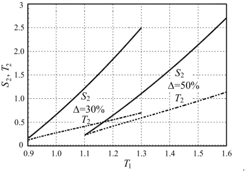
2 0.5 .Fig. 3.4 Possible roots for S2 and T2 with respect to T1 for a third-order filter with ∆ = 30% and ∆ = 50%.
TABLE 3.2
THE CHOSEN SOLUTIONS AND MODAL CHARACTERISTIC IMPEDANCES OF EACH COUPLED STAGE OF
FILTERS α,χ AND β
Filters 1st stage 2nd stage 3rd stage 4th stage
α N = 3 ∆ = 30% Zo = 90Ω S1 = 2 T1 = 1.043 Zoe1 = 136.93Ω Zoo1 = 43.07Ω S2 = 0.895 T2 = 0.336 Zoe2 = 55.40Ω Zoo2 = 25.16Ω Same as the 2nd stage Same as the 1st stage χ N = 5 ∆ = 40% Zo = 50Ω S1 = 2 T1 = 1.454 Zoe1 = 86.35Ω Zoo1 = 13.65Ω S2 = 1.32 T2 = 0.72 Zoe2 = 51Ω Zoo2 = 15Ω S3 = 1.321 T3 = 0.447 Zoe3 = 44.2Ω Zoo3 = 21.85Ω Same as the 3rd stage β N = 6 ∆ = 30% Zo = 90Ω S1 = 2 T1 = 1.23 Zoe1 = 145.35Ω Zoo1 = 34.65Ω S2 = 0.96 T2 = 0.51 Zoe2 = 66.15Ω Zoo2 = 20.25Ω S3 = 1.25 T3 = 0.4 Zoe3 = 74.25Ω Zoo3 = 38.25Ω S4 = 1.65 T4 = 0.465 Zoe4 = 95.18Ω Zoo4 = 53.33Ω
1 T = 1.1 (Z = 90Ω)Stage 1 = 10.2 r
ε
G(Ω)
0.15(Ω)
oe oo 0.5 0.7 1.5 0.4 2.0 1.0 0.6 0.3 0.2 0.1Z
0 20 40 60 80 100 160 140 120 100 80 60 40 20Z
0.1 0.2 0.3 1.0 2.0 W Wε
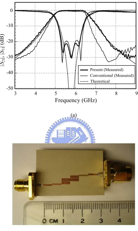
r o T = 1.31 T = 0.91 Stage 2 (Z = 90Ω)o o (Z = 50Ω)Stage 1 1 T = 0.9 T = 1.31 W/d G/d Stage 2 (Z = 50Ω)o T = 0.91 T = 1.01 1 T = 1.1 T = 1.31 T = 1.11 1 T = 1.2 T = 1.31 dConventional (Measured) 11 21 Present (Measured) Theoretical |S |, | S | (dB) 0 -10 -20 -30 -40 9 8 7 6 5 4 -50 Frequency (GHz) 3 (a) (b)
Fig. 3.6 (a) Theoretical and measured responses of filter α. (b) Photograph of the fabricated circuit. fo =
5.8GHz, N = 3 and ∆ = 30%. Circuit dimensions: W1 = 0.24 mm, G1 = 0.15 mm, W2 = 1.45 mm, G2 = 0.13
mm. The line width of the quarter-wave transformer is 0.8mm. Substrate: εr = 10.2, thickness = 1.27
Fig. 3.6(a) shows the theoretical and measured results of filter α. Quarter-wave transformers are used to match Zo = 90 Ω to 50 Ω at the input and output ports. In Fig.
3.6(a), the curve denoted by “theoretical” is obtained by (3.11), and those by “present” and “conventional” are measured responses of filters synthesized by the present method and the conventional method [7], respectively. The “present” response matches with the “theoretical” maximally flat response very well. The excess poles of |S11|
could result from the unequal even- and odd-mode phase velocities of the microstrip coupled stages. Detailed data show that the measured “present” filter has ∆ = 30.2%, very close to the design. The filter based on the conventional method [6-7] has ∆ = 26%,
mainly due to the use of frequency independent J-inverters for the coupled-line stages. This is consistent with the results reported in [13]. Fig. 3.6(b) is photograph of filter α.
3-2-2 Filter χ:
For a fifth-order filter, the QT condition is obtained as
2 3 2 2 2 1 5 2 1 2 1 2 3 2 2 1 3 cos sin ] ) [( ) )( ( 2 T T T θ θ T S S S S S S S + + + − = (3.22)
Using (3.22) and the maximally conditions (3.13a) ~ (3.13c), the maximally flat responses are well specified. From (3.18), θ = 1.2566 radian. There are two degrees of freedom for choosing the solutions. Fig. 3.7 plots the filtered solutions of S2, T2, S3 and
T3 for T1 ranging from 1.4 to 1.75. When Zo = 50 Ω, Zoe and Zoo for the first, second and
third stages are plotted together with the design graph in Fig. 3.8. It is found the gap size G/d for stage 1 is always less than 0.1 even the degrees of freedom in choosing the
solution are fully utilized. However, we choose a solution for the 5-order filter for validating the circuit synthesis. The characteristic impedances for each coupled stages are listed in Table 3.2 and detailed dimensions are in the figure caption of Fig. 3.9. Since some gap sizes, G1 = 0.001 mm and G2 = 0.005 mm, are far beyond the best
resolution of our fabrication facilities, only simulation responses are provided. Fig. 3.9 shows the theoretical and simulated results of this filter. If the conventional method is used, upon the requirement of ∆ = 40%, the bandwidth decrement could close to 10% [13]. While in our proposed method, the bandwidth is 40.5% which very close to the specification.
2
T
1 2 3 3 3 T 3 S T 3 2.5 2.0 1.5 1.0 0.5 1.75 1.7 1.65 1.6 1.55 1.5 1.45 2 2 SS
, T
, S
, T
0 1.4=1.4 1 T T1=1.75 T1=1.4 =1.75 1 T Stage 3 T1=1.75 T=1.41 W = 10.2 d r
ε
ε
r W G W/d G/dZ
20 40 60 80 100 120 140 160 20 40 60 80 100 0Z
0.1 0.2 0.3 0.6 1.0 2.0 0.4 0.1 0.2 0.3 1.0 2.0 1.5 0.7 0.5 oo oe(Ω)
0.15(Ω)
1 Stage 1 Stage 2Fig. 3.8 Root loci for Zoe and Zoo of the first, second and third stages of the fifth-order filter with ∆ = 40%
3 Frequency (GHz) -50 4 5 6 7 8 -40 -30 -20 -10 0 |S |, | S | (dB) 9 Theoretical 21 11 Synthesized(Sim.)
Fig. 3.9 Simulated and theoretical responses of the synthesized filter χ. fo = 5.8GHz, N = 5, ∆ = 40%.
Circuit dimensions: W1 = 0.767 mm, G1 = 0.001 mm, W2 = 1.94 mm, G2 = 0.005 mm, W3 = 2.1 mm, G3 =
3-2-3 Filter β:
For a sixth-order filter, the QT condition is
4 2 3 2 2 2 1 6 2 1 2 2 4 3 2 3 2 2 cos sin ] ) 2 [( ) ( ) )( 2 ( T T T T θ θ T S S S S S S + + + − = + (3.23)
There are three degrees of freedom for choosing the solutions. We take T1, S2 and T2 as
sweep variables in solving the simultaneous equations. If solutions with tough structural parameters are removed, the rest S2 ranges from 0.49 to 1.54 and T2 from
0.28 to 0.61, for 1.08 ≤ T1 ≤ 1.7. Three sets of solutions with (S2, T2) = (0.49, 0.28),
(0.96, 0.51) and (1.54, 0.61) are plotted in Fig. 3.10. Based on the design graph in Fig. 3.5 and Zo = 90Ω, we choose a solution for filter β for validating the circuit synthesis.
As shown in Fig. 3.11, the simulation results match very well with the theoretical prediction. The simulated response has a BW of 30.3%, i.e., only 0.3% away from the specification. The characteristic impedances for each coupled stage are listed in Table 3.2 and detailed dimensions are in the figure caption. Since some gap sizes, G1 =
0.06mm and G2 = 0.02mm, are far beyond the best resolution of our fabrication
3 S = 1.54, T = 0.61 S4 T 4 S4 T S4 4 T 4 S , T 4 0 0.5 1.0 1.5 2.0 1 T 1.7 1.6 1.5 1.4 1.3 1.2 1.1 1.0 3 S , T T3 S3 T3 3 S S = 0.49, T = 0.28 S = 0.96, T = 0.51 T3 3 S 4 1.0 0 0.5 1.5 2.0 2 2 2 2 2 2
Fig. 3.10 Root loci of S3, T3, S4 and T4 for a sixth-order filter with ∆ = 30% for (S2, T2) = (0.49, 0.28),
(0.96, 0.51) and (1.54, 0.61). 11 21 Synthesized (Simulated) Theoretical |S |, |S | (d B) 0 -10 -20 -30 -40 9 8 7 6 5 4 -50 Frequency (GHz) 3
Fig. 3.11 Simulation and theoretical responses of filter β. fo = 5.8GHz, N = 6, ∆ = 30%. Circuit
dimensions: W1 = 0.24 mm, G1 = 0.06 mm, W2 = 1.27 mm, G2 = 0.02 mm, W3 = 0.92 mm, G3 = 0.47 mm, W = 0.55 mm, G = 0.78 mm.
3-3 Implementation Using Tapped Input/Output
In many cases, such as Fig. 3.11, line widths or gaps are too small to fabricate, even the degrees of freedom in choosing the solution are fully utilized. This situation becomes more severe when order or BW is increased. Fortunately, the tapped input/output [15-16] can be used to resolve this problem. Theoretically, the tapping structure can realize a very wide range of the coupling coefficients. Thus, criterion for choosing the solution becomes to release dimensions of middle stages and locate the difficulties to the end stages as much as possible.
Since the derivation of the IL function (3.15) is based on a cascade of coupled stages, we have to establish the equivalence between a tapped resonator and a coupled stage. For the tapped structure in Fig. 3.12, let l be the distance between the tap point and one end of the resonator and Z1 be its characteristic impedance. It can be shown
that its impedance matrix elements can be written as
) cot cos (sin cos 1 11 jZ L Z =−
β
lβ
l+β
lβ
(3.24a) L Z j Z Z β β sin cos 1 21 12 = = − l (3.24b) L jZ Z22 = − 1cotβ
(3.24c)At the same time, the Z matrix elements of a coupled-line stage are (3.2a) and (3.2b). The equivalence of these two two-ports can be established by letting θ = βL = π/2, l = 0 and Z1 = (Zoe – Zoo)/2. The equivalence is, however, valid only for a finite frequency
and Zoo is 100Ω since S1 = 2 and Zo = 50Ω is expected. In Fig. 3.13, both cases have a
maximal |S21| deviation less than 0.08 dB and 0.34 dB within a BW of 50% and 100%,
respectively. These two tapped line structures will be employed to the following two experimental filters.
3-3-1 Filter δ:
This filter is designed to have N = 3 and ∆ = 50%. Based on (3.18), θ = 1.1781 radian, the S2 and T2 solutions for T1 varying from 1.1 to 1.6 are shown in Fig. 3.4. For
realization, the chosen roots and modal impedances are listed in Table 3.3 with Zo =
50Ω. A tapped resonator with Z1 = 39.68Ω is used to replace the end stages with Zoe1 =
89.68Ω and Zoo1 = 10.32Ω. Fig. 3.14(a) plots the theoretical, simulated and measured
responses. They have very good agreement within the passband. Detailed data show that the BWs of the simulated and measured results have only 0.5% and –0.5%, respectively, away from the theory. The measured midband insertion loss is about 0.35dB. Photograph of the fabricated filter is in Fig. 3.14(b). Note that the line gap 0.23mm is much easier to realize than the 0.13mm-gap of filter α. Thus, as compared with filter α, there are at least two advantages incorporating the tapped input/output into the design. One is that it greatly releases the tough circuit dimensions even though the BW is increased from 30% to 50%, and the other is that the impedance transformer can be saved since Zo = 50Ω.
l
L = /4
λ
Z
1port 1
port 2
Fig.3.12 A tapped line treated as a two-port network.
1 1 Tapped-line (l = 0, Z = 42.88Ω) ∆ = 50 % Coupled-stage (92.88Ω, 7.12Ω) Tapped-line (l = 0, Z = 39.68Ω) o 1.5 1.4 1.3 1.2 1.1 1.0 0.9 0.8 0.7 0.6 1.0 0.8 0.6 0.4 Coupled-stage (89.68Ω, 10.32Ω) 0.2 Insertion Loss (dB) 0
f / f
0.5Synthesized (Sim.) 11 21 Synthesized (Meas.) Theoretical
|S
|, |
S
| (dB)
0 -10 -20 -30 -40 9 8 7 6 5 4 -50Frequency (GHz)
3 (a) (b)Fig. 3.14 (a) Theoretical, simulated and measured responses of filter δ. fo = 5.8GHz, N = 3, ∆ = 50%. (b)