利用低成本高分子基板結合覆晶封裝技術之高頻及機械特性之探討
91
0
0
全文
(2) RF and Mechanical Evaluation of Low-Cost Polymer Substrate for High Frequency Flip-Chip Packaging. 研 究 生:胡志偉. Student:Oh Chee Way. 指導教授:張翼博士. Advisor:Dr. Edward Yi Chang. 國 立 交 通 大 學 材料科學與工程學系 碩 士 論 文. A Thesis Submitted to Department of Materials Science and Engineering College of Materials Science and Engineering National Chiao Tung University In Partial Fulfillment of the Requirements For the Degree of Master In Materials Science and Engineering August 2008 Hsinchu, Taiwan, Republic of China. 中 華 民 國 九 十 七 年 八 月.
(3) 題目:利用低成本高分子基板結合覆晶封裝技術之高頻 及機械特性之探討. 研究生:胡志偉. 指導教授:張翼 博士. 國立交通大學材料科學與工程學系. 摘要 本實驗主要探討低成本高分子基板 RO3210 應用於覆晶封裝結構之高頻特性的 研究。設計在 GaAs 晶片上的 CPW 傳輸線成功地以熱壓法與 RO3210 基板做 覆晶結合。通過適當的設計,高頻特性可被成功地提升。從 DC 到 67 GHz 的 S 參數量測中,反射損失(reflection loss, S11) 及 介入損失(insertion loss, S21) 皆有很好的表現(-20 dB 及 -0.8 dB)。此結果與我們的模擬結 果相互符合。此外,封裝在 RO3210 高分子基板上的主動式元件(m-HEMT)較 封裝前的 gain 僅少了 2 dB,呈現優秀的特性 。在這些結構中,被填入的 underfill 及 glob top 也同時被探討。在可靠度測試中:TCT (-55 °C to 125 °C, 600 cycles)及高溫高濕測試(8 5% RH/ 85 °C, 500 hours),填入了 glob top 材料後的覆晶結構在經過 200 個溫度循環測試後,由於高熱膨脹係數的 glob top 與高分子基板之間的熱應力而徹底壞掉,可觀察到破壞發生於金凸 塊與高分子基板的界面。但是,填入 underfill 的覆晶結構,可成功渡過高溫 循環測試,並有效地減低應力和提升可靠度。. i.
(4) RF and Mechanical Evaluation of Low-Cost Polymer Substrate for High Frequency Flip-Chip Packaging. Student: Oh Chee Way. Advisor: Dr. EdwardYi,Chang. Institute of Materials Science and Engineering National Chiao-Tung University. Abstract This work studies the selection and evaluation of new board materials RO3210 that enables flip chip packaging in microwave applications. A coplanar transmission line structure on GaAs chip were mounted on a RO3210 substrate using flip chip Au-to-Au thermal compression method. By using suitable layout optimization and compensation design, the S parameters performance of this structure was greatly improved. From DC to 67 GHz measurements, the resultant reflection loss S11 and insertion loss S21 exhibited excellent performance of -20 dB and -0.8 dB respectively. These results agreed well with the EM simulation data. Meanwhile, the flip chip bonding of in-house fabricated m-HEMT active devices on RO3210 also displayed excellent gain performance by small deviation -2 dB. Besides, the influence of encapsulant (underfill/ glob top) was also investigated. When epoxy resin encapsulant was injected into flip chip structure, the frequency band of the devices shifted to low side. To extend the use of this encapsulation method to high reliability and harsh environmental conditions, thermal cycling (-55 °C to 125 °C, 600 cycles) and ii.
(5) humidity test (85 % RH/ 85 °C, 500 hours) were carried out. The effect of board properties such as coefficient of thermal expansion (CTE) upon the reliability performance was investigated. Glob top encapsulation which found widespread acceptance in electronics assembly for low frequency packaging consumer products (wire bonding type packaging) showed poor performance as a result of large CTE difference between the board and encapsulant (completely failed at 200 cycles). Meanwhile, packages with underfill exhibited excellent bump interconnection reliability. It is well-understood that underfill materials can redistribute the stresses and hence enhance the reliability. Overall, both electrical and reliability tests demonstrated the feasibility of using RO3210 as microwave packaging substrate up to U-band applications.. iii.
(6) 誌. 謝 回顧這兩年的碩士研究生涯,秉持着人生師匠的一句話:“青年,要踏. 上世界的舞臺,”讓我更加有勇氣地堅信自己的信念,追逐來臺灣留學的夢想。. 來臺灣這一趟,非常感謝指導教授,張翼老師給與的機會。在實驗室的 大環境下去學習是一件很開心的事情。過程中,我經歷了如何調試自己的學習心 態及怎樣適應環境的挑戰。. 家人的支持及同學的鼓勵是協助我成長的原動力。在 Flip chip 組裏, 感謝共戰的夥伴:立翰學長、偉誠學長及吟竹學姐。從他們身上我學習到了他們 對研究的專業、認真、堅持及熱情。套上牛頓的一句話:“如果我看得比別人遠. 那是因為我站在巨人的肩膀上。”Flip chip 團隊裏,還有景德同學及思屏學 妹。大家都發揮了自己的專長、特色及角色。. 完成這份碩士論文,身邊出現很多諸天善神的守護:蔡先生熱情完成可 靠度測試、衍昇學長義無反顧協助濺鍍、廠商無條件提供免費的材料等等。我相 信一切事情的發生並非偶然。這過程當中,很懷念能與大家一起做研究的點點滴 滴:創价學會的夥伴,一起繼續努力;延儀,你是我的偶像;外籍學生組織,謝 謝您全力的協助我生活上的點滴;小噴學長,感謝你的幽默笑話;Dang, 很懷念 你的廚藝;同屆同學-小琪、大琦、小丸子、小禮、Vick、小鴨、敬哥、蕭蕭, 祝福你們前途無限光明。。。。. 今後,期許自己無論身在何處,都會發揮最高生命的價值,渡過一個無 怨無悔的人生。最後,感謝大家給與的關懷、鼓勵、提醒、協助、回憶。。。。. iv.
(7) Contents 中文摘要. i. Abstract. ii iv. 誌謝 Contents List of Tables List of Figures. v vii viii. 1. Introduction/ Background 1.1 Introduction 1.2 Aims of this work 1.3 Organization of this thesis. 1 1 1 2. 2. Theories and Paper Review 2.1 Microwave frequency 2.2 Microwave packaging 2.3 Chip level interconnect: flip chip 2.4 Motivation to lower cost substrate: organic substrate 2.5 Chip on board (COB) 2.6 COB encapsulant 2.7 Influence of flip chip structure in RF performance 2.8 Influence of material choice in RF performance 2.9 Total losses in microwave frequency. 3 3 3 5 6 8 9 10 12 13. 3. Experiment and Process Flow 3.1 Test die/ chip preparation 3.2 Evaluation of RO3210 substrate 3.3 Photolithography process: Au CPW and bump formation 3.4 Bare chip mounting 3.5 Encapsulation: Underfill injection/ Glop top application 3.6Electrical properties evaluation: DC/S parameter measurements 3.7 Environmental stressing: Thermal Cycling Test (TCT)/ Humidity test. 22 22 23 23 25 25 26 27. v.
(8) 4. Results (I): Packaged passive structure 4.1 Comparison of RF measurement data on RO3210/ Al2O3 4.2 Improved package design: RF performance of flip chip package with compensation design 4.2.1 Non encapsulated passive structure 4.2.2.1 Pad overlap, lob 4.2.2.2 Ground pad shrinkage, SL 4.2.2.3 Compensation at signal width, SW 4.2.2 Encapsulated passive structure. 39 39 41. 5. Results (II): Packaged active structure 5.1 S-Parameter Measurement of m-HEMT on RO3210 and Al2O3 5.2 S-Parameter Measurement of m-HEMT on RO3210 with underfill 5.3 S-Parameter Measurement of m-HEMT on RO3210 with glob top. 62 62 62. 6. Results (III): Reliability test 6.1 Thermal cycling test (TCT) 6.2 Humidity test. 68 68 70. 7.Conclusions References. 74 77. vi. 41 41 42 43 44. 63.
(9) List of Tables. 2.1 2.2 2.3 3.1 3.2 4.1 4.2. 4.3 4.4 4.5. 4.6 4.7 6.1 6.1 6.1 6.2. Microwave frequency band Material properties of conventional microwave packaging Comparisons of material properties of ceramic and polymer resin Composition and thickness of each layer in m-Hemt structure Material properties of underfill and glob top The parameters of CPW thru line on RO3210 and Al2O3 substrate S parameters performances at discrete microwave frequency applications (10 GHz, 20 GHz, 30 GHz and 40 GHz) on RO3210 and Al2O3 substrate Paper review on total loss caused by 2 levels of package transitions (Al2O3 based structure) Overall performance of three optimized designs lob = 50 μm, SL = 130 μm and SW = 30 μm Comparison of measured S11 and S21 of a mounted flip chip before and after the addition of underfill on a compensation at signal width structure, SW = 30 μm Chip gap modifications by pre-modified to 50 ohm Parameters modification in the structure (a) Evolution of bump contact resistance of the assemblies without encapsulation on RO3210 (b) Evolution of bump contact resistance of the assemblies with UF on RO3210 (c) Evolution of bump contact resistance of the assemblies with GT on RO3210 Evolution of bump contact resistance of the assemblies (without encapsulation/ with underfill/ with glob top on RO3210 in humidity test. vii. 17 17 17 29 29 47 47. 47 48 48. 48 49 71 71 71 71.
(10) List of Figures. 2.1 2.2 2.3 2.4 2.5 2.6 2.7 2.8. 2.9 3.1 3.2 3.3. 3.4 3.5 3.6 3.7 3.8 3.9 3.10 3.11 3.12 3.13. Hierarchy of electronic device packaging (a) Wire bonding technique (b) flip chip bonding Chip on board (COB)- wire bond type (a) Under-fill between chip and substrate (b) Cross section view (a) Glob top on a bare chip (b) Cross section view The FC interconnect and relevant parameters: bump height and pad overlap Material Parameters: Dk, tan δ, Dielectric thickness, CPW line width (a) Effective impedance of FC system and parameter modification (b) Pad overlap, lob (c) Signal Width Compensation, Cw and (d) Ground Pad Shrinkage, SL Chip loss, underfill loss and substrate loss in dielectric loss The layout (Drain, Gate and Source) of the m-HEMT The layout of CPW thru-line on GaAs chip (a) AFM image on RO3210 (Rms = 42.813 nm at 5 μm x 5 μm) (b) AFM image on Al2O3 as comparison (Rms = 8.965 nm at 5 μm x 5 μm) Process flow of Au CPW/ bump formation on RO3210 (a) SEM micrograph of bump formation on RO3210 (b) bump height Photo of RD automation M9 Bonding Machine SEM micrograph of GaAs flip chip on RO3210 substrate (a) SEM micrograph of underfill dispensing on flip chip (b) SEM micrograph of glob top dispensing on flip chip S-parameter measurement Agilent PNA network analyzer up to 67 GHz Resistance measurements on tested assemblies The Condition of TCT In house process flow of fabrication FC interconnects on RO3210 substrate Reliability test plan diagram viii. 18 18 18 18 18 20 20 21. 21 30 30 31. 32 33 34 34 35 36 36 36 37 38.
(11) 4.1 4.2 4.3. 4.4. 4.5 4.6 4.7 4.8 4.9 4.10 4.11 4.12 4.13 4.14 4.15 4.16 4.17 4.18 4.19. Top view of S measurement on 50 ohm CPW thru line on RO3210 and Al2O3 substrate Measured return loss S11 and insertion loss S21 results of the CPW thru-line on RO3210 and Al2O3 substrate Layout of flip chip configuration (without compensation) on packaged substrate: RO3210 and Al2O3 Measured return loss S11 and insertion loss S21 results of the flip GaAs chipped (without compensation) on RO3210 and Al2O3 substrate (a) SEM micrograph of CPW line on Al2O3 (b) CPW line on RO3210 Schematic diagram of various pad overlap, lob Simulated results on pad overlap at 50 μm, 70 μm and 90 μm Bump interconnect Equivalent circuit Measured return loss, S11 of FC bonded chip on pad overlap design substrate Measured insertion loss, S21 of FC bonded chip on pad overlap design substrate Schematic diagram of various ground pad shrinkage, SL Simulated results on various ground pad shrinkage, SL = 105 μm and 130 μm Measured return loss, S11 of FC bonded chip on ground pad shrinkage design substrate Measured insertion loss, S21 of FC bonded chip on ground pad shrinkage design substrate Schematic diagram of various compensation at signal width design, SW at 30 μm, 50 μm and 70 μm Simulated results on various compensation at signal width design, SW at 30 μm, 50 μm and 70 μm Measured return loss, S11 of FC bonded chip on a compensation at signal width design substrate Measured insertion loss, S21 of FC bonded chip on a compensation at signal width design substrate Measured performance of a mounted flip chip before and after the addition of glob top on a ground pad shrinkage structure, SL = 105 μm at substrate ix. 50 50 51. 51. 52 52 53 53 54 54 55 55 56 56 57 57 58 58 59.
(12) 4.20. 4.21. 4.22 4.23. 5.1 5.2 5.3 5.4 5.5 5.6 5.7 5.8 6.1 6.2 6.3. Measured performance of a mounted flip chip before and after the addition of glob top on a compensation at signal width design, SW at 20 μm at substrate Measured performance of a mounted flip chip before and after the addition of underfill on a compensation at signal width design, SW at 30 μm at substrate Application of glob top and underfill in the compensation structure Measured results on the compensation structure (chip modification and substrate layout optimization, compensation at signal width SW at 30 μm Top view of the developed packaged device structure The final photograph of the flip chip packaged m-HEMT device Comparison of gain in bare die and flip chip of m-HEMT on Al2O3 Comparison of gain in bare die and flip chip of m-HEMT on RO3210 Comparison of gain in bare chip and FC of m-HEMT (with underfill) on RO3210 Transconductance of the device with and without FC package (underfill) Comparison of gain in bare chip and FC of m-HEMT (with glob top) on RO3210 Transconductance of the device with and without FC package (glob top) Average resistances from bump contacts on RO3210 with temperature cycling Failure mechanism at CPW transmission line: delamination and crack Average resistances from bump contacts on RO3210 with humidity test at different hours (168 hours, 336 hours and 504 hours). x. 59. 60. 60 61. 64 64 65 65 66 66 67 67 72 72 73.
(13) Chapter 1 Introduction/ Background 1.1 Introduction. The rapid development of microwave technology had led to the revolution of wireless communication industry. It is becoming clear that the demand in microwave technology is moving to higher frequency, better performance and lower cost requirements. However, standard microwave packaging techniques based on ceramic housing had limited the deployment of very high frequency (> 30 GHz) systems due to its high material cost comparing to organic substrates. Based on Chip-on-Board (COB) technique, new packaging system based on organic substrate had been progressively investigated. The arising issue is mainly concerning on loss tangent of organic substrate which leads to the degradation in microwave performance and the thermal expansion coefficient (CTE) different between the chip and the organic substrate which leads to the mechanical failure. A well and basic studied needed to be carried out to investigate the potential and doubts of the implementation of organic materials.. 1.2 Aims of This Work. This work will focus on proposing a commercial polymer resin, RO3210 as a new 1.
(14) substrate for microwave packaging. A background study will be carrying out on RO3210 substrate to verify its potential usage, including: (i). Consideration of dielectric constant and loss tangent of RO3210. (ii) Significant of encapsulant properties (Dielectric constant and loss tangent) (iii) Simulation and improvement of flip chip structure on RO3210 (iv) Reliable packaging of the active device and passive devices on RO3210 Finally, this research will provide a reference or guideline of the robustness of COB technology in compatible with organic substrate for microwave packaging applications.. 1.3 Organization of this Thesis. This thesis is composed of seven chapters. Chapter 1 describes the background and aims of this study. In Chapter 2, an introduction to microwave frequency, microwave packaging, chip level interconnect: flip chip, motivation to lower cost substrate: organic substrate, COB, COB encapsulant, influence of flip chip structure in microwave performance, influence of material choices in microwave performance and total losses in microwave system. In Chapter 3, the experimental set up and process flow are presented. Chapter 4 and Chapter 5 present the experimental results and relevant discussion on packaged passive structure and packaged active device respectively. Meanwhile, reliability test data is presented in Chapter 6. The last chapter summarizes the research results and brings forward some issues for future studies.. 2.
(15) Chapter 2 Theories and Paper Review 2.1 Microwave Frequency. Less than a decade ago, the majority of activities at microwave frequencies was military related. However, the microwave industry has changed enormously following the boom in wireless communications. The frequencies of typical microwave applications include broadband radio links and distribution networks have moved up to 40 GHz and the automotive radar systems application is at 77 GHz.. According to Wikipedia, microwaves are electromagnetic waves with wavelengths ranging from 1 mm to 1 m, or frequencies between 300 MHz and 300 GHz. This microwave range includes ultra-high frequency (UHF) (0.3–3 GHz), super high frequency (SHF) (3–30 GHz), and extremely high frequency (EHF) (30–300 GHz) signals. Table 2.1 shows some microwave frequency bands, as defined by the Radio Society of Great Britain (RSGB).. 2.2 Microwave Packaging. Due to the rapid growth in the use of Internet and mobile communications, the semiconductor and packaging technologies have gained significant attentions. As a 3.
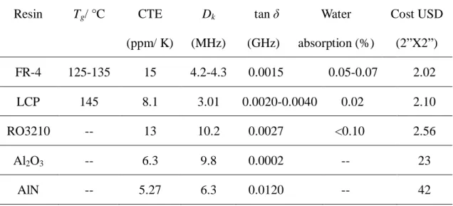
(16) whole, electronic packaging plays an important role in providing the interface between the IC and the rest of the system. In other words, packaging is the important signal passage and power dissipation interconnect for the IC systems. The packaging technology employed therefore, must withstand the thermal stresses resulting from the power ratings of the IC and the thermal expansion coefficient mismatch between the chip and the substrate. In addition, it must protect the IC from the environment which includes: shock, vibration, compression, moisture, temperature and provide an adequate space for the heat dissipation generated by the power IC systems.. Electronic packaging commonly includes several levels of interconnects. First level is the interconnection directly linked with the semiconductor chip. In many cases, the chip is mounted on an intermediate carrier substrate (ceramic substrate, lead frame etc), which is known as module. These modules are then assembled on board, where several modules are grouped to form a subsystem. The connection between modules and boards is named as the second interconnect level. Finally, these several subsystems will attach to a motherboard carrier to form the third level interconnect level (Figure 2.1).. According to International Microelectronic and Packaging Society (2005), packaging currently contributes to 35% to the total specific modules cost (other costs include: MMICs devices-45% & test/ tuning-20%), industries are interested in identifying possible cost reductions in electronic packaging while maintaining or improving functionality and reliability of the packaging system and ensuring volume production demands can be met in the manufacturing/market side.. 4.
(17) 2.3 Chip Level Interconnect: Flip Chip. At the chip level interconnect: tape automated bonding (TAB), wire bonding (WB) technique and flip chip (FC) bonding are among the favorites (Figures 2.2a & 2.2b). The FC technique is a MMIC chip mounted upside down on a carrier substrate (intermediate carrier/ multichip board) by using metallic bumps (solder or Au) as interconnects. This technique is well proven for lower frequencies. In fact, IBM introduced it in 1964 with its 360-mainframe generation known as C4, which stands for Controlled Collapse Chip Connection.. In the microwave field, however, FC is still rarely used. This is because the conventional technique cannot be transferred to microwave frequencies simply. Bump diameter and pitch have to be shrunk, and the bump metal-composition has to be modified in order to become compatible with millimeter wave and broadband chips [1].. On the other hand, although WB is a mature technology, it still offers some drawbacks such as: high parasitic effects, design limitation, low I/O density and large packaging size. FC bonding consequently is an option as it compensates these disadvantages [1]-[3] by offering: (i). Low performance losses in the RF device caused by the minimum interconnect length and inductance between bare-chip and the substrate can be achieved.. (ii). The mounting area of the package outline can be minimized and a smaller overall footprint can be realized. 5.
(18) (iii). High manufacturing through put can be expected thanks to the elimination of tuning and automation of the assembly process.. (iv). Its relevant parameters can be well controlled (bump dimensions). 2.4 Motivation to Lower Cost Substrate: Organic Substrate. Traditionally, conventional microwave packaging offers robustness FC based structure at chip level (CTE match for GaAs & Al2O3) and board level (matured PCB board Ball Grid Array, BGA technology) [4]. Material properties are listed in the Table 2. 2.. Ceramic based packages were introduced in [5] and [6] with high RF performances but required relatively high manufacturing costs. As the microwave applications are gradually transferring to consumer market, the packaging must meet the demands for high reliability, miniaturization, lower cost, low electrical loss and light weight [5].. Since 1930‘s, organic based substrate has become the back bone for component interconnections in products in 2nd level packaging. PCB is generally comprised of several layers of laminates. Laminate manufacturing is a process consisting of encapsulating a ply/ several ply of glass fabric within a polymeric resin [7]. Some of the most resins used in laminates today are Flame Retartdant-4 (FR-4) epoxy-hydrocarbon based, Liquid Crystal Polymer (LCP) based and Rogers (RO) series poly (tetra-fluoro-ethene) PTFE-based [Table 2.3]. 6.
(19) FR-4 epoxy is the most common commercial resin and its continuous high volume use over the past few decades has made its process compatible to PCB manufactures. FR-4 glass transition temperature (Tg) is 125-135 °C, dielectric constant (Dk) of 4.2-4.3 and loss tangent (tan δ) of 0.0015 [7][24].. LCP is another common resin in use today. LCP is the material which combines the properties of polymers with those of liquid crystals. LCPs are useful for electrical and mechanical parts, food containers, and any other applications requiring chemical inertness and high strength. This material displays Tg of 145 °C, Dk of 3.01 and tan δ of 0.0020-0.0040.. Meanwhile, RO series PTFE based materials were used for package construction in [8]-[9] recently. Differ from FR-4 and LCP, RO series substrate is a thermoplastic type polymer with high melting temperature (≈ 327 °C). This characteristic is preferable especially in high temperature fabrication of bump bonding in flip chip process (300 °C). The substrate in use in this research is RO3210 PTFE substrate. It offers high Dk of 10.2 and tan δ of 0.0027. In the design rule of Coplanar Waveguide (CPW) transmission line, a higher Dk property of substrate eases the CPW line parameter fabrication (Wider CPW gap width can be applied and controlled).. Although these organic substrates can reduce the material cost but it has large fluctuation in CTE , which induces fabrication inaccuracy and mechanical stress issue. This problem gives poor production yields as well as performance deterioration for the package. However, direct application of packaging to an organic substrate is still non-comprehensive. Tg has become another issue. The dramatically change in Tg will cause the resin changes from its glassy state to weak molecular-bonds state. This 7.
(20) will result in a change in the physical properties such as dimensional stability and flexural toughness.. 2.5 Chip on Board (COB). Mounting flip chip onto a low cost substrate not only enhance the electrical performances of the package but also reduce the production cost. This intention leads to the packaging technique called Chip on Board (COB). Historically, COB is referred to the process of wire-bonding a silicon die directly on a substrate material (no extra package used), after which the entire assembly is covered with an glob top resin material and cured to form a protective seal [Figure 2.3]. COB, in this particular case, is significant because it does not require to put the die into a package and the subsequent assembly of the package onto the PCB. As a result, it presents itself as a ‗package-less‘ IC packaging option.. The advantages of COB can be summarized as: (i). A reduction in manufacturing process, - die assembled directly to second level. interconnect, the PCB (save up material and fabrication cost) (ii). COB can be incorporated into Surface Mount Technology (SMT) lines.. (iii). Assembly miniaturization with reduction in size and weight. (iv). Improvement of electrical performance- package parasitic eliminated with. only one transition interconnect. Some efforts have been made to assemble active device and passive devices 8.
(21) onto PCB board by using Flip Chip on Board (FCOB) technique [8]-[12], but so far these attempts are not very successful. At present, introducing FCOB technology for microwave application is a technological challenge because it needs to overcome the CTE mismatch of chip (GaAs = 5.7 ppm/ K) and substrate (RO3210 = 13 ppm/ K) as compared to conventional packaging using alumina as substrates (Al2O3 = 6.3 ppm/ K).. 2.6 COB Encapsulant. Encapsulation is necessary with COB assemblies to provide both mechanical and environmental protection. The encapsulation, commonly divides into two categories called ‗Under-fill‘ & ‗Glob top‘.. Underfill is dispensed within the chip and substrate [Figure 2.4], which it redistributes the stress resulted from the difference of CTEs of the chip and substrate, and further increases the joint fatigue life. Second, it protects the interconnection from environmental damages such as vibration, moisture or shock. Third, underfill provides heat conducting paths between chip and substrate and helps with the heat dissipation.. Unfortunately, the use of underfill results in degraded performance due to dielectric losses, dispersion in wider bandwidth systems and de-tuning of circuits typically design of air [13]. Another important issue is the Dk of the underfill material, which should be as low as possible to avoid deterioration of RF performance at millimeter wave frequencies [14]. 9.
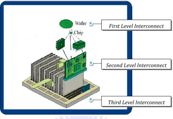
(22) Meanwhile, glop top is a technique derived from low frequency applications, which consists of dispensing an organic material as an encapsulant on a bare die [Figure 2.5]. The major function of the glob-top is to prevent delicate chip and the fine interconnection wire from chemical, electrical and mechanical damages. The chip surface and wire must not be directly subjected to corrosives such as moisture, dust and ionic contamination. As glob-top is the only component that provides this protection for the chip in COB, its reliability is critical. Desirable gob-top characteristics include low viscosity, adequate mechanical strength, good moisture resistance, good adhesion and fast cure without voids.. Among the encapsulant materials, epoxy based resin gives a promising characteristic as it shows excellent chemical resistance, excellent mechanical properties, excellent wetting for application and acceptable moisture barrier.. 2.7 Influence of FC Structure in RF performance. Electrical currents that oscillate at RF have special properties not shared by direct current signals. One such property is the ease with which it can ionize air to create a conductive path through air. Another special property is an electromagnetic force that drives the RF current to the surface of conductors, known as the skin effect. Third property is the ability to appear to flow through paths that contain insulating material, like the dielectric insulator of a capacitor. The degree of effect of these properties depends on the frequency of the signals.. 10.
(23) At microwave frequency, interconnects on the PCB and on the IC chip must be in the form of transmission lines to reduce signal reflection and maintain signal integrity [10]. Previous investigation [15] showed 50 Ω coplanar environment is necessary for optimized microwave performance.. Since FC interconnect influences RF behavior in a way of detuning effect and reflections/ insertion loss at the interconnect, circuits at FC requires much tighter control of parameters pertaining to signal losses. Ideally, the interconnect should be transparent to the electrical signals. In reality, however, each interconnect causes reflections. According to [1], bump‘s cross section does not play an important role for the electrical characteristics. Bump‘s height, h also causes negligible deviations in reflection losses. The parameter which determines reflection to first order is the pad size, Lp. Pad size refers to the pads on the motherboard and on the chip or the overlap of two metallization when referring to Figure 2.6 cause dielectric loading of the transition, which can be identified as the main source of the reflections.. Referring to [1], the FC interconnect can be described by an effective capacitance. This reactance results from the superposition of a capacitive and an inductive effect. The capacitive part is caused by dielectric loading at the transition due to the presence of both chip and motherboard dielectrics. The inductive contribution stems from the changes in current density distribution and direction when going from the motherboard line via the bump to the chip line.. In common structures, the capacitive effect is larger than the inductive. Hence, low reflections at the interconnect and low insertion loss are necessary for good high frequency characteristics but are not at all sufficient. It is because not only 11.
(24) the bump transition that determines millimeter wave characteristics but also the transmission line environments on chip and motherboard that plays an important role.. 2.8 Influence of material choices in RF performance. Besides design approach, materials selection can have a major influence on product cost, performance and time to market, too. There are some of the critical parameters which must be considered when selecting microwave laminate materials, including Dk, tan δ,dielectric thickness & trace width [16][17] [Figure 2.7].. Dk is a measure of the effect an insulating material has on the capacitance of a conductor embedded in the material or surrounded by it. It is also a measure of the degree to which an electromagnetic wave is slowed down as it travels through the insulating material. The higher the Dk, the slower a signal travels on a trace, the lower the impedance of a given trace geometry and the larger the stray capacitance along a transmission line. Given a choice, lower Dk is nearly always better [17].. tan δ is the second significant parameter needed to be paid attention. tan δ is a measure of how much the signal pulse (electromagnetic wave) propagating down the PCB transmission line will be lost in the dielectric region (PCB laminates).In other words, loss tangent is a function of the material‘s resin type and molecular structure (molecular orientation). Lower tan δ equates to more of the output signal getting to its destination.. α = 2.3 f ⋅ tan δ .Type equation here. Equation(1) 12.
(25) With,. α – Attenuation in dB / Inch. f – Frequency in GHz. tan δ – Loss Tangent of Material.. εeff – Effective Relative Er of Material. From the equation (1), the amount of signal losses in a circuit is not only a function of tan δ but is also a function of frequency and Dk of the materials.. Dielectric thickness (laminates thickness, H) and trace width (CPW line width) also play a key role in the transmission line impedance. A 20% change in dielectric thickness can cause as much as 12% change in impedance (Zo) [17]. As dielectric thickness increases, Zo increases. Meanwhile, A 20% change in trace width: signal width (WS), Ground width (WG) and Signal-to-Ground gap (WSG) can cause as much as 10% change in impedance. Hence, these traces width need to be well controlled during fabrication.. 2.9 Total Losses in Microwave Frequency. After understanding the effects of materials properties and the behavior in FC environment, this section will focus on total losses in the transmission of microwave frequency through CPW line in FC structure. Generally, a total loss in microwave signal follows Equation (2): Insertion/ Total loss, S21 = Reflection/ Return loss, S11 + Real loss. Equation (2). The two losses of greatest concern are losses caused by signal reflection, due to impedance mismatch and the loss of signal energy into the dielectric of the material. 13.
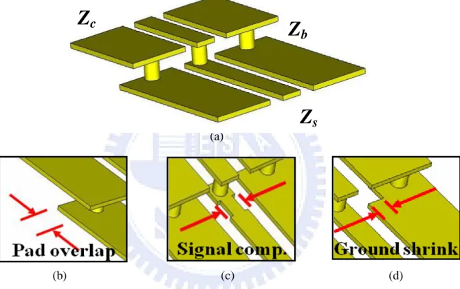
(26) Reflection loss is a result from impedance mismatching of the CPW line in FC environment, including: impedance at substrate (Zs), impedance at chip (Zc) and impedance at the bump transition (Zb). This loss can be improved by parameter modification at substrate side. Wolfgang et al. reported, by introducing parameter modification such as compensation at signal width (Cw) , pad overlap (lob) and ground pad shrinkage (SL), S11 can be significantly been improved [15][Figure 2.8].. On the other hand, when the under-fill is applied between the chip and substrate, the total impedance of the system changes effectively. It is because MMICs are usually designed for air with a permittivity of єr = 1 as the medium above the circuit. If the permittivity of the surrounding medium is increased due to encapsulation material, reflection effect becomes more pronounced since the dielectric material is in direct contact with the chip surface. One can tackle this problem by including the detuning in chip design a priori or by having a relatively thick dielectric layer (ex epoxy encapsulant) on top of the chip so that the influence of the under-fill is more or less negligible.. Meanwhile, the second pronounced loss which contributes to total loss is called real loss. This loss can be defined in Equation (3). Real loss = Metal loss + Dielectric loss + Radiation loss. Equation (3). Radiation loss is the attenuation that has very small effect, which usually can be neglected. In this case, metal loss and dielectric loss become dominant in microwave transmission line real loss.. Metal loss is the attenuation due to resistivity loss and skin effect. Voltage drop along the PCB trace, due to resistance in the trace is unavoidable. All metals 14.
(27) carry its own bulk resistivity (Cu = 1.673 μΩ-cm, Au = 2.44 μΩ-cm & Sn = 11.55 μΩ-cm). Higher bulk resistivity results in higher resistivity loss. However, from the DC through frequencies up to a few MHz, the current moves through the entire cross sectional area of the trace. At these frequencies resistance is extremely small, hence resistive losses are extremely small.. As frequencies increases (up to GHz), the energy moving in the trace is forced to the outer perimeter by the large magnetic fields present in higher frequency signals. This is known as skin effect because the majority of the energy is forced to the outer skin of the trace. From the equation R = ρ.L/A (R = resistance, ρ = Bulk resistivity, L = trace length, A = Cross sectional area of the trace), the reduced in cross sectional area of the trace will cause the resistance of conductor to be increased. This case is not favored in microwave frequency.. Dielectric loss is defined as the resonance losses for the ionic and electronic oscillation in the dielectric material. In short, this loss is due to movement or rotation of the atoms or molecules in an alternating electric field. This loss is contributed by chip loss, substrate loss and encapsulant loss [Equation 4] [Figure 2.9]. Dielectric loss = Chip Loss + Substrate Loss + Encapsulant Loss. Equation (4). Chip loss and substrate loss is induced from chip and substrate separately when microwave signal is propagating along the trace line. Choosing a low loss tangent in materials guarantees a low dielectric loss. With the higher loss tangent of the substrate in use in this research (RO3210 = 0.0027), the microwave performance is expected to be more severe compare to conventional microwave substrate (Al2O3 = 0.0002). As a result, the dielectric loss will be more pronounced in this organic 15.
(28) substrate.. Besides, the application of encapsulant in this flip chip structure will cause the permittivity of the surrounding medium to be increased. Few researches have been carried out to test the applicable of underfill [2][14] and glob top [21] in microwave packaging, and yet the mechanism, effect and reliability performance of encapsulant in microwave application is not well explained and studied through these papers.. 16.
(29) Table 2.1 Microwave frequency band Microwave Frequency Bands Designation. Frequency range. Designation. Frequency range. L band. 1 to 2 GHz. Q band. 30 to 50 GHz. S band. 2 to 4 GHz. U band. 40 to 60 GHz. C band. 4 to 8 GHz. V band. 50 to 70 GHz. X band. 8 to 12 GHz. E band. 60 to 90 GHz. Ku band. 12 to 18 GHz. W band. 75 to 110 GHz. K band. 18 to 26.5 GHz. F band. 90 to 140 GHz. Ka band. 26.5 to 40GHz. D band. 110 to 170 GHz. Resource: http://en.wikipedia.org/wiki/Microwave Table 2. 2 Material properties of conventional microwave packaging Chip :. 2nd level. 3rd level. GaAs. carrier: Al2O3. carrier: FR4. Dielectric constant, Dk. 12.9. 9.8. 4.2. Loss tangent (tan δ). 0.0020. 0.0002. 0.0015. CTE (ppm/ K). 5.7. 6.30. 15.00. Thermal Conductivity. 0.55. 18-35. 0.23. Cost USD (2‖X2‖). 88.9. 23.0. 2.02. Table 2.3 Comparisons of material properties of ceramic and polymer resin Resin. Tg/ °C. CTE. Dk. tan δ. Water. Cost USD. (ppm/ K). (MHz). (GHz). absorption (%). (2‖X2‖). 0.0015. 0.05-0.07. 2.02. 0.02. 2.10. <0.10. 2.56. FR-4. 125-135. 15. 4.2-4.3. LCP. 145. 8.1. 3.01. RO3210. --. 13. 10.2. 0.0027. Al2O3. --. 6.3. 9.8. 0.0002. --. 23. AlN. --. 5.27. 6.3. 0.0120. --. 42. 17. 0.0020-0.0040.
(30) First Level Interconnect. Second Level Interconnect. Third Level Interconnect. Figure 2.1 Hierarchy of electronic device packaging Resource: www.aciusa.org. (a). (b) Figure 2.2 (a) Wire Bonding technique. Resource: http://upload.wikipedia.org/wikipedia 18. 2.2(b) Flip Chip bonding.
(31) Figure 2.3 Chip on Board (COB) – Wire-bond type Resource: http://encyclopedia2.thefreedictionary.com/chip+on+board. Under-fill. Chip. Bump. substrate 2.4 (a). Under-fill. Chip. Bump. substrate 2.4 (b). Figure 2.4 (a) Under-fill between chip and substrate Resource: http://www.namics.co.jp/e/product/01/06.html 19. 2.4 (b) Cross section view.
(32) Glob Top. Chip. Wire Bond substrate (a). Glob Top. Chip Wire Bond. substrate (b) Figure 2.5(a) Glob top on a bare chip. 2.5(b) Cross section view. Resource: http://www.somar.co.jp/english/products/03_somatect.html. Figure 2.6 The FC interconnect and relevant parameters: Bump Height, h and Pad Overlap, Lp Resource: IEEE Microwave Magazine. 20.
(33) G. S. G CPW Dk. H. tan δ. substrate. Figure 2.7 Material parameters: Dk, tan δ, Dielectric thickness (H) &CPW line width. Zc. Zb. Zs (a). (b). (c). (d). Figure 2.8 (a) Effective impedance of FC system and parameter modification (b) Pad Overlap, lob (c) Signal Width Compensation, Cw and (d) Ground Pad Shrinkage, SL. Chip Loss Underfill Loss Substrate Loss. Figure 2.9 Chip loss, underfill loss and substrate loss in dielectric loss 21.
(34) Chapter 3 Experiment and Process Flow 3.1 Test Die/ Chip Preparation. Standard in-house fabricated active semiconductor devices, m-HEMT (High Electron Mobility Transistor) with well-known characteristics were chosen as the test dies. Monitoring the parameters of these devices at different stages of the assembly process (bare chips, after flip chip and after encapsulant) would give a clear indication of their electrical integrity. Any change or drift in the S-parameters values could be an indication of improper design of the packaging architecture.. Table 3.1 shows the composition and thickness of each layer in m-HEMT active device. The layout (including Drain, D; Source, S; Gate, G) of the device is shown in Figure 3.1.. Meanwhile, the fabrication of passive transmission line device was a GaAs chip containing CPW Au lines. Circuits for GaAs chip with dimensions WS = 75 μm, WG = 215 μm and WSG = 44 μm [Figure 3.2] were design using 50 Ω impedance transmission through line. These 50 Ω impedances characteristics of CPWs were simulated using CST Microwave Studio software.. 22.
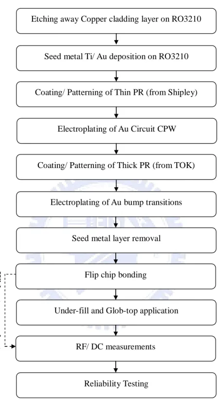
(35) 3.2 Evaluation of RO3210 Substrate. The substrate used in this research is RO3210 sheet from Rogers Corporation, Taiwan. The PCB RO3210 board came in copper electrodeposited (ED) cladding on the both sides of the sheet. The sheet thickness is 654 μm. This is the common PCB board that available in the market for DC industry. A mixture solution of water, sulfuric acid and hydrogen peroxide in a ratio 100: 5: 6 were used to etch away the copper cladding.. After the substrate preparation, an Atomic Force Microscopy (AFM) scanning was performed to evaluate the surface roughness of the RO3210. Figure 3.3 (a) shows the localized roughness, Rms of RO3210 (= 42.813 nm). The polished alumina substrate is also used for comparison (Rms = 8.965nm) [Figure 3.3(b)].. H. P. Chang et al. reported that the effects of surface roughness on RF MEMS switch performance [8]. In this study, the localized roughness of RO3210 is expected to be higher due to the limitation of AFM measurement equipment used. This surface roughness will not only degrade the RF performances, but will also affect the photolithography process in the near future.. 3.3 Photolithography process: Au CPW & Bump formation. In order to form the Au CPW transmission line, titanium (Ti) with thickness of 500 Å was used as the adhesion layer. On top of it, a thin layer of gold (Au) with thickness. 23.
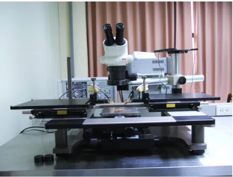
(36) of 2000 Å was deposited as the seed layer. Both layers were deposited by e-gun evaporator.. After that, the thin photo-resist from Shipley was spin coated at 1000 rpm for 10 seconds (1st spin) and 3000 rpm for 45 seconds (2nd spin) , followed by a baking at 90 °C for 4 minutes on a hot plate. The resist thickness was about 2-3 μm. The coated wafer was then exposed by the exposure tools: ABM aligner for 13 seconds. The substrate was post baked at 90 °C for 20 minutes on a hot plate. Next the substrate was subjected to a developer solution FHD-5. The resist film was rinsed with running DI water. The rinsed substrate was then immersed in a cyanide Au plating solution at 60 °C for 15 minutes with current flowed at 15 mA. After that, the photo-resist was stripped in an acetone solution and isopropyl alcohol (IPA) was used to eliminate the stripper solution.. For the Au bump formation process, the thick positive photo-resist, PMER PHA900PM was spin coated on the substrate at 500 rpm for 60 seconds (1st spin) and 2000 rpm for 2 seconds (2nd spin) , followed by baking at 120 °C for 10 minutes in an oven. This step is carried out twice to get a desired thickness of 30-40 μm. Again, the coated wafer was then exposed by the exposure tools: ABM aligner for 140 seconds.. Next the substrate was subjected to a developer solution PMER Developer P-7G. The resist film was rinsed with running DI water. The rinsed substrate was then immersed in a cyanide Au plating solution at 60 °C for 3 hours with current flowed at 1 mA. After that, the photo-resist was stripped in an acetone solution and isopropyl alcohol (IPA) was used to eliminate the stripper solution. After Au CPW transmission line and Au bump electroplating, Ti/ Au seed metal layers were removed in turn by 24.
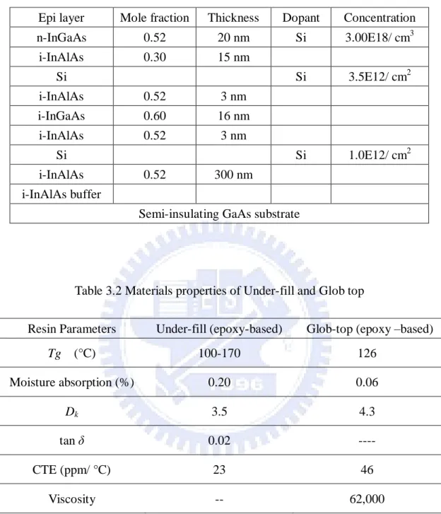
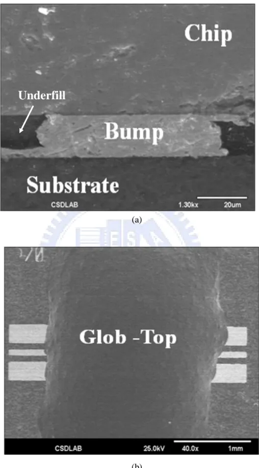
(37) potassium iodide /iodine, KI/ I2 solution (etch Au) and hydrofluoric acid (HCl), HF solution (etch Ti), respectively. The whole process flow is illustrated in Figure 3.4. Meanwhile, Figures 3.5 (a) & (b) show the SEM micrograph of the Au bump/ CPW line fabrication on RO3210 substrate.. 3.4 Bare chip mounting. The realization of the flip chip assemblies is based on the Au-Au thermo-compression bonding by RD automation M9 bonding machine in CSD lab [Figure 3.6]. The most important factor for bonding condition is the gap between the bare chip and the substrate. When bare chip-to-substrate distance is too close, RF performance of a bare chip maybe affect by Dk of the substrate.. The flip chip bonding conditions was keep constant throughout the experiments with heating temperature set at 250 °C (bare-chip)/ 250 °C (substrate). The bonding force was 150 gf/ sample. The bonding time was 150 s. Figure 3.7 shows the SEM micrograph of a successful flip chip on RO3210 substrate.. 3.5 Encapsulation: Under-fill injection/ Glob top application. The under-fill and glob top (molding compounds) chosen in this research is epoxybased resin. Table 3.2 shows the material properties of these two resins.. 25.
(38) First, 2 hours was provided for the under-fill to thaw once removed from the freezer. The test board was heated on a 100 °C hot plate to accommodate underfill wicking. This lowers the viscosity, allowing it to flow faster across the die. Finally test board was fully cured by heating in a 150 °C oven for 2 hours.. Meantime, the glob-top application on chip followed the same process flow as under-fill. Only at the final step, the test board with glob top was cured for 15 minutes. Figures 3.8 (a) & (b) show the SEM micrograph of underfill and glob-top dispensed on a flip chip.. 3.6 Electrical properties evaluation: DC and S parameter measurements. RF measurements were performed on a Agilent PNA connected to a Cascade probe station for a frequency range extending from DC to 67 GHz. [Figure 3.9] Measurements on assemblies (passive transmission line structures) were carried out before as well as after adding the under-fill/ glob-top encapsulant and environmental stress.. Meantime, the parameters of m-HEMT active devices ex., current gain, S21 and trans-conductance, Gm were measured too. DC measurements on each bump inter-connect was carried out to observe the changes in resistance before and after: encapsulant injection and environmental stress [Figure 3.10]. Figure 3.12 summarizes the in-house process flow of fabrication of flip chip Au bump interconnects on 26.
(39) RO3210 substrate.. 3.7 Environmental stressing: Thermal Cycling Test (TCT)/ Humidity test. To verify the reliability of flip chip construction in general, and the Au bump interconnections in particular, accelerated life tests were performed. The evaluation criterion was the increase of electrical resistance of the tested samples or the changes in S-parameters particularly. Either the time (in humidity test), or the number of cycles (in TCT test), to the first failure of a single bump interconnection was considered as a failure of the complete die [Figure 3.13].. The quality of Au bump interconnection was evaluated in the TCT. The integrity of the electrical contact was used as quality criterion. The TCT was maintained between -55 °C to +125 °C and the dwell time of 15 minutes (followed the JEDEC test conditions) [Figure 3.11].. The encapsulated packages were tested too. The main purpose of the underfill is to reduce mechanical stresses that will arise as a result of the different coefficients of the thermal expansion of the chip (GaAs) and substrate (RO3210). However the use of underfill cannot entirely eliminate the induced mechanical stress. It is well known that mechanical stresses change the electron and hole mobilities and are the basis of the piezo-resistive effect [18]. It is therefore reasonable to expect that the stresses induced in the die during assembly could influence the electrical performance of the 27.
(40) devices.. Besides, humidity tests (85 % RH /85 °C) were performed to check the influence of moisture absorption and permeability of the encapsulated materials (under-fill/ glob-top) on the performance of the flip chip architecture. Humidity plays an important role in the reliability of electronic circuits. It is omnipresent and can come from the ambient or from the materials used within the assembly process.. Chip on board devices are not hermetically sealed and thus are more likely to be affected by moisture diffusing from the ambient through the encapsulant. Water can also be absorbed and later released by the under-fill material and the PCB [18]. It is therefore very important to monitor the behavior of the devices in the presence of moisture.. 28.
(41) Table 3.1 Composition and Thickness of Each Layer in m-Hemt Structure Epi layer. Mole fraction. Thickness. Dopant. Concentration. n-InGaAs. 0.52. 20 nm. Si. 3.00E18/ cm3. i-InAlAs. 0.30. 15 nm Si. 3.5E12/ cm2. Si. 1.0E12/ cm2. Si i-InAlAs. 0.52. 3 nm. i-InGaAs. 0.60. 16 nm. i-InAlAs. 0.52. 3 nm. Si i-InAlAs. 0.52. 300 nm. i-InAlAs buffer Semi-insulating GaAs substrate. Table 3.2 Materials properties of Under-fill and Glob top Under-fill (epoxy-based). Glob-top (epoxy –based). 100-170. 126. Moisture absorption (%). 0.20. 0.06. Dk. 3.5. 4.3. tan δ. 0.02. ----. CTE (ppm/ °C). 23. 46. Viscosity. --. 62,000. Resin Parameters Tg. (°C). 29.
(42) Drain. Gate Source. Figure 3.1 The layout (Drain, Gate and Source) of the m-HEMT. GaAs Chip. WG. WS WSG. Figure 3.2 The layout of CPW thru-line on GaAs hip 30.
(43) 3.3 (a). 3.3 (b). Figure 3.3 (a) AFM image on RO3210 (Rms = 42.813 nm at 5 μm x 5 μm) AFM image on Al2O3 as comparison (Rms = 8.965 nm at 5 μm x 5 μm) 31. 3.3 (b).
(44) RO3210 substrate (I) Deposition of seed metal (Ti/ Au). RO3210 substrate (II) Patterning Thin photoresist. RO3210 substrate (III) Electroplating Au CPW and removal of thin photoresist. RO3210 substrate (IV) Patterning thick photoresist. 32.
(45) RO3210 substrate (V) Electroplating of Au bump and removal of thick photoresist and seed layer Figure 3.4 Process flow of Au CPW/ bump formation on RO3210. (a). 55.5 μm. (b) Figure 3.5 (a) SEM micrograph of Bump formation on RO3210 (b) Bump height 33.
(46) Figure 3.6. Photo of RD automation M9 Bonding Machine. Figure 3.7 SEM micrograph of GaAs flip chip on RO3210 substrate. 34.
(47) Underfill. (a). (b) Figure 3.8 (a) SEM micrograph of underfill dispensing on flip chip (b) SEM micrograph of glob top dispensing on flip chip. 35.
(48) Figure 3.9. S-parameter measurement Agilent PNA network analyzer up to 67GHz. Figure 3.10 Resistance measurements on tested assemblies. Figure 3.11 The condition of TCT 36.
(49) Etching away Copper cladding layer on RO3210. Seed metal Ti/ Au deposition on RO3210. Coating/ Patterning of Thin PR (from Shipley). Electroplating of Au Circuit CPW. Coating/ Patterning of Thick PR (from TOK). Electroplating of Au bump transitions. Seed metal layer removal. Without encapsulant. Flip chip bonding. Under-fill and Glob-top application. RF/ DC measurements. Reliability Testing. Figure 3.12 In-house process flow of fabrication flip chip interconnects on RO3210 substrate.. 37.
(50) Environmental Stresses (Reliability test). Thermal Cycling Test (TCT) (-55 °C—125 °C). . Humidity Test (85 °C/ 85 % RH). Visual/ OM inspection DC measurement. . 200 cycles. . Visual/ OM inspection DC measurement. 168 hours. Visual/ OM inspection DC measurement. . 400 cycles. Visual/ OM inspection DC measurement. 336 hours. . Visual/ OM inspection. . Visual/ OM inspection. . DC measurement. . DC measurement. 504 hours. 600 cycles. . Visual/ OM inspection DC measurement. . Visual/ OM inspection DC measurement. 9 modules (3 bare chips/ 3. 9 modules (3 bare chips/ 3. under-filled packages/ 3 glop-topped packages. under-filled packages/ 3 glop-topped packages. Figure 3.13 Reliability test-plan diagram. 38.
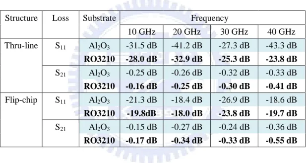
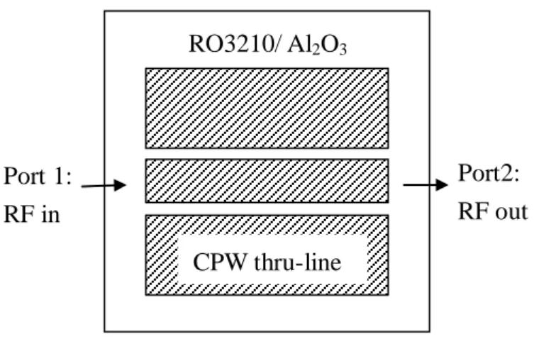
(51) Chapter 4 Result(I):Packaged Passive Structure. 4.1 Comparison of RF measurement data on RO3210/Al2O3. In order to investigate the RF performance on RO3210 substrates, a CPW thru line was designed and simulated with CST Microwave Studio simulation (characteristic impedance, Z0 = 50 Ω) before fabricating on RO3210 substrate. At the same time, Al2O3 substrate is also used for comparison with same CPW thru line design (characteristic impedance, Z0 = 50 Ω) applied [Figure 4.1].The parameters of CPW thru line on RO3210 and Al2O3 substrate are given in Table 4.1.. S parameters were measured by setting Port 1 as RF signal-in and Port 2 as RF signal-out at the end of each side along the CPW thru-line. Figure 4.2 shows the measured return loss S11 and insertion loss S21 results of the CPW thru-line on both substrates.. As can be seen from Fig. 4.2, a return loss of less than -20 dB is due to a good adaptation of the 50 Ω impedance. On the other hand, the insertion loss on both substrates suffers a same degree of degradation (approximately -0.5 dB before 40 GHz). Above 40 GHz, the insertion loss on RO3210 exhibits extra loss of -0.3 dB up to 67 GHz comparing to alumina. These results demonstrate feasibility of using RO3210 to substitute Al2O3 as a packaging substrate for microwave applications.. 39.
(52) After that, the thru-chip (GaAs), which is defined as having patterned CPW transmission line on the bare chip, was flip chipped and bonded on Al2O3 and RO3210 substrates [Figure 4.3]. Figure 4.4 shows the corresponding S parameters measurement results on these structures.. Comparing to the measured results of CPW thru-line (Fig 4.2), we can see that the flip chip structure exhibits reflection loss around -16 dB to -18 dB and insertion loss of -0.5 dB for both substrates. The bump transition at the flip chip structure causes extra performance degradation. Au bump interconnects have critical contribution to the performance of flip chip. The insertion loss here includes the propagation losses on the substrates, on the chip and through the Au bumps.. Table 4.2 summarizes the S-parameter data for discrete passive structures and CPW thru line on Al2O3 and RO3210 at microwave frequencies. The inferior performance of RO3210 can be explained by its inevitable material properties: higher loss tangent (0.0027) compared to Al2O3 (0.0002). Besides, the surface roughness of RO3210 will degrade the RF performance as RF signal is more difficult to transmit on a rough surface. The loss will be induced by the resistance of RF signal movement. Figure 4.5 shows the SEM micrograph of the surface roughness on RO3210 and Al2O3.. Generally, although RO3210 displays poorer S performances but the data is still in acceptable. These results demonstrates the possibility of using the RO3210 substrate as a packaging carrier at the 40 GHz range and indicate that even higher frequencies appear to be possible, at the expense of bandwidth, of course.. 40.
(53) From Table 4.3, Y. H. Suh et al., reported that alumina requires another level of package onto PCB board. The loss caused by 2 levels of package transitions is around 3.5 dB to 4.5 dB. Meanwhile, direct packaging onto organic substrate eliminates 1 level of transition and shows competitive performance to the 2 levels packages approach in RF applications. Reliability tests will be carried out later to evaluate the mechanical performances.. 4.2 Improved package design: RF performance of flip chip package with compensation. This section describes our effort in optimizing the transmission line performance by some compensation design (parameter compensation: lob, CW & SL) onto RO3210 substrate. Optimization was performed by means of 3D EM simulation (single transition). The goal is to achieve low reflection by downscaling the dimensions on RO3210. For measurement verification, a flip chip test structure was realized.. 4.2.1 Non-encapsulated passive structure 4.2.1.1 Pad overlap. The first parameter investigated here is the Pad Overlap, lob. This parameter is determined by the bump pad area (length and width) [Figure 4.6].Various lob at 50 μm, 70 μm and 90 μm were simulated and measured.. 41.
(54) Figure 4.7 presents simulation data of various lob (50 μm, 70 μm and 90 μm) used in the test structures. Changing the lob induces the parasitic capacitance. Figure 4.8 shows the bump interconnect equivalent circuit. Smaller pad overlap, 50 μm is preferable for high frequency flip chip application as the resultant parasitic capacitance, C is the minimum.. The measured data corresponds very well with the simulated data [Figure 4.9 & Figure 4.10]. The performance of reflection loss, S11 and insertion loss, S21 is enhanced by minimization of pad overlap at 50 μm by -18 dB and -0.45 dB up to 40 GHz respectively. After that, losses degrade significantly in both cases.. Since this design shows only small improvement in performance especially in higher frequency range (> 40 GHz), another structure design is proposed. The second design based on introducing the inductive effect to compensate the capacitive effect.. 4.2.1.2 Ground Pad shrinkage. The second parameter investigated here is the Ground Pad Shrinkage, SL. This parameter is determined by the ground pad area (length and width)[Figure 4.11]. Various Ground Pad Shrinkage at SL =105 μm and 130 μm was simulated and measured. Figure 4.12 presents the simulation data of various ground pad shrinkages used in the test structures. The results indicate that the reduction in ground pad width improves reflection loss, S11 significantly. It can be explained by shrinkage in transmission line on ground pad induces inductive effect to provide inductive counterpart compensating the parasitic capacitance.. 42.
(55) For measurement verification, the test structure as shown in Fig. 4.11 was fabricated. In Fig. 4.13 & Fig 4.14, the return loss, S11 and insertion loss, S21 are plotted. Good agreement between the data predicted by simulation and measurements were observed. The reflection loss is around -18 dB while the insertion loss is below -0.8 dB up to 50 GHz. The performance is slightly improved by this design especially up to 50 GHz applications. For SL =105 μm, the S21 performance before 45 GHz degraded, which could be explained by the non-uniform surface roughness.. 4.2.1.3 Compensation at signal width. The third parameter investigated here is the Compensation at signal width, SW. This parameter is determined by the length and width at signal width [Figure 4.15]. Various Compensation at Signal Width designs, SW = 30 μm, 50 μm and 70 μm were simulated and measured.. Simulated results display the influence of compensation at signal width, SW towards the S parameter performance. The shrinkage at signal width represents a high impedance effect to compensate the parasitic capacitance effects.. Higher. compensation at signal demonstrates higher impedance effect. Given a choice, higher compensation at signal is nearly always preferable.. In Figure 4.17 and Figure 4.18, both measured insertion loss and reflection loss are presented. The measurement data show good agreement with simulation results, which validates the model and proves accuracy of our finite-element time-domain code EM simulation.. 43.
(56) Quantitatively, the measured return loss for the signal compensated case improves beyond -18 dB around 50 GHz, given a broadband frequency application. Simultaneously, measured insertion loss has shown good performance of -0.7 dB up to 50 GHz. The performances of these three optimized designs are summarized in Table 4.4.. In brief, the design can be significantly improved after layout optimization and suitable compensation. The shrinkage at pad overlap introduces parasitic capacitance and performances (S11 and S21) up to 40 GHz are -20 dB and -0.5 dB respectively. But, as can be seen from the Table 4.4, the performance slightly degrades after that. In order to optimize the performance, introduction of high impedance line and inductance effect by compensation at signal width and ground pad shrinkage is carried out. The reflection loss, S11 is greatly improved (-0.6 dB). At higher frequency application, reduction in parasitic capacitance effect is visible but not so significant compared to the compensation by the inductance effect and the high impedance line. This is the best performance ever reported in the publications.. 4.2.2 Encapsulated passive structure. The investigation on the use of encapsulant (glob top/ under-fill) on a flip chip structure will be reported in this section. Figure 4.19 and Figure 4.20 shows the flip chip package with glob top and without glob top on a ground pad with structure shrinkage (SL = 105μm) and compensation at signal width structure (SW = 20 μm). The parameter of CPW transmission line on GaAs chip remains unchanged (WS = 75 μm, WG = 215 μm and WSG = 44 μm). 44.
(57) Comparing the measured results of the two flip chip assemblies with and without glob top on two different types of substrate layout, three kinds of effects due to glob top were observed: (i). The insertion losses degrade in a range -0.15 dB (Fig 4.19) and -0.32 dB (Fig 4.20) from DC to 67 GHz application. (ii) Obviously, the return losses degrade up to 20 GHz. After that, no significant difference in S-parameter was observed [Fig 4.19 and Fig 4.20]. (iii) Frequencies of minimum reflection shift 10 GHz to left side [Fig 4.19 and Fig 4.20]. The additional insertion loss is due to dielectric loss: glob top loss. The ―indirect interactions‖ between the CPW line and glob top acts to lower the line impedance. Thus, the performance will change when the glob top is added. On the other hand, at a first glance, it is surprising that reflection losses remain stable or slightly improved after glob top is applied (>20 GHz application). The reasonable explanation is that glob top material is treated as a ―natural compensation‖ to compensate the impedance mismatch at vertical bump transition region. This idea is first proposed in this study and further detailed studies need to be carried out. Besides, the reproducibility of the return loss is achieved by minimum reflection shift at 10 GHz. This is due to changes of the resonance frequency caused by the additional encapsulant applied.. Figure 4.22 shows the flip chip package with underfill and without underfill on a compensation at signal width structure (SW = 30 μm) respectively. The parameter of CPW transmission line on GaAs chip remains unchanged (WS = 75 μm, WG = 215 μm and WSG = 44 μm).. 45.
(58) Table 4.5 compares the measured results of the flip chip assemblies with and without underfill on substrate layout. The reflection loss S11 and insertion loss S21 performances in are listed in this table.. Obviously, both the S11 and S21 deteriorate from DC to 67 GHz application. This is due to extra underfill loss in the structure. The direct interactions between CPW lines with underfill encapsulant above them increase the dielectric loss. This is because the original design are designed for air dielectric (Dk = 1) above them. One method to overcome this problem is to design the chips with the effects of the dielectric underfill taken into account. This is done by pre-match to 50 Ω and with chip gap modification. The parameter of CPW line on GaAs chip has been changed (WS = 75 μm, WG = 215 μm and WSG = 84 μm) [Table 4.6].. Figure 4.22 illustrates the compensation structure (chip modification and substrate layout optimization) with glob top and underfill dispensing. Fig 4.23 shows the measured results of original design (chip modification and no substrate layout optimization) and compensation design (chip modification and substrate layout optimization, compensation at signal width SW = 30 μm) as a function of frequency [Table 4.7]. Clearly, the reflection loss is further improved due to chip impedance matching and ―natural compensation‖ of glob top. Both designs exhibits good reflection loss S11 which falls in a range of ≈ -15 dB. Especially, the compensation design has further improved the S11 performance after 50- 67 GHz (-20 dB). Simultaneously, the insertion loss S21 is further been reduced < -1.0 dB. The rule of thumb of chip impedance matching is by taking into the consideration of the effect of underfill into the design, and this approach has successfully enhanced the S parameters performance from DC to 67 GHz for broadband application. 46.
(59) Table 4.1 The parameters of CPW thru line on RO3210 and Al2O3 substrate Parameters (μm). RO3210 ( ZO = 50 Ω). Al2O3 (ZO = 50 Ω). WS. 70. 70. WG. 210. 210. WSG. 60. 33. Table 4.2 S-parameters performances at discrete microwave frequency applications (10 GHz, 20 GHz, 30 GHz and 40 GHz) on Al2O3 and RO3210. Structure Thru-line. Loss S11 S21. Flip-chip. S11 S21. Substrate. Frequency 10 GHz. 20 GHz. 30 GHz. 40 GHz. Al2O3. -31.5 dB. -41.2 dB. -27.3 dB. -43.3 dB. RO3210. -28.0 dB. -32.9 dB. -25.3 dB. -23.8 dB. Al2O3. -0.25 dB. -0.26 dB. -0.32 dB. -0.33 dB. RO3210. -0.16 dB. -0.25 dB. -0.30 dB. -0.41 dB. Al2O3. -21.3 dB. -18.4 dB. -26.9 dB. -18.6 dB. RO3210. -19.8dB. -18.0 dB. -23.8 dB. -19.7 dB. Al2O3. -0.15 dB. -0.27 dB. -0.24 dB. -0.36 dB. RO3210. -0.17 dB. -0.34 dB. -0.33 dB. -0.55 dB. Table 4.3 Paper review on total loss caused by 2 levels of package transitions (Al2O3 based structure). Publication. Package Structure. Loss caused by 2 package transition. Y.H. Suh et al [19] Chip: Substrate: PCB:. LNA MMIC Al2O3 HTCC RO4003. Gain deviation ≈ 4.5 dB. Chip: Substrate:. PA MMIC Al2O3 HTCC. Max gain deviation ≈ 3.5 dB. PCB:. RO4003 47.
(60) Table 4.4 Overall performance of three optimized designs lob = 50 μm, SL=130 μm and SW= 30 μm Optimized Design. Effect induced. Performance (dB) Loss. Original. -------. 20 GHz 30 GHz 40 GHz 50 GHz. S11. -19.4. -27.8. -18.4. -11.0. S21. -0.42. -0.46. -0.56. -1.19. Pad overlap. Parasitic. S11. -20.0. -38.9. -24.3. -13.3. (lob = 50 μm). capacitance. S21. -0.43. -0.43. -0.51. -0.87. Ground shrink. Inductance. S11. -19.5. -17.8. -23.1. -18.6. ( SL=130 μm). effect. S21. -0.34. -0.42. -0.46. -0.66. Compensation at. High. S11. -20.3. -25.5. -21.6. -22.0. S21. -0.30. -0.32. -0.44. -0.62. Sig. (SW= 30μm) Impedance line. Table 4.5 Comparison of measured S11 and S21 of a mounted flip chip before and after the addition of underfill on a compensation at signal width structure, SW= 30μm at substrate Structure. Performance (dB) Loss. 10GHz. 20 GHz 30 GHz 40 GHz 50 GHz. Without. S11. -20.4. -17.0. -18.2. -32.2. -17.7. Underfill. S21. -0.20. -0.37. -0.39. -0.41. -0.60. With. S11. -13.7. -11.9. -20.7. -16.9. -15.8. underfill. S21. -0.41. -0.67. -0.48. -0.62. -0.81. Table 4.6 Chip gap modifications by pre-modified to 50 ohm Parameter. Flip Chip Without underfill (air) With epoxy underfill. WS. 75 μm. 75 μm. WG. 215 μm. 215 μm. WSG. 44 μm. 84 μm. 48.
(61) Table 4.7 Parameters modification in the structure Substrate parameter. Chip parameter. Original design. Unchanged. Modified (50 ohm). Compensation design. Modified. Modified (50 ohm). 49.
(62) RO3210/ Al2O3. Port2: RF out. Port 1: RF in CPW thru-line. Figure 4.1 Top view of S measurement on 50ohm CPW thru-line on RO3210 & Al2O3. Figure 4.2 Measured return loss S11 and insertion loss S21 results of the CPW thru-line on alumina and RO3210. 50.
(63) Package substrate GaAs chip. Port2: RF out. Port 1: RF in. Figure 4.3 Layout of flip chip configuration (without compensation) on packaged substrate: Al2O3 and RO3210. Figure 4.4 Measured return loss S11 and insertion loss S21 results of the flip GaAs chipped (without compensation) on Al2O3 and RO3210. 51.
(64) (ai) Cross section view. (aii) Top view. (bi) Cross section view. (bii) Top view. Figure 4.5 (a) SEM micrograph of CPW line on Al2O3 (b) CPW line on RO3210. Chip side. Substrate side. lob Figure 4.6 Schematic diagram of various pad overlaps, lob 52.
(65) Figure 4.7 Simulated results on pad overlap at 50 μm, 70 μm and 90 μm. Chip CPW C. L Bump. Substrate. Figure 4.8 Bump Interconnect Equivalent Circuit. Reference: Copper flip chip bump interconnect technology for microwave subsystems including RF characterization [20] 53.
(66) Figure 4.9 Measured return loss, S11 of flip chip bonded chip on a pad overlap design substrate. Figure 4.10 Measured insertion loss, S21 of flip chip bonded chip on a pad overlap design substrate 54.
(67) Chip side. Substrate side. SL. Figure 4.11 Schematic diagram of various Ground Pad Shrinkages, SL. Figure 4.12 Simulated results on Various Ground Pad Shrinkages at SL = 105 μm and 130 μm. 55.
(68) Figure 4.13 Measured return loss, S11 of flip chip bonded chip on a Ground Pad Shrinkage design substrate. Figure 4.14 Measured insertion loss, S21 of flip chip bonded chip on a Ground Pad Shrinkage design substrate 56.
(69) Chip side. Substrate side. SW. Figure 4.15 Schematic diagram of various Compensations at Signal Width design, SW at 30 μm, 50 μm and 70 μm. Figure 4.16 Simulated results on various Compensations at Signal Width design, SW at 30 μm, 50 μm and 70 μm 57.
(70) Figure 4.17 Measured return loss, S11 of flip chip bonded chip on a Compensation at Signal Width design substrate. Figure 4.18 Measured insertion loss, S21 of flip chip bonded chip on a Compensation at Signal Width design substrate 58.
(71) Figure 4.19 Measured performance of a mounted flip chip before and after the addition of glob top on a ground pad shrinkage structure, SL = 105 μm at substrate. Figure 4.20 Measured performance of a mounted FC before and after the addition of glob top on a compensation at signal width structure ,SW = 20 μm at substrate 59.
(72) The second approach is to add in the underfill material into flip chip structu. Figure 4.21 Measured performance of a mounted flip chip before and after the addition of underfill on a compensation at signal width structure , SW = 30μm at substrate. underfill. chip. Glob top. substrate. Figure 4.22 Schematic diagram of application of glob top and underfill in the compensation structure. 60.
(73) Figure 4.23 Measured results on the compensation structure (chip modification and substrate layout optimization, compensation at signal width SW = 30 μm). 61.
(74) Chapter 5 Results (II): Packaged active structure In this section, the in-house fabricated active devices (m-HEMT) are packaged (with and without encapsulant) onto RO3210 and Al2O3 (as comparison). Comparable electrical gain was measured and will be presented in this Chapter. Figure 5.1 shows the schematic of the top view of the developed packaged device structure. Meantime, the final photograph of the flip chip packaged m-HEMT is shown in Figure 5.2.. 5.1 S-Parameter Measurement of m-HEMT on RO3210 and Al2O3. Figure 5.3 and Figure 5.4 show the results of packaged m-HEMT on Al2O3 and RO3210 substrate respectively. From both figures, the m-HEMTs after ―flipchipping‖ show small degradation compared to on-wafer (bare die) measurement as a result of extra reflection loss at bump transition interconnect. Although the deviation loss in gain is smaller in Al2O3 ( -1.5 dB) compared to RO3210 ( -2.0 dB), the performance is still in an acceptable range for commercial application.. 5.2 S-Parameter Measurement of m-HEMT on RO3210 with underfill. After ―underfilling‖, the performance degrades around -1 dB from DC to 40 GHz compared to the flip chip without underfilling [Figure 5.5]. This is understandable, as the dielectric loss become more obvious as a consequence from the loss of the 62.
(75) underfill material. The transconductance profiles of the m-HEMT after flip chip bonding shifted a little to a more positive gate bias [Figure 5.6].. 5.3 S-Parameter Measurement of m-HEMT on RO3210 with glob top. After ―glob-topping‖, the performance degrades around -2 dB compared to flip chip without glob topping in DC to 40 GHz application [Figure 5.7]. This result indicates that the dissipation factor of the glob top resin increases the transmission loss. The transconductance profiles of the m-HEMT after flip chip bonding shifted a little to a more positive gate bias [Figure 5.8].. Once again, it is confirmed that the underfilling and glob top resin used in this evaluation degrades the RF performance of flip chip packaged m-HEMTs. Underfill has been proven to have good performance (low losses) for high frequency application by Y.C.Hu [22]. And yet, so far very little attempt has been made to improve the glob top resin performance for high frequency application. Extra efforts on Dk and loss tangent of glob top are needed for the development for underfill for microwave applications. If underfilling is necessary, electrical characteristics of the resin must be considered in the design of m-HEMTs bare chip or lower Dk encapsulant resin is required.. 63.
(76) Electroplated Au bump. Electroplated Au line. GaAs m-HEMT. Figure 5.1 Top view of the developed packaged device structure. RO3210. Chip. Figure 5.2 The final photograph of the flip chip packaged m-HEMT device. 64.
(77) Figure 5.3. Figure 5.4. Comparison of gain in bare die and flip chip of m-HEMT on Al2O3. Comparison of gain in bare die and flip chip of m-HEMT on RO3210 65.
(78) Figure 5.5 Comparison of gain in bare die and FC of m-HEMT (with underfill) on RO3210. Figure 5.6 Transconductance of the device with and without FC package (underfill). 66.
(79) Figure 5.7 Comparison of gain in bare die and FC of m-HEMT (with glob top) on RO3210. Figure 5.8 Transconductance of the device with and without FC package (glob top). 67.
數據
+7
相關文件
二專 工業機械 二技 工業電子科技(高級技術員) 二專 汽車製造維修 二技 無塵室設備(高級技術員) 二專 紡織機械 二技 自動化科技電子(高級技術 二專 機電整合 二技
A “charge pump”: a device that by doing work on the charge carriers maintains a potential difference between a pair of terminals.. Æan emf device
Maintain an unvisited vertice set (intially, ) Maintain an array , where stores the current. known shortest path from the source
Therefore, a study of the material (EPI) re-issued MO model for an insufficient output of the LED chip manufacturing plant is proposed in this paper.. Three material
Atomic structure of hydrous ruthenium oxide coating on CNT substrate with 5 minutes of deposition period, (a) HRTEM image of specimen and (b) higher magnification of HRTEM
Zhong, "Design for Enhanced Solder Joint Reliability of Integrated Passives Device under Board Level Drop Test and Thermal Cycling Test," Electronics Packaging
(EV3)300MHz ARM9-based Sitara AM1808 system-o n-chip and CC2560 Bluetooth chipset, 64MB of RAM, 16MB of internal flash, and a 32GB micro SD
Lee, ”Effects of Build-Up Printed Circuit Board Thickness on the Solder Joint Reliability of a Wafer Level Chip Scale Package (WLCSP),” IEEE International Symposium
