國 立 交 通 大 學
電子工程學系 電子研究所
碩 士 論 文
含奈米粒子之先進奈米元件結構
應用於太陽能電池之研究
The Research of Advanced Nanodevice Structure
with Nanoparticles for Solar cell Applications
研 究 生: 詹政邦 (Cheng-Pang Chan)
指導教授: 吳重雨教授 (Prof. Chung-Yu Wu)
李耀坤教授 (Prof. Yaw-Kuen Li)
含奈米粒子之先進奈米元件結構
應用於太陽能電池之研究
The Research of Advanced Nanodevice Structure
with Nanoparticles for Solar cell Applications
研 究 生:詹政邦 Student:
Cheng-Pang
Chan
指導教授:吳重雨教授
Advisor:
Prof.
Chung-Yu
Wu
李耀坤教授 Prof.
Yaw-Kuen
Li
國立交通大學
電子工程學系
電子研究所
碩士論文
A Thesis
Submitted to Department of Electronics Engineering and Institute of Electronics
College of Electrical and Computer Engineering
National Chiao-Tung University
in Partial Fulfillment of the Requirements
for the Degree of
Master
in
Electronics Engineering
September 2008
Hsin-Chu, Taiwan, Republic of China
中華民國九十七年十月
含奈米粒子之先進奈米元件結構
應用於太陽能電池之研究
學生:詹政邦
指導教授:吳重雨
教授
李耀坤
教授
國立交通大學
電子工程學系電子研究所
摘 要
在本論文中,使用硒化鎘量子點和金奈米粒子,透過離子作用力建構多層太陽能電 池奈米元件結構於矽基板上。並且以不同粒徑之硒化鎘量子點依序排列組成此奈米結 構,用以實現寬頻吸收光譜太陽能電池。在掃描式電子顯微鏡的觀察下,證明其結構成 功地生長於矽基板上。最後,此奈米元件再經過0.16 mW/cm2日光燈照射後,於各種偏 壓下皆有固定的光電流增加。在本研究中,太陽能電池功率轉換效率達1.6 % (六層結構 奈米元件,電極寬度為30μm,長度為 0.5μm),最大光電流為 664.42 pA,光電流量體積 密度為7.385×10⁻¹⁹ A/nm3,以及單位體積產生功率為4.256×10-23 W/nm3。經過24 天,太 陽能電池效率衰減了31.8%。而經過 26 天之後,衰減現象趨於平緩飽和。 根據實驗結果我們發現奈米元件之電極距離縮短有助於太陽能電池功率轉換效率 之提升。再此同時,我們建構ㄧ個等效電路並成功地解釋奈米元件產生光電流的運作機 制,我們稱之為三維「奈米蕭特基二極體」和電組陣列模型,而且HSPICE 模擬結果與 量測結果一致。理論上透過模擬可得到最佳化的奈米元件結構,具有較高的太陽能電池 轉換效率。最後經過模擬計算此六層結構之奈米元件效率可達 36.87 % 當電極距離為 40 nm,而 51.17 % 當距離縮短至 30 nm。The Research of Advanced Nanodevice Structure
with Nanoparticles for Solar cell Applications
Student:
Cheng-Pang
Chan
Advisor:
Prof.
Chung-Pang
Wu
Prof. Yaw-Kuen Li
Department of Electronics Engineering and Institute of Electronics
National Chiao-Tung University
A
BSTRACT(English)
In this thesis, PDDA-capped CdSe/ZnS quantum dots and Au nanoparticles are used to construct the multi-layer solar cell nanodevice structure on a silicon substrate through ionic interaction. And an ordered assembly of PDDA-capped CdSe/ZnS QDs with different diameters was employed to realize the wideband solar cell. By SEM photographic, PDDA-capped CdSe/ZnS QDs and Au NPs were successfully deposited on the silicon substrate. Finally, the proposed nanodevices were illuminated by 0.16 mW / cm2 daylight lamp. As a result, there was a constant photocurrent increment to the current measured in the dark for each voltage bias after illumination by 0.16 mW / cm2 daylight lamp. In this work, the solar cell efficiency is 1.6% (6-layered PDDA-capped CdSe/ZnS nanodevice with 60 μm in width and 0.5 μm in length.) The maximum photocurrent is 664.42 pA. The highest PVD (photocurrent volume density) is 7.385×10⁻¹⁹ A/nm3, and power volume density is 4.256 ×10⁻²² W/nm3. After 26 days, 31.8% decrease in solar cell efficiency. And after 26 days, the decay tended to saturate.
Meanwhile, according to the experimental results, we knew that the shorter length of the nanodevice would benefit the performance of the solar cell efficiency. Furthermore, a three-dimensional“nano-schottky-diode"arrays equivalent circuit model was constructed and used to explain the photo-sensing mechanisms. Through HSPICE simulation, the higher
solar cell efficiency can be obtained based on the ideal inference. In conclusion, the optimized device dimension could be chosen, and we found that the solar cell efficiency was up to 36.87 % in 6-layered PDDA-capped CdSe/ZnS QDs and Au NPs with 30 μm in width and 40 nm in length. The solar cell can achieve high efficiency based on the model calculation.
A
CKNOWLEDGEMENTS
致謝
在碩士生涯中,首先要感謝我的兩位指導教授吳重雨校長和李耀坤教授,兩年多 來對我的耐心指導與諄諄教誨,使我於跨領域前瞻的研究過程中,得到源源不絕的靈 感與專業知識的奧援,帶領我順利完成碩士學業。其次要感謝許鉦宗教授、張國明教 授擔任我的口試委員,並提供許多寶貴的建議,使這篇論文的內容更加完整,真的很 感謝您們! 接下來要感謝李耀坤老師實驗室的靜萍學姊,給予我最大的幫忙與經驗分享,以 及多次提供NPs、QDs 和實驗支援的沈模沅學弟,讓我在研究的路途中走得更加順利 。感謝奈米所陳振嘉學長於實驗上的建議和協助;羅正忠老師實驗室的智仁學長、佳 樺、欣富、小陸,在製程技術上幫助我解決很多問題;百忙中抽空幫我拍 SEM 的材 料所學姊陳蓉萱;NDL 陳世哲先生協助我完成光罩設計與製作;刁維光老師實驗室的 呂學沛學長提供solar simulator,感謝你們總給予我不求回報的幫助,真的很謝謝你們 。當然也要感謝『奈米電子與晶片系統實驗室』的林俐如、王文傑、虞繼堯、蘇烜毅 、黃祖德、陳旻珓、陳勝豪、楊文嘉、蔡夙勇、陳緯明、金毛、顏承正等學長姊們, 在各方面給予許多幫助與指導,也感謝碩士班的同學們,謝謝神童傳授的秘技、維德 、順哥、阿部忠、晏維、宗裕、豪哥、松諭、巧伶學長姊在學業上給予我的指導。感 謝我們 group 的小帆、宅帥、建名、諶哥,感謝北鴨與世範陪我一起健身,感謝幫我 買衣服的小州哥,強大的歐威,人生經驗豐富的歐陽,偷偷來的科科和宗恩,FTP 很 大的紹岐,強力嘴炮+小熱褲的塔哥與暴力老大,還有禽獸和屌哥。此外,謝謝筱妊 、潮男昀、a-dair、天哥、林良、昕爺、kitty、佳琪、彥偉、小狗達、癡漢、明翰、 慧君、子薰等學弟妹們,也感謝永遠的室友主任和老爹,大家在苦悶的碩士生活中帶 給我許多歡笑。 最後,要獻上最深最深的感謝給我的父母親,詹明章先生與陳玉秀女士,我的妹 妹蕙慈和孟儒,提供最棒的環境,使我無後顧之憂地專注於學業上。還要感謝貼心的 彥琳,當我面臨龐大壓力時給予我的鼓勵與支持。感謝所有的親朋好友,謝謝你們的 關心,成為我最大的後盾。 詹政邦 誌於 風城交大 2008 秋C
ONTENTS
ABSTRACT (Chinese) ... i
ABSTRACT (English) ... ii
ACKNOWLEDGEMENTS ... iv
CONTENTS ... v
TABLE CAPTIONS ... vii
FIGURE CAPTIONS ... viii
CHAPTER 1 INTRODUCTION ... 1 1.1 Background ... 1 1.2 Reviews on Nanodevice ... 3 1.3 Motivations ... 5 1.4 Thesis Organization ... 5 CHAPTER 2 NANOPARTICLE SYNTHESIS AND NANODEVICE FABRICATION TECHNOLOGY ... 10
2.1 The Synthesis of Citrare-Capped Au Nanoparticles ... 10
2.2 The Synthesis of AET-CdSe and PDDA-CdSe Quantum Dots ... 11
2.3 The Physical Characteristic of Au Nanoparticles and CdSe/ZnS Quantum Dots ... 12
2.4 Nanodevice Fabrication Technology ... 15
2.5 Self-Assembly Process for Advanced Nanodevice Structure ... 16
2.6 Reaction Environment Investigation ... 17
CHAPTER 3 EXPERIMENTAL RESULTS AND DISCUSSIONS ... 36
3.1 The Environment Setup for Measurement ... 36
3.2 SEM Images And Optical Absorption / Emission Spectra ... 37
3.3 Nanodevice Performance Measurement ... 39
3.4 Nanoparticle Solar Cell Efficiency Estimation and Nanodevice Model Construction40 CHAPTER 4 APPLICATION OF LINEAR REGULATOR ON NANOPARTICLE SOLAR CELL ... 63
4.1. System Design Considerations ... 64
4.1.1. Architecture ... 64
4.1.2. AC Analysis ... 65
4.1.3 Transient Analysis ... 68
4.2 Circuit Blocks ... 70
4.3 Simulation Results ... 72
CHAPTER 5
CONCLUSIONS AND FUTURE WORKS ... 89
5.1 Conclusions ... 89
5.2 Future Works ... 91
REFERENCE ... 93
T
ABLE
C
APTIONS
Chapter
2
Table 2.1 The dimensions of all horizontal electrodes fabricated in NDL are list in this table. (unit:μm) ... 20
Chapter
3
Table 3.1 The experimental and measurement results of the proposed 6-layered PDDA-capped CdSe/ZnS nanodevices. (PVD: photocurrent volume density, Power VD: power volume density) ... 43
Table 3.2 Performance comparison table ... 43
Table 3.3 The simulation results with linear estimation of the proposed 6-layered PDDA-capped CdSe/ZnS nanodevices. ... 44
Chapter
4
Table 4.1 The specification of the error amplifier ... 75
Table 4.2 The specification of the feedback loop. ... 75
Table 4.3 Specification of the low dropout linear regulator system. ... 75
Table 4.4 The parameter of each device ... 76
F
IGURE
C
APTIONS
Chapter 1
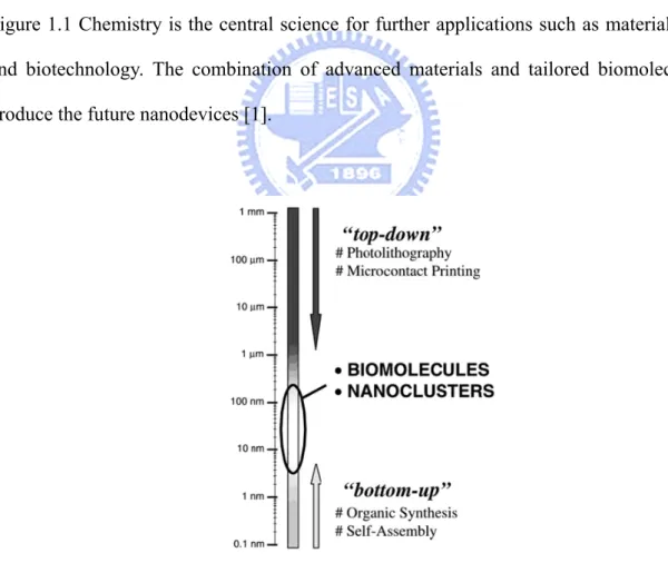
Figure 1.1 Chemistry is the central science for further applications such as materials science and biotechnology. The combination of advanced materials and tailored biomolecules will produce the future nanodevices [1]. ... 7 Figure 1.2 A gap currently exists in the engineering of small-scale devices. The
top-down processes will have their limit below 100 nm, and the bottom-up processes will also have a limit at 2~5 nm. The gap will be filled by nanoclusters and biomolecules [1]. ... 7 Figure 1.3 The efficiency evolution of best research cells by several of technology types.
This figure identifies those cells that have been measured under standard conditions and confirmed at one of the word’s accepted centers for standard solar-cell measurements [5]. ... 8 Figure 1.4 (a) Linking CdSe QDs to TiO2 particles with bifunctional surface modifier
(HS-R-COOH); (b) Light harvesting assembly composed of TiO2 film functionalized with CdSe QDs on Optically Transparent Electrode (OTE) [8]. (Not to scale) ... 8 Figure 1.5 Transmission electron micrographs of (A) CdSe and (B) CdTe nanocrystals
in ths investigation [9]. ... 9
Chapter 2
Figure 2.1 The flow diagram for preparing the citrate-capped Au NPs solution ... 20 Figure 2.2 (a) The close photographs of 100 μL of approximately 15 nm diameter Au
NPs solution + 100 μL DI water (left) and 100 μL of approximately 5 nm diameter AET-CdSe/ZnS NPs solution + 100 μL DI water (right). The Au NPs solution was in deep red while the AET-modified CdSe/ZnS NPs solution was in yellow. (b) The close photographs of the mixture of 100 μL Au NPs solution and 100 μL AET-modified CdSe/ZnS NPs solution just after mixing (right), the mixture after standing 6 hrs (middle) in room temperature, and the mixture after standing 5 days in room temperature (left). As we can see, the color of mixture just after mixing was like that of Au NPs solution. However, after 6 hrs, it became dark purplish red. After 5 days, there was obvious precipitate at the bottom and the supernatant became pale yellow. .... 21 Figure 2.3 (a) The TEM image of Citrate-capped approximately 15 nm diameter Au
NPs and the TEM image of AET-capped approximately 5 nm diameter CdSe/ZnS QDs. (b) The UV-visible spectrum of Au NPs solution. (c) The UV-visible and PL intensity spectrum of AET-CdSe/ZnS QDs solution. ... 22
Figure 2.4 (a) The band gap and surface structure diagram of CdSe/ZnS QD. (b) The PL intensity spectrum of different kind of surface capping method of CdSe QD . 23 Figure 2.5 The flow diagram for preparing the AET-capped CdSe/ZnS QDs solution. .... 24 Figure 2.6 Density of states in metal (A) and semiconductor (B). In each case, the
density of states is discrete at the band edges. The Fermi level is in the center of a band in a metal, and so kT will exceed the level spacing even at low temperature and small size. In semiconductor, the Fermi level lies between two bands, so that there is large level spacing even at large size. The HOMO-LUMO gap increases as the size of semiconductor nanocrystal decreases (bellow 10 nm). [11]. ... 25 Figure 2.7 The cross-section view of the electrode structure and the PR is photoresistor
for lift-off process. ... 26 Figure 2.8 (a) The cross section figure of the electrodes structure corresponds to SEM
image of the nanodevice-modified silicon chip. (b) The current flow trend of the nanodevice structure, and the electrodes dominated the source of the generated current. In the worse case, the whole chip area is considered, not the area of the electrodes. (The twill line means the thin film structure composed of NPs and QDs.). ... 28 Figure 2.9 Fabrication flow of the proposed nanodevice (top-view and cross-section
view). From (a) to (j) is the electrode fabrication process, and (k) to (n) is the nanostructure self-assembly (SAM) process. ... 30 Figure 2.10 The corresponding mask layout view. There are six masks in this work, and
all details are list in Table 2.1. ... 31 Figure 2.11 The cross-section view of modified nanostructure with Au NPs and three
different-sized PDDA-capped CdSe/ZnS quantum dots. The bottom layer is composed of larger-sized QDs (smaller band gap, absorb smaller wavelength), and the top layer is composed of smaller-sized QDs (larger band gap, absorb longer wavelength). This is because light with longer wavelengths (ref region) is transmitted through initial layer. ... 32 Figure 2.14 The fabrication process of the nanostructure by coulombic force system after
lift-off process. (a) The modification of TMSPED on the silicon oxide surface and the protonation of amino (-NH3+) groups, (b) The assembly of ~ 15 nm diameter Au NPs on silicon oxide substrate by ionic interaction, (d) The assembly of ~ 5 nm diameter AET-CdSe/ZnS NPs on the silicon oxide substrate by ionic interaction, and (e) The formation of the photo-sensing nanodevice structures after repeated assembly process. (Not to scale) ... 34 Figure 2.15 SEM photograph of nanodevice with lift-off process, the black part is the
Figure 2.16 The temperature effect on the nanostructure (SEM photograph). (a) the nanostructure constructed at room temperature (b) the nanostructure constructed at 4°C environment.[11] ... 35 Figure 2.17 The reaction time effect on the nanostructure (SEM photograph). (a) the
nanostructure with 4-hour-reaction time per layer (b) the nanostructure with 12-hour-reactime per layer ... 35
Chapter 3
Figure 3.1 (a) Photographic of the electrodes of the proposed nanodevices. Pad 7: 30 μm / 5 μm, Pad 8: 30 μm / 0.5 μm, Pad 10: 30 μm / 1 μm, Pad 11: 30 μm / 2.5 μm (width / length). (b) Enlarged view. The nanoparticles or quantum dots deposit on the gap of two electrodes. ... 44 Figure 3.2 The environment setup for I-V characteristics measurement, (a) probe station
(b) HP4156 (c) the spectrum of the daylight lamp (d) Solar Spectrum. ... 45 Figure 3.3 The environment setup for UV-visible absorbance spectrum measurement. ... 46 Figure 3.4 The environment setup for PL intensity spectrum measurement. ... 46 Figure 3.5 SEM images of the surface of SiO2 quartz fragments after repeated
self-assembly process. (a) SiO2/quartz only, (b) Au + SiO2/quartz, (c) PDDA-capped CdSe + Au + SiO2/quartz, (d) Au + PDDA-capped CdSe + Au + SiO2/quartz, (e) PDDA-capped CdSe + Au + PDDA-capped CdSe + Au + SiO2/quartz ... 47 Figure 3.6 Lateral SEM images of the surface of wafer fragments after repeated
self-assembly process. The surface of the nanostructure is not smooth, since PDDA is capped the surface of CdSe/ZnS QD. ... 48 Figure 3.7 UV-VIS absorption spectra of different-sized PDDA-capped CdSE/ZnS QDs.
From the absorption spectrum, we can see that the peak of absorbance was about 500nm ~ 600nm. ... 49 Figure 3.8 PL intensity spectra of different-sized PDDA-capped CdSE/ZnS QDs. Using
365 nm wavelength excitation light, we can observe three peaks. ... 49 Figure 3.9 Photography of three different-sized PDDA-capped CdSe/ZnS QDs. ... 49 Figure 3.10 The I-V characteristics of the proposed 6-layered PDDA-capped CdSe/ZnS
QDs and Au NPs nanodevices. (a) 30 μm / 5 μm, (b) 30 μm / 2.5 μm, (c) 30 μm / 1 μm, (d) 30 μm / 0.5 μm. (width / length) ... 50 Figure 3.11 The I-V characteristics of the proposed 6-layered PDDA-capped CdSe/ZnS
QDs and Au NPs nanodevices with different lengths. ... 51 Figure 3.12 The relation between the main specifications and the length of the proposed
6-layered PDDA-capped CdSe/ZnS QDs / Au NPs nanodevices. (a) photocurrent, (b) open-circuit voltage, (c) PVD, (d) power volume density, and (e) power conversion efficiency. ... 53
Figure 3.13 After 24 days, the performance of the nanodevice decayed. (a) photocurrent, and (b) power conversion efficiency. And after 26 days, the decay tended to
saturate. ... 54
Figure 3.14 (a) The p-n junction solar cell structure, (b) the I-V curve of the p-n junction solar cell, (c) the equivalent circuit model of the p-n junction solar cell. ... 55
Figure 3.15 I-V characteristic of solar cell (including load line) ... 56
Figure 3.16 (a) A unit cell of the nanodevice model, (b) Symmetrical structure ... 56
Figure 3.17 1-D nanodevice model, where Rs1 and Rs2 are small series resistors, Rp1 and Rp2 are very large parallel resistors. I1 and I2 are the photocurrent after illumination. ... 56
Figure 3.18 2-D nanodevice model. (a) 2-D nanostructure, (b) 2-D nanodevice equivalent circuit model. ... 57
Figure 3.19 3-D nanodevice model. And the dash line parts are substituted for the unit cells. ... 57
Figure 3.20 The 3-D nanodevice model. The line parts are substituted for the unit cells. For HSPICE simulation, Metal-Insulator-Semiconductor diode model was employed. X-dimension unit cell : Rs=15kΩ, Rp=7MΩ, I=2.1nA, ... 58
Y-dimension unit cell : Rs=0.918MΩ, Rp=289MΩ, I=2.1nA, ... 58
Z-dimension unit cell : Rs=3060Ω, Rp=25M, I=2.1nA. ... 58
Figure 3.21 (Length effect) Comparison of the 3-D nanodevice model simulation results and measurement results of the proposed 6-layered PDDA-capped CdSe/ZnS QDs / Au NPs nanodevices. (a) photocurrent, (b) open-circuit voltage, (c) PVD, (d) power volume density, and (e) solar cell efficiency. ... 61
Figure 3.22 On the basis of the ideal inference, the linear approximation is applied to optimize the dimension of the proposed nanodevice structure. The length shrinks to 100, 50, 40, 30, and 20 nm. However, the thickness of the nanostructure is not uniform. If the nanoparticles close together, the thickness might less then 60 nm; otherwise, the thickness might be more then 60 nm. Hence, we assume the thickness of the nanostructure is from 50 to 80 nm. ... 62
Chapter 4
Figure 4.1 Low drop-out regulator architecture. ... 78Figure 4.2 System model under loading conditions. ... 78
Figure 4.3 LDO frequency response under two different loading currents ... 79
Figure 4.4 Transient response under a sudden load current step change ... 79
Figure 4.5 Schematic of the LDO core circuit, including the error amplifier, self-bias circuit, PMOS pass transistor, feedback network, and output capacitors. ... 80
Figure 4.6 The implementation of bandgap reference with a low Vsupply topology. ... 80
Figure 4.8 Schematic of complete LDO system. ... 82
Figure 4.9 The AC simulation concept of the loop-gain. ... 83
Figure 4.10 Output variation under a sudden chip supply voltage change. Under ILoad=1mA, Resr=0.5Ω (a) Co=1μF, (b) Co=4.7μF. ... 84
Figure 4.11 Output variations under a full load current change. Under Vsupply=1.2V, Resr=0.5Ω (a) Co=1μF, (b) Co=4.7μF. ... 85
Figure 4.12 Simulated input/output voltage characteristics of the regulator ... 85
Figure 4.13 Simulated temperature behavior of the bandgap voltage reference. ... 86
Figure 4.14 Layout of low drop-out regulator ... 86
Figure 4.15 Chip microphotograph ... 87
Figure 4.16 Measurement setup. ... 87
Figure 4.17 (a) Regulated voltage when load current was 1 mA under different input voltage, (b) regulated voltage when input voltage was 1.2 V under changing load current. ... 88
C
HAPTER
1
I
NTRODUCTION
1.1 Background
Based on the fundamental chemistry, biotechnology and material science, people over three decades have developed powerful disciplines and knowledge that allow the engineering of advanced and functional substances for application in highly integrated electronic, mechanical and optical nanodevices, sensors or catalysts. “Where Nature finishes producing its own species, man beings, using natural things and with help of this nature, to create an infinity of species,” Nobel laureate Jean-Marie Lehn used these words to give an overlook of the future of highly interdisciplinary supramolecular chemistry [1]. Accordingly, when using natural things to produce new substances for further application, it is very important to utilize their nature. Another significant property of nanotechnology is its “interdisciplinary nature.” Chemistry is the central science for the development of applied disciplines such as material science and biotechnology as shown in Figure 1.1. Material science, which is based on classic chemical research fields and engineering technologies, has led to enormous advances modern material. Combined with tailored biomolecules, like proteins, and nucleic acids, people are able to develop future nanodevices composed of various advanced modern materials [1].
Nobel physicist, Richard Feynman, once pointed out morn than 40 years ago, “There is plenty of room at the bottom”, which best describes the central idea of nanotechnology [1]. The conventional top-down processes are always the main concepts in the development of human civilization. As human technology develops, people tend to fabricate more and more delicate tools or functional devices. However, this strategy will eventually reach a limit that people cannot easily go beyond based on available technologies, such as photolithography
currently on the range of about 32 nm, which is already the highest level of conventional top-down technology. In the foreseeable future, any further miniaturization process will lead to much more complicated problems, like quantum effects and power consumption, which will consequently cost much more effort to make a step to further miniaturization. As a result, it is reasonable and critical to change the way people used to develop thing from conventional top-down to bottom-up processes. Compared to top-down processes, bottom-up processes concern the assembly of molecular and colloidal building blocks to produce larger (10~100 nm) and functional devices. The forces that make the assembly to happen are similar to those that involve in the interaction between molecules, for example, hydrogen bonds, coulombic force, and van der Waals forces.
When talking about nanotechnology, it is referring to the size scale from 10 nm to 100 nm. As shown in Figure 1.2, the conventional top-down processes can hardly construct structure smaller than 32 nm, while the bottom-up processes also reach a limit about 2~5 nm. However, substances which are equal to or smaller than 2~5 nm are too small to be controllable and useful. Obviously, there is a gap existing in the range about 10~100 nm and both biotechnology and material science naturally meet at the same scale, which is about 5~200 nm. According to Christof M. Niemeyer, the two different compounds appear to be suited for addressing the gap: (1) biomolecular components, such as proteins and nucleic acids, and (2) colloidal nanoparticles comprised of metal and semiconductor materials [1].
In sum, nanotechnology today is best characterized by its interdisciplinary study. The combination of advanced materials (like nanoclusters and ceramics) and tailored biomolecules (like nucleic acids and proteins) will lead to the creation of future nanodevices.
Search for environmentally clean alternate energy resources is also an important issue at present. People effort to design ordered assemblies of semiconductor and metal nanoparticles as well as carbon nanostructures to utilize solar radiations. It is an ideal renewable energy but requires new initiatives to harvest incident photons with higher efficiency, for example, by
employing nanostructure composed of semiconductors and molecular assemblies
Recent efforts to design ordered assemblies of semiconductor nanostructures, metal nanoparticles, and carbon nanotubes pave the way for designing next-generation energy conversion devices. New initiatives are needed to harvest photons employing nanostructured semiconductors and molecular assemblies [2]. Hence, nanotechnology and synthesis techniques can be combined with solar cell to meet people’s demand of green energy in the near future.
1.2 Reviews on Nanodevice
Recently, several methods to construct nanodevices have been proposed. One of them is the self-assembly techniques, which provide a means to realize structure such as quantum dots, nanoparticles, and other electronics or optoelectronic device configurations. Because these techniques do not rely on lithography to realize the specific nanostructures and assemblies, they can represent efficient, high throughput fabrication approached. For self-assembled semiconductor structures, the electronic device functionality has been limited by the difficulty in achieving suitable interfaces for passivating and contacting the resulting islands or dots [3]. A patterning method of trapping and deposition of nanoparticles in a submicron narrow gap has been developed. It was able to fabricate an ultra small light source to optical devices [4].
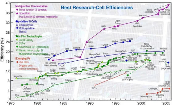
Now, we will review on the state of current and coming solar photovoltaic technology and their further development. Recent advances in concentrators, new directions for thin films, and materials/device technology issues are discussed in terms of technology evolution and progress. Insights to technical and other investments needed to tip photovoltaic to its next level of contribution as a significant clean-energy partner in the world energy portfolio [5]. The research progress over the past 25-30 years has been substantial and steady as shown in Figure 1.3.
developed and researched. Nanocrystal solar cells or quantum dot solar cells are solar cells based on a silicon substrate with a coating of nanocrystals. Quantum dot based photovoltaic cells based around dye-sensitised colloidal TiO2 films were investigated in 1991 [6] and were
found to exhibit promising efficiency of converting incident light energy to electrical energy, and were found to be incredibly encouraging due to the low cost of materials in the search for more commercially viable/affordable renewable energy sources. A single-nanocrystal (channel) architecture in which an array of single particles between the electrodes, each separated by ~1 exciton diffusion length, was proposed to improve the device efficiency [7] and research on this type of solar cell is being conducted by groups at Stanford, Berkeley and the University of Tokyo.
Recent research in experimenting with lead selenide (PbSe) semiconductor, as well as with cadmium telluride (CdTe), which has already been well established in the production of "classic" solar cells. Other materials are being researched as well. These materials are unlikely to have an impact in generating clean energy on a widespread basis, however, due to the toxicity of lead and cadmium.
On the other way, people effort to design ordered assemblies of semiconductor and metal nanoparticles as well as carbon nanostructures to utilize solar radiations. Dye sensitization of mesoscopic TiO2 has been widely used, and the power conversion efficiency up to 11% has
been achieved for such photochemical solar cells. Figure 1.4 depicts the assembled TiO2 and
CdSe quantum dots using bifunctional surface modifiers of type HS-R-COOH [8]. In additional, an ultrathin donor-acceptor solar cell composed entirely of inorganic nanocrystals has been introduced. This type solar cell is stable in air, and post-fabrication processing allows for power conversion efficiencies approaching 3% in initial tests. The photovoltaic devices described used rod-shaped CdSe and CdTe NCs as shown in Figure 1.5(a) and (b) [9].
1.3 Motivations
In previous works, the photo-sensing nanodevice composed of negative-charged Au nanoparticles and positive-charged CdSe/ZnS quantum dots has been developed and proposed [10]. However, there are several drawbacks or limits in previous design. For example, the solar cell efficiency is very low, and they have reliability and stability issues [11].
For the purpose of higher solar cell efficiency, the shorter length electrodes and different-sized QDs are applied in the proposed solar cell nanodevices based on “self-assembly technology.” Meanwhile, a low voltage, low drop-out regulator is designed to target the low power application and integrated with the proposed solar cell nanodevice. On other hand, to construct an equivalent circuit model of the proposed nanodevice is also one of the goals in the work.
1.4 Thesis Organization
In chapter 1, the background has been introduced in section 1.1, including the basic concepts, the definition, current trend of nanotechnology development in the world, and several assembly methods of NPs on silicon substrate. Then some reviews on the nanodevices and photovoltaic technologies in recent years have been discussed in section 1.2. At last, the motivations of this work and thesis organization are proposed in section 1.3 and 1.4.
In chapter 2, the fabrication technology will be discussed, including the process flow and the nanodevice structure design concepts. In section 2.1 and 2.2, the synthesis of Au NPs and PDDA-capped CdSe/ZnS QDs will be introduced. Then in section 2.3, the optical and electrical properties, including the mechanism of photoconductivity of PDDA-capped CdSe/ZnS QDs and the electron transportation between NPs will be demonstrated. In section 2.4, the design and fabrication flow of the advanced nanodevice structure will be proposed. And in section 2.5, the self-assembly process of Au NPs and PDDA-capped CdSe/ZnS QDs
will be discussed. And several reaction environment factors will be investigated in section 2.6. In chapter 3, the experimental results will be showed and discussed. First the measurement environment is introduced in section 3.1. Secondly the SEM images, optical and electrical properties, for example absorption / emission spectra of the proposed nanodeviced will be demonstrated in section 3.2. And then the nanodevice performance measurement will be showed and discussed in section 3.3. Next, an equivalent circuit model of the proposed nanodevice will be constructed in section 3.4.
In chapter 4, a low voltage, low drop-out linear regulator is designed to target the low power conditions and integrated with the proposed nanoparticle solar cell. In section 4.1, the system design considerations and relevant analysis will be introduced. The circuit blocks will also be showed in section 4.2. And then the simulation results and chip layout will be demonstrated in section 4.3. The proposed regulator system was successfully fabricated in TSMC 1P6M 0.18-μm CMOS process. Finally the measurement results will be showed and discussed in section 4.4.
Chapter 5 brings forth the conclusions of the research as well as implications thereof. Finally, the chapter ends with a few concluding statements pertaining to the research as well as recommendations for future work in the area.
Figure 1.1 Chemistry is the central science for further applications such as materials science and biotechnology. The combination of advanced materials and tailored biomolecules will produce the future nanodevices [1].
Figure 1.2 A gap currently exists in the engineering of small-scale devices. The top-down processes will have their limit below 100 nm, and the bottom-up processes will also have a limit at 2~5 nm. The gap will be filled by nanoclusters and biomolecules [1].
Figure 1.3 The efficiency evolution of best research cells by several of technology types. This figure identifies those cells that have been measured under standard conditions and confirmed at one of the word’s accepted centers for standard solar-cell measurements [5].
Figure 1.4 (a) Linking CdSe QDs to TiO2 particles with bifunctional surface modifier (HS-R-COOH); (b) Light harvesting assembly composed of TiO2 film functionalized with CdSe QDs on Optically Transparent Electrode (OTE) [8]. (Not to scale)
Figure 1.5 Transmission electron micrographs of (A) CdSe and (B) CdTe nanocrystals in ths investigation [9].
C
HAPTER
2
N
ANOPARTICLE
S
YNTHESIS AND
N
ANODEVICE
F
ABRICATION
T
ECHNOLOGY
In this chapter, the synthesis of Au nanoparticles and CdSe/ZnS quantum dots (QDs) will be discussed in section 2.1 and 2.2 respectively. And then the physical characteristics of the nanodevice will be demonstrated in section 2.3. In section 2.4, two kinds of electrode structures and nanodevice fabrication technology will be proposed. In section 2.5, the self-assembly process and experiment flow will be introduced. Finally, several reaction environment factors will be investigated in section 2.6.
2.1 The Synthesis of Citrare-Capped Au Nanoparticles
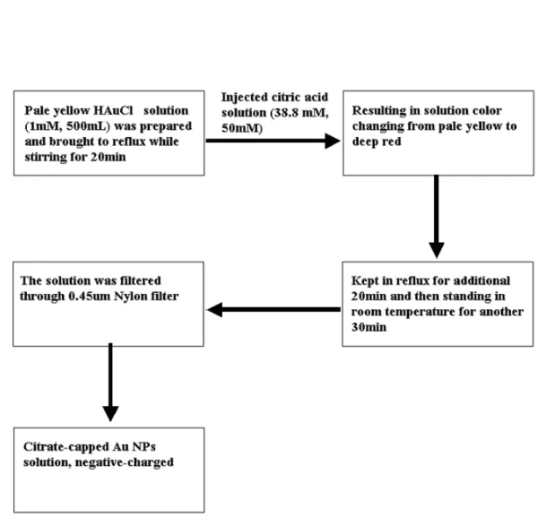
Au NPs with ~ 15 nm diameter were prepared by citrate reduction of HAuCl4 as
described in literature [12]. The pale yellow HAuCl4 solution (1 mM, 500 mL) was prepared
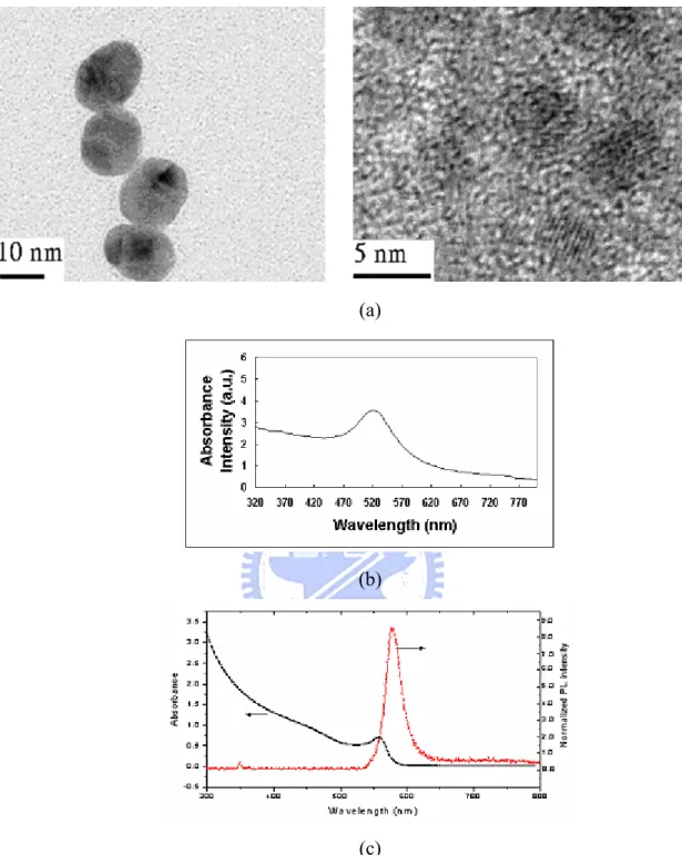
and brought to reflux while stirring for 20 minutes. A solution of citric acid (38.8 mM, 50 mL) was then quickly injected into the flask. The color of the solution changed from pale yellow to deep red indicating the formation of Au NPs. After color changing, the solution was kept in reflux for additional 20 minutes and then standing in room temperature for another 30 minutes. Finally, the solution was filtered through 0.45 μm nylon filter. The flow diagram of the Au NPs solution preparation is shown in Figure 2.1. The close photograph of the Au NPs solution is shown in Figure 2.2(a), (left). The TEM image of the approximately 15 nm diameter Au NPs is shown in Figure 2.3(a) and the UV-visible absorbance spectrum of Au NPs solution is shown in Figure 2.3(b).
2.2 The Synthesis of AET-CdSe and PDDA-CdSe Quantum Dots
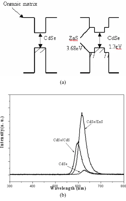
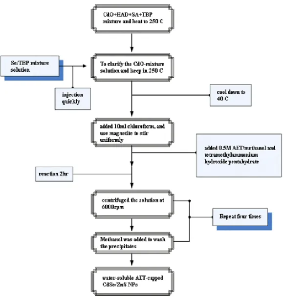
The emission efficiency, spectrum and time evolution of QDs are strongly affected by the surface. A better surface structure of QDs can provide higher stability, higher quantum yield and longer lifetime. Mostly the CdSe QDs lose a large portion of emission efficiency because of electron leakage resulting from the surface defect. Therefore, ZnS layer, a large band gap semiconductor, is used to passivate the surface and improve the quantum yield of CdSe NPs. The band gap diagram and the surface structures of CdSe/ZnS QDs are shown in Figure 2.4(a). It shows the PL intensity spectrum, which confirms the superior quantum yield property of CdSe/ZnS structure over the other two structures, CdSe and CdSe/CdS. The approximately 5 nm diameter fluorescent water-soluble ((PDDA)-coated) and (2-aminoethane thiol (AET)-coated) CdSe/ZnS QDs are supported from Prof. Yaw-Kuen Li’s laboratory, institute of molecular science, National Chiao Tung University, Taiwan. The surface of the AET-coated CdSe/ZnS QDs had positive-charged amino groups (-NH3+).z Synthesis of water-soluble AET-capped CdSe/ZnS QDs
In order to prepare positive charge on the QDs surface, the water stabilized amine terminating QDs (NP-NH2) was fictionalized. Adding methanol washed off the HDA
stabilizing layer and rendered a cloudy suspension which was centrifuged and the pellet containing QDs were washed with methanol 4 times to re-dissolve into chloroform. 1.0M 2-aminoethane thiol (AET) was added to the above solution and allowed to react for 2hrs. When ZnS capped CdSe QDs were reacted with AET, the mercapto group in AET bind to the Zn atoms and render the QDs hydrophilic, in addition to facilitating further functionalization possibilities. After the reaction, excess AET was washed off with methanol/chloroform mixed solution and store into the D.I. water.
(right). Figure 2.2(b) shows the close photographs of the mixture of 100 μL Au NPs solution and 100 μL AET-modified CdSe/ZnS QDs solution just after mixing (right), the mixture after standing 6 hrs (middle) in room temperature, and the mixture after standing 5 days in room temperature (left). As we can see, the color of mixture just after mixing was like that of Au NPs solution. However, after 6 hrs, it became dark purplish red. After 5 days, there was obvious precipitate at the bottom and the supernatant became pale yellow. The TEM image of the approximately 5 nm diameter CdSe/ZnS QDs is shown in Figure 2.3(a) and the UV-visible/PL spectra of CdSe/ZnS QDs solution is shown in Figure 2.3(c). The detailed modification processes of AET-capped CdSe/ZnS QDs are shown in Figure 3.5.
2.3 The Physical Characteristic of Au Nanoparticles and
CdSe/ZnS Quantum Dots
Recently, many nanoparticles (NPs) have been proposed and improved significantly. In order to achieve the nanodevices that have good performance, we must realize the electrical and optical properties as well as the size and the synthesis of the NPs. Metal particles comprise a fundamentally interesting class of matter in part because of an apparent dichotomy that exists between their sizes and many of their physical and chemical properties. For example, Au particles may be synthesized in diameters that span from the macroscopic down to the molecular scale (0.8 μm). Across almost the entire size regime, however, their electrical and optical behaviors are described with relatively simple classical equations, rather than the quantum mechanical concepts required understanding molecular entities. The classical free electron theory combined with optical constants for bulk gold is employed to successfully model the intense visible extinction of Au NPs. Moreover, the electrical and optical properties of metal particles can be tuned considerably simply by adjusting the size, shape, or extent of aggregation of the particles. For example, a typical solution of 13 nm diameter Au NPs is red
in color and exhibits a surface plasmon band centered at 518-520 nm. After aggregation, the extended polymeric Au NPs/polynucleotide aggregate shows a red to purplish blue color change in solution, due to a red shift in surface plasmon resonance of Au NPs [12]. The optical property of Au NPs is dominated by collective oscillation of conduction electrons resulting from the interaction with electromagnetic radiation. The electric field of incoming radiation induces the formation of a dipole in the NP. A restoring force in the NP tries to compensate for this, resulting in a unique resonance wavelength. The oscillation wavelength depends on particle size, particle shape and surrounding medium. [13]
In semiconductor nanocrystals, however, exhibit a wide range of size-dependent properties when the size regime is below 10 nm [14] [15]. Variations in fundamental characteristics ranging from phase transitions to electrical conductivity can be induce by controlling the size of the crystals [15]. There are two major effects to explain these size variation properties in nanocrystals. First, the number of surface atoms is a large fraction of the total atoms of a single nanocrystal. The high surface-to-volume ration will make a contribution to variations in thermodynamic properties of nanocrystals, such as melting point, and solid-solid phase transition. Second, nanocrystals with the same interior bonding geometry as the corresponding bulk material but with only a few hundred to thousand atoms exhibit dramatic size-dependent optical and electrical properties. These variations are because the density of states of electronic energy levels transforms as a function of the size of interior nanocrystal, known as quantization effects [15]. Nanocrystals lie in between the atomic and molecular limit of discrete density of electronic states and the extended crystalline limit of continuous bands.
The diagrams of density of states in metal and semiconductor nanocrystals are shown in Figure 2.6. In each case, the density of states is discrete at the band edges. The Fermi level is in the center of a band in a metal, and so kT will exceed the level spacing even at low temperature and small size. In semiconductor, however, the Fermi level lies between two
bands, so that the edges of bands dominate the low-energy optical and electrical behavior. Optical excitations across the gap depend strongly on the size, even for crystallites as large as 10,000 atoms. Besides, the HOMO-LUMO gap increases as the semiconductor nanocrystals become smaller (bellow 10 nm) [15].
In this work, we used positive-charged 2-aminoethane thiol (AET)-capped CdSe/ZnS (core/shell) NPs of approximately 5 nm in diameter as photoreceptors to detect lamination with above band gap photoexcitation [15]. We proposed two nanodevices composed of semiconductor QDs and/or metal NPs for self-assembly: (1) Au / AET-CdSe/ZnS. (2) Au / PDDA-CdSe/ZnS. However, some properties about CdSe QDs we must know that the exciton Bohr radius rb is the spatial extent of the electron hole pair in material and is defined as
2 * 2
b
4π
ε
m
e
r
=
h
(2.1)where ħ is the Plank’s constant, ε is the permittivity in bulk material, and m* is the effective mass. For CdSe semiconductor, the electron’s effective mass is 0.13 me and hole’s effective is
0.45 me. So the exciton Bohr radius of CdSe is calculated to be 4.9nm [14] [16]. If the
dimension of CdSe QDs is smaller than 4.9nm, the quantum confinement of electron hole pairs effects significantly. As size is reduced, the electron excitation shift higher energy, and there is concentration of oscillator strength into a few transitions [14]. The dynamic of the charge carriers in CdSe QDs have been in several reports. Monitored the electrons shuttling across the interface of CdSe QDs by femtosecond laser spectroscopy and showed that in CdSe QDs with no electron acceptors adsorbed on the particle surface, the excited electrons get trapped at the surface within 30 ps. Subsequently, electron-hole recombination takes place on a much longer time period > 10-7 s [17]. This is quite a useful knowledge for understanding the dynamics of electrons in CdSe QDs. The electrical transport properties of nanocrystals also depend strongly on size. On extended crystal, the energy required to add successive charges does not vary. In a nanocrystal, the presence of one charge prevents the addition of
another charge. Thus, in metal or semiconductor, the current-voltage curves of individual nanocrystal resemble a staircase, known as Coulomb blockade effect [15].
2.4 Nanodevice Fabrication Technology
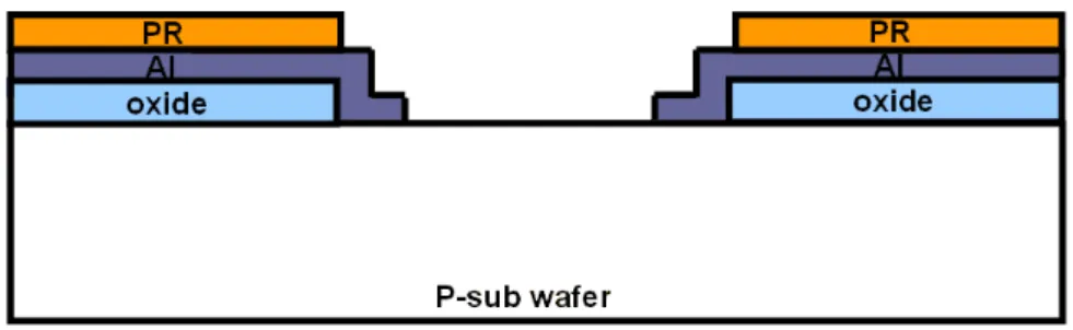
For the purpose of measuring and utilizing the power generated from the nanodevices, the electrodes are required. Hence, the electrodes were prepared before the self-assembly process. First, the nanodevice structure is introduced, and the cross-section is illustrated in Figure 2.7. The aluminum is used as the conductor to collect the current. And the oxide layer is utilized as the dielectric to prevent the substrate current flow to the aluminum in case of incorrect result when measuring.
However, in previous work, some problems were generated when the self-assembly process was executed. As the Figure 2.8(a) shown, according to the SEM photograph, some NPs and QDs assembled on unexpected region [11]. The anticipated patterns of the electrodes were disturbed by connecting with other electrodes through the thin film composed of NPs and QDs. This phenomenon may be caused by the presence of the –OH groups on the surface of the electrodes, which can be modified by TMSPED molecules, making them suitable sites for NPs assembly. In order to solve this problem, the lift-off technology was utilized to remove the unexpected NPs and QDs.
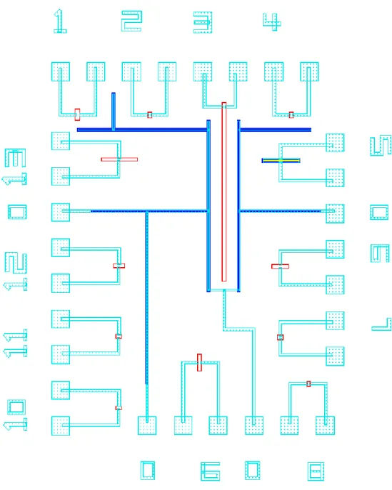
The proposed nanodevices were fabricated in National Nano Device Laboratory, Taiwan. The fabrication flow, including the self-assembly process which will be introduced in next section, is illustrated in Figure 2.9, and the corresponding mask layout view is shown in Figure 2.10. The dimensions of all nanodevices are list in Table 2.1.
On the other hand, it should be possible to further improve the performance of quantum dot solar cell by optimizing the light absorption properties of the nanostructure. Because semiconductor QDs such as CdSe with tunable band edge offer the opportunities to harvest
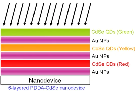
light energy in the entire region of solar light. One such approach under consideration is the construction of wideband solar cell, which employs an ordered assembly of PDDA-capped CdSe/ZnS QDs of different diameters. Smaller-sized QDs (larger band gap) absorb the portion of the light with smaller wavelengths (blue region). Light with longer wavelengths (red region), which is transmitted through the initial layer, is absorbed by subsequent layer, and so on. By creating an ordinary gradient of quantum dots of different sizes, it should be possible to increase the effective capture of incident light. Based on the above theorem and assumption, the nanostructure could be modified as shown in Figure 2.11. The upper layer is smaller-sized and the bottom layer is larger-sized PDDA-capped CdSe/ZnS QDs.
2.5 Self-Assembly Process for Advanced Nanodevice Structure
In previous chapter, we have discussed the forces that direct the assembly of NPs is similar to those involving in the interaction between molecules, such as hydrogen bonds, coulombic force, and van der Waal force. In this work, we utilize the coulombic force system control the assembly of NPs on the silicon or ITO glass. In coulombic force system, we take advantage of the positive or negative charge on the surface of NP to induce repulsion or attraction force between different NPs or between NPs and the substrate. The repulsion force will prevent the NPs from random aggregation before assembled on the substrate. Based on the coulombic force, we are able to construct the structure of advanced nanodevice on the silicon substrate effectively. The overall self-assembly process of Au NPs / PDDA-capped CdSe/ZnS QDs on the substrate by ionic interaction system is shown in figure 2.12.Now, the experiment flow will be introduced below. In order to modify the electrode surface with positive charges, the electrodes were immersed in 10% N-[3-(trimethoxysilyl)propyl]-ethylene diamine (TMSPED)/ deionized (DI) water solution over night to make the electrode surface provide amino groups (-NH3+) as the figure 2.12(a)
shown [18]. After immersion, the samples were cleaned by plenty of DI water to remove excess TMSPED staying on the surface, followed by dipping in dilute HCl solution for 3 seconds to protonate the amino groups. Finally, the samples were cleaned by using plenty of DI water for several times and dried. Subsequently, the TMSPED-modified samples were immersed in the citrate-capped Au NPs (~15nm) solution for 12 hours to make the negative-charged (-COO-) Au NPs self-assembly on the positive-charged (-NH3+) substrate by
ionic interaction. Therefore, Au NPs were coated on the entire substrate.
Next, the most important step of the experiment is to lift off the unexpected part where the Au NPs were on the photoresist. According to previous work, the acetone was used in lift-off process to dissolve the photoresist and brought out the substance attached to the photoresist as shown in Figure 2.12. And the acetone should not destroy the nanostructure [11]. Then the samples were immersed in the acetone for 5 minutes. The Au NPs on the photoresist were removed with the photoresist. After lift-off process the nanostructure is shown in Figure 2.13. And then, the samples were immersed in the Au NPs solution for 12 hours again to confirm if the Au NPs were coated with high density.
After 12-hour-immersion, the samples were cleaned by D.I. water for several times to remove free Au NPs and then immersed in PDDA-capped CdSe/ZnS QDs for 12 hours. So the positive-charged (-NH3+) QDs self-assembled to negative-charged (-COO-) Au NPs also
by ionic interaction. Theoretically, this process could be repeated for several times to form layers of closed packed PDDA-capped CdSe/ZnS QDs and Au NPs nanostructures. As a result, this nanostructure can be used as the photovoltaic nanodevice. The experimental results will de discussed in the next chapter.
2.6 Reaction Environment Investigation
There are several environmental factors which would have effects on the nanostructure, for example, reaction temperature and reaction time. These effects should be optimized.
Accordingly, some experiments to affirm the optimum reaction conditions for the nanodevices to fabricate were executed first.
As a matter of fact, to construct the nanostructure is like to build the building. The base of the nanostructure should have higher density. Therefore the first layer, Au NPs, plays an important role in self-assembly process. If the density and quality of the first Au NPs thin film is high, the second and subsequent layers would also get high.
Hence, two experiments were executed. One is to observe the reaction time effect on the nanostructure construction. The other is to investigate the reaction temperature effect. And then SEM photograph of the nanodevices helps us to determine which conditions are suitable. In previous work, an experiment was to investigate the temperature effect on the nanostructure construction. Hence, two pieces of p-type silicon wafer was prepared. One was to be coated with Au NPs and PDDA-capped CdSe/ZnS QDs as a 2-layer basic nanostructure in the room temperature environment. The other was to be coated in the same way, but in the 4°C reaction environment. Figure 2.16 shows the experiment outcomes. As the Figure 2.14(a) shown, the nanostructure which was constructed on condition of the room temperature got lower density.
The other experiment is to observe if the different reaction time influence the nanostructure. Therefore, two pieces of quartz glasses were prepared. One was to be coated with Au NPs and PDDA-capped CdSe/ZnS QDs as a 4-layer basic nanostructure for 4 hours per layer. The other was to be coated in the same way, but 12 hours per layer reaction period. The result is shown as Figure 2.15. Figure 2.15(a) is the nanostructure that was fabricated with 4 hours reaction time per layer. Figure 2.15(b) is the nanostructure that was constructed with 12 hours reaction time per layer. As a result, the 12-hour-reaction-time one got high particle density. It benefits the nanodevice construction.
In conclusion, lower temperature and longer reaction period would benefit nanostructure. Therefore, these two factors would be adopted in the nanodevice fabrication technology.
Table 2.1 The dimensions of all horizontal electrodes fabricated in NDL are list in this table. (unit:μm)
Pad Description
Pad_7 Pad_8 Pad_10 Pad_11 5x30 0.5x30 1x30 2.5x30
Figure 2.2 (a) The close photographs of 100 μL of approximately 15 nm diameter Au NPs solution + 100 μL DI water (left) and 100 μL of approximately 5 nm diameter AET-CdSe/ZnS NPs solution + 100 μL DI water (right). The Au NPs solution was in deep red while the AET-modified CdSe/ZnS NPs solution was in yellow. (b) The close photographs of the mixture of 100 μL Au NPs solution and 100 μL AET-modified CdSe/ZnS NPs solution just after mixing (right), the mixture after standing 6 hrs (middle) in room temperature, and the mixture after standing 5 days in room temperature (left). As we can see, the color of mixture just after mixing was like that of Au NPs solution. However, after 6 hrs, it became dark purplish red. After 5 days, there was obvious precipitate at the bottom and the supernatant became pale yellow.
(a)
(b)
(c)
Figure 2.3 (a) The TEM image of Citrate-capped approximately 15 nm diameter Au NPs and the TEM image of AET-capped approximately 5 nm diameter CdSe/ZnS QDs. (b) The UV-visible spectrum of Au NPs solution. (c) The UV-visible and PL intensity spectrum of AET-CdSe/ZnS QDs solution.
(a)
(b)
Figure 2.4 (a) The band gap and surface structure diagram of CdSe/ZnS QD. (b) The PL intensity spectrum of different kind of surface capping method of CdSe QD
Figure 2.6 Density of states in metal (A) and semiconductor (B). In each case, the density of states is discrete at the band edges. The Fermi level is in the center of a band in a metal, and so kT will exceed the level spacing even at low temperature and small size. In semiconductor, the Fermi level lies between two bands, so that there is large level spacing even at large size. The HOMO-LUMO gap increases as the size of semiconductor nanocrystal decreases (bellow 10 nm). [11].
Figure 2.7 The cross-section view of the electrode structure and the PR is photoresistor for lift-off process.
(b)
Figure 2.8 (a) The cross section figure of the electrodes structure corresponds to SEM image of the nanodevice-modified silicon chip. (b) The current flow trend of the nanodevice structure, and the electrodes dominated the source of the generated current. In the worse case, the whole chip area is considered, not the area of the electrodes. (The twill line means the thin film structure composed of NPs and QDs.).
(a) (b) (c) (d) (e) (f) (g) (h)
(h) (j) (k) (l) (m) (n)
Figure 2.9 Fabrication flow of the proposed nanodevice (top-view and cross-section view). From (a) to (j) is the electrode fabrication process, and (k) to (n) is the nanostructure self-assembly (SAM) process.
Figure 2.10 The corresponding mask layout view. There are six masks in this work, and all details are list in Table 2.1.
Figure 2.11 The cross-section view of modified nanostructure with Au NPs and three different-sized PDDA-capped CdSe/ZnS quantum dots. The bottom layer is composed of larger-sized QDs (smaller band gap, absorb smaller wavelength), and the top layer is composed of smaller-sized QDs (larger band gap, absorb longer wavelength). This is because light with longer wavelengths (ref region) is transmitted through initial layer.
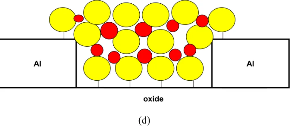
oxide Al O O O Si NH2+ NH3+ O O O Si NH2+ NH3+ Al (a) oxide Al O O O Si NH2+ NH3+ O O O Si NH2+ NH3+ Al COO -COO -COO -COO -COO -COO -(b) oxide Al NH3+ Al COO- COO- COO- COO
-NH3+ NH3+ NH3+ NH3+ NH3+ NH3+ NH3+ (c)
oxide
Al Al
(d)
Figure 2.14 The fabrication process of the nanostructure by coulombic force system after lift-off process. (a) The modification of TMSPED on the silicon oxide surface and the protonation of amino (-NH3+) groups, (b) The assembly of ~ 15 nm diameter Au NPs on silicon oxide substrate by ionic interaction, (d) The assembly of ~ 5 nm diameter AET-CdSe/ZnS NPs on the silicon oxide substrate by ionic interaction, and (e) The formation of the photo-sensing nanodevice structures after repeated assembly process. (Not to scale)
Figure 2.15 SEM photograph of nanodevice with lift-off process, the black part is the place where Au NPs and CdSe QDs deposit.
(a) (b)
Figure 2.16 The temperature effect on the nanostructure (SEM photograph). (a) the nanostructure constructed at room temperature (b) the nanostructure constructed at 4°C environment.[11]
(a) (b)
Figure 2.17 The reaction time effect on the nanostructure (SEM photograph). (a) the nanostructure with 4-hour-reaction time per layer (b) the nanostructure with 12-hour-reactime per layer
C
HAPTER
3
E
XPERIMENTAL
R
ESULTS AND
D
ISCUSSIONS
3.1 The Environment Setup for Measurement
At first, Figure 3.1(a) shows the photographic of the electrodes of the nanodevice fabricated in NDL. And Figure 3.2(b) demonstrates the enlarged view of one nanodevice. After fabrication, the nanodevice were observed and evaluated by using scanning electron microscopy (SEM) photographs.The SEM was performed with JSM-6500F high-resolution scanning microscope. In this work, daylight lamp and laser diode are used as illumination light source. The environment setup for I-V characteristics measurement is shown in Figure 3.2. The laser diode driver is PicoQuant POL 800D and the 375 nm laser diodes are PicoQuant LDH-P-C375. And I-V characteristic measurement instrument is HP 4156.
On the other hand, the specific optical characteristics of the nanostructure are confirmed by UV-visible and Photoluminescence (PL) spectra. The UV-visible absorption spectrum analysis is performed with Hitachi-U-3010 Spectrophotometer. The detecting wavelength is in the range from 190 nm to 1000 nm. The typical experimental setup is shown in Figure 3.3. A beam of light from a visible and/or UV light source (red colored) is separated into its component wavelengths by a prism or diffraction grating. Each monochromatic (single wavelength) beam in turn is split into two equal intensity beams by a half-mirrored device. One beam, the sample beam (colored magenta), passes through a small transparent container (cuvette) containing a solution of the compound being studied in a transparent solvent. The other beam, the reference (colored blue), passes through an identical cuvette containing only the solvent. The intensities of these light beams are then measured by electronic detectors and
compared. The intensity of the reference beam, which should have suffered little or no light absorption, is defined as I0. The intensity of the sample beam is defined as I. Over a short
period of time, the spectrometer automatically scans all the component wavelengths in the manner described. The ultraviolet (UV) region scanned is normally from 200 to 400 nm, and the visible portion is from 400 to 800 nm. If the sample compound does not absorb light of a given wavelength, I = I0. However, if the sample compound absorbs light, I is less than I0.
And this difference may be plotted on a graph versus wavelength. Absorption may be presented as transmittance (T = I/I0) or absorbance (A = log I0/I). If no absorption has
occurred, T = 1.0 and A = 0. Most spectrometers display absorbance on the vertical axis, and the commonly observed range is from 0 (100% transmittance) to 2 (1% transmittance). The PL spectrometer analysis is performed with Jobin Yvon Instrument S. A. Inc. Spectrometer. The scanning range is from 200 nm to 1000 nm. The typical experimental setup for PL intensity spectrum measurement is shown in Figure 3.3. When light of sufficient energy is incident on a material, photons are absorbed and excite the electrons from ground state. If radiative relaxation occurs, the emitted light is called photoluminescence (PL). This light can be collected and analyzed to yield a wealth of information about the photo-excitation nanostructure. In this experiment, we used laser source with different wavelengths to photo-activate the nanostructures. Subsequently, the emitted light was passing through a filter lens that can filter out the wavelengths < 500 nm, then analyzed by spectrometer and got into a photo-detector. Eventually, the PL signal data are recorded into computer.
3.2 SEM Images And Optical Absorption / Emission Spectra
The SEM images of the surface of SiO2/Si quartz fragments after repeated
self-assembly process are shown in Figure 3.5. And through Figure (a) to (e), Au NPs and PDDA-capped CdSe/ZnS QDs were successfully deposited on the quartz. As we can see in
the images, the nanostructure became more and more compact while increasing the number of layers step by step. Besides, for Au NPs / PDDA-capped CdSe nanostructure, after multi-layered structure was formed, typically more than 3 layers, the gold color shining can be easily observed by naked eye. First, the sample (electrode) was modified by N-[3-(trimethoxysilyl)propyl]-ethylene diamine (TMSPED), which provided positive-charged amino (-NH3+) groups to attract negative (-COO-) charged Au. Second, the
modified PDDA-capped CdSe/ZnS QDs that had positive-charged amino groups on the particle surface were assembled on Au NPs. Theoretically, the assembly process can be repeated for several times to form multi-layered nanostructure of PDDA-capped CdSe/ZnS QDs and Au NPs. And then figure 3.6 shows the lateral SEM photographic of the nanodevice. The surface of the nanostructure is not smooth, since PDDA is capped the surface of CdSe/ZnS QD.
Furthermore, in order to prove that the closely packed nanostructure has superior optical properties, we observed the UV-visible and Photoluminescence (PL) intensity spectra of the different-sized PDDA-capped CdSe/ZnS quantum dots solution. From the absorption spectrum, we can see that the peak of absorbance was about 500nm ~ 600nm, as shown in Figure 3.6. Besides, the nanostructure retains the optical characteristics of CdSe QDs when they are bound to each other, which can be verified by identifying the characteristic absorbance peaks of Au NPs (~520 nm) and CdSe QDs (~580 nm) in the spectrum. However, in some cases, we observed the peaks of Au NPs (~520 nm) and CdSe QDs (~580 nm) are so close that they merge to form a board band in the spectrum for Au / CdSe nanostructure as shown in figure 3.7.
The PL intensity spectra of different-sized PDDA-capped CdSE/ZnS QDs were shown in figure 3.8. When we used 365 nm wavelength for optical excitation, there were three peaks, red, yellow and green respectively, as shown in figure 3.8. It means that different-sized quantum dots have different optical properties, and figure 3.9 shows the
photography of different-sized PDDA-capped CdSe/ZnS QDs. We can utilize these characteristics to design an order assembly multi-layer nanoparticles or quantum dots thin films to realize high-efficiency solar cell. However, during the dip-and-wash procedure, the instable bond between the NPs and QDs will cause the existence of defect. So the probability of defect will be reduced when the number of layers increases.
3.3 Nanodevice Performance Measurement
I-V characteristics of the proposed nanodevices are measured in this section. The measurement environment was introduced in the section 3.1. And the electrode sets we used, 30 μm / 5 μm, 30 μm / 2.5 μm, 30 μm / 1 μm, and 30 μm / 0.5 μm (width / length). After the fabrication process described in Section 2.4, the I-V measurement was performed by applying voltage biases to the electrodes and measuring the current flowing through the nanodevice while in dark or under 0.16mW / cm2 daylight lamp illumination. The result of the nanodevice is shown as Figure 3.10 and 3.11. It is a resistive device in dark. After illumination, the photocurrent is generated. It is also linear but a y-axis direction shift. And then the shift quantity is the photocurrent.
According to the experimental results, the photocurrent was increased as the length of the nanodevice decreased. Therefore, the photocurrent volume density (PVD) was also increased as the length decreased. Another important specification of the nanodevice is the open-circuit voltage, and it increased as the length of the nanodevice decrease. And the most important specification is the solar cell efficiency because it remarks the performance of the nanodevice. All experimental and measurement results are list in Table 3.1. Figure 3.12 (a) (b) (c) (d) and (e) show the relation between the photocurrent, open-circuit voltage, PVD, power volume density, efficiency and length of the proposed nanodevice. And above figures demonstrate the error bar of the experimental results. As Figure 3.13 shown, after
24 days the performance of the nanodevice decayed. This phenomenon may result from destruction of nanostructure. Because these samples were not stored in a dry environment, the humidity or oxidation would decrease the reliability. However, after 26 days, the decay tended to saturate.
In this work, under the 0.16 mW/cm3 illumination, the best solar cell efficiency is 1.6% (6-layered PDDA-capped CdSe/ZnS nanodevice with 60 μm in width and 0.5 μm in length). The maximum photocurrent is 664.62 pA. Then, the maximum photocurrent volume density (PVD) is 7.385×10⁻¹⁹ A/nm3 and power volume density is 4.256×10⁻²² W/nm3. Finally, table 3.2 compares the measurement results of this work and previous works [12].
3.4 Nanoparticle Solar Cell Efficiency Estimation and Nanodevice
Model Construction
Figure 3.14(a) depicts the traditional p-n junction solar cell, and its I-V curve is shown in Figure 3.14(b). According to this I-V characteristic, an effective circuit model of p-n junction solar cell model is illustrated in Figure 3.14(c), where Rs is a small seris resistor and Rp is a
very large parallel resistor. In this work, a resistive load is connected to the solar cell. Therefore, an operation point is obtained as shown in Figure 3.15. And the parameter, fill factor is defined. sc oc m m I V I V factor fill ⋅ ⋅ = , (3.1)
where Voc is the open circuit voltage of the solar cell. Isc is the short current of the solar cell.
Vm and Im is the voltage and the current when the product of the voltage and current (power)
is maximum. Then, the efficiency can be defined as factor fill P I V Efficiency in sc oc⋅ × = , (3.2)
where Pin is the power of the incident light source. Now, we could define the formula of I-V
curve and estimate its maximum power.
sc sc V I V I I= ⋅ + oc ⎟⎟ ⎠ ⎞ ⎜⎜ ⎝ ⎛ + ⋅ = × = ∴ sc V Isc V I V I V Power oc 0 I V V 2I V Power Let = sc ⋅ + sc = ∂ ∂ oc cell solar of power maximum a is there , 2 I I , 2 V V= oc = sc ⇒ ( ) V I 2 41 I 2 V I V I V factor fill sc oc sc oc sc oc m m max ⋅ = ⋅ = ⋅ ⋅ = (3.3)
Based on the conventional p-n junction equivalent circuit model, the proposed Au NPs/ PDDA-capped CdSe/ZnS QDs nanodevice model could be constructed. An Au NP and a PDDA-capped CdSe/ZnS QD could be considered as a micro p-n junction solar cell or nano-schottky diode. As shown in Figure 3.16(a), there is a unit cell of the nanodevice between Au NPs and PDDA-capped CdSe/ZnS QD. Figure 3.17 depicts the 1-demensionan nanodevice model. It is a symmetrical structure. And Rs1 and Rs2 are small series resistors, Rp1
and Rp2 are very large parallel resistors. I1 and I2 are the photocurrent after illumination.
For HSPICE simulation, the metal-insulator-semiconductor diode model is employed. And then 2-dimension and 3-dimension nanodevice models could also be constructed in similar way. Figure 3.18 and 3.19 illustrate the 2-dimension and 3-dimension nanodevice equivalent circuit model respectively.
It is worth mentioning that 3-dimension nanodevice model is more complicated than 1-D and 2-D model. Figure 3.19 depicts the ideal 3-dimension nanostructure. The unit cells connect two of the 2-D nanodevice model to form a 3-D nanodevice model. The simulation parameters illustrate in Figure 3.20. First, for HSPICE simulation, Metal-Insulator-Semiconductor diode model was employed. X-dimension unit cell : Rs=15kΩ, Rp=7MΩ, I=2.1nA; Y-dimension unit cell : Rs=0.918MΩ, Rp=289MΩ, I=2.1nA,