國
立
交
通
大
學
電子工程學系 電子研究所
博 士 論 文
前瞻非揮發性奈米點記憶體元件之製作與特性研究
Fabrication and Electrical Characterization of Advanced
Nanocrystals Nonvolatile Memories
研 究 生:陳緯仁
指導教授:張俊彥 院士
前瞻非揮發性奈米點記憶體元件之製作與特性研究
Fabrication and Electrical Characterization of Advanced
Nanocrystals Nonvolatile Memories
研 究 生:
陳緯仁
Student:Wei-Ren Chen
指導教授:
張俊彥 院士
Advisor:Dr. Chun-Yen Chang
國 立 交 通 大 學
電子工程學系 電子研究所
博 士 論 文
A Dissertation
Submitted to Department of Electronics Engineering and Institute of Electronics
College of Electrical and Computer Engineering National Chiao Tung University
in partial Fulfillment of the Requirements for the Degree of
Doctor of Philosophy in
Electronics Engineering
October 2008
前瞻非揮發性奈米點記憶體元件之製作與特性研究
研究生: 陳 緯 仁 指導教授: 張 俊 彥 院士
國 立 交 通 大 學
電子工程研究所
摘 要
目前非揮發性記憶體在元件尺寸持續的微縮下,其需求為高密度記憶單 元、低功率損耗、快速讀寫操作以及良好的可靠度(Reliability)。然而傳統浮動閘 極(Floating gate)記憶體在操作過程中,穿遂氧化層產生漏電路徑會造成所有儲存 電荷流失回到矽基版,隨著尺寸微縮這種情況會更糟,所以在資料保存時間 (Retention)和耐操度(Endurance)的考量下,微縮穿遂氧化層的厚度是非常困難 的。具非揮發性奈米點記憶體及 SONOS 記憶體被提出並希望可取代傳統浮動閘 極記憶體,由於彼此分離的儲存點作為儲存中心,所以上述兩者可以有效改善小 尺寸記憶體元件多次讀寫操作下的資料儲存能力。 在本論文中,主要提出三種不同性質的奈米點(鍺、矽化鎳與錳矽氧化物奈 米點)材料來克服傳統非揮發性記憶體在微縮過程中會遭遇到的困難,我們首先 提出一種矽鍺氧薄膜的堆疊結構作為鍺奈米點的自我析出層(Self-assembled layer),並應用在奈米點非揮發性記憶體上。在室溫環境中,利用濺鍍(Sputtering) 矽鍺(Si0.5Ge0.5)混合靶材的方式來形成電荷儲存層,同時加入氬氣及氧氣一起共 鍍,此方式可以成功的將氧氣原子摻入至矽鍺中形成矽鍺氧三元結構的薄膜,另 外,在我們的實驗中,我們也發現在氮氣熱退火之前先疊加上一層氧化矽作為阻 擋鍺揮發的阻擋層,此為使用矽鍺氧薄膜作為電荷儲存層的一個關鍵步驟。之後 我們再利用氧、矽與鍺之間不同氧化競爭的現象,經由快速熱退火製成來形成均勻且高密度(~1012 cm-2)的鍺奈米點埋藏於氧化層中。此鍺奈米點製程相對於傳統 鍺奈米點製作,可以有效地防止鍺被過度氧化並且降低電荷儲存效率。同樣地, 我們運用類似的鍺奈米點形成機制,在濺鍍的過程中將氧氣置換成氮氣,利用同 樣的方式製作鍺奈米點且奈米點可以在析出過程被包覆在氮化矽(SiNx)的結構 中,其記憶窗口比先前的鍺奈米點埋藏在氧化矽結構還顯著,此乃因為鍺奈米點 埋在氮化矽為主的電荷儲存層裡,會與奈米點周圍的介電層產生額外的電荷儲存 中心,進而增加記憶體整體效能,另外,我們比較這兩種結構的鍺奈米點記憶體, 由於氮化矽能使儲存電荷均勻分佈於儲存層以降低庫倫斥力效應,所以在本研究 中不論在電荷儲存能力與可靠度上,埋藏在氮化矽的鍺奈米點記憶體都展現較好 的記憶體特性。 近年來已經發展了許多方法來形成奈米點記憶體,一般而言,大多數的方 法都需要長時間且高溫的熱退火製程,這個步驟會影響現階段半導體製程中的熱 預算和產能。因此在本論文中,我們使用一個簡單、低溫的製程方法來形成鎳氧 矽化物(Ni-O-Si)和鎳矽氮化物(Ni-Si-N)奈米點,並將其應用於非揮發性記憶體元 件上。我們一樣在氬氣和氧氣(Ar/O2)的環境中濺鍍混合鈀材 Ni0.3Si0.7形成氧化 矽(SiOx)包覆著鎳氧矽化物(Ni-O-Si)的非揮發性記憶體結構,我們認為在此濺鍍 過程中會形成奈米點結構,氧氣扮演一個不可或缺的角色,可以簡單並均勻地形 成高密度(~1012 cm-2)的奈米點分佈。我們同時也提出室溫下在氬氣和氮氣(Ar/N2) 的環境中濺鍍混合鈀材 Ni0.3Si0.7來形成鎳矽氮化物(Ni-Si-N)奈米點,結果也可發 現高密度鎳矽氮化物奈米點被包覆在氮化矽(SiNx)中,並且擁有更好的儲存能
力。因此我們利用這些元素之間的不同吉布斯自由能(Gibbs free energy)來產生一 個內部競爭機制,可以在較低溫的環境中形成所謂的低溫化的非揮發性金屬奈米 點記憶體。 我們進一步利用一個500°C~600°C的快速熱退火製程,藉由鎳與矽的化合反 應來增進奈米點的結晶性(Crystallization),矽化鎳(NiSi)金屬奈米點會因此形成 並且擁有較高的態位密度(Density of state)來儲存電荷並增加記憶窗口與儲存電 荷穩定性;因為熱退火處理也可以改善氮化矽本身的品質與減少奈米點周圍氮化 矽中的淺層缺陷(漏電路徑),記憶體的可靠度同時也被有效率地改善。因此我們
藏於不同介電層中的電場結構模擬,與氧化矽包覆的金屬奈米點相較之下,由於 不同介電質中具有不同的電場分佈,氮化矽包覆奈米點作為電荷儲存層有較佳的 可靠度表現。最後我們製作多層的矽化鎳奈米點記憶體結構並探討其特性,發現 多層奈米點比單層奈米點不僅在室溫下且在高溫時也擁有較好的電荷儲存能力 和保存能力,此乃因為多層奈米點的第一與第二層因尺寸所產生的量子侷限效應 (Quantum confinement effect),可以加以阻擋第三層的主要儲除電荷的流失路徑。
再者,針對介電質奈米點記憶體,我們也使用濺鍍系統形成錳矽氧化物 (MnSiOx)奈米點,且進一步利用X光光電能譜(XPS)鑑別錳矽氧化物奈米點的組 成以及能隙與能帶圖的建立。並藉由量測電流密度與溫度的關係,使用缺陷輔助 穿隧模型來萃取錳矽氧化物的缺陷深度與密度,進而可以發覺氧原子的摻雜濃度 會影響缺陷深度,使得電荷保持能力會有所差別。我們也製作雙層錳矽氧化物 (MnSiOx)奈米點記憶體結構並探討其特性,可以發覺其比單層的介電層奈米點有 較好的電荷儲存特性與保持能力,此乃因為介電層奈米點的電荷儲存方式是藉由 自身的缺陷捕獲所致,所以已被捕獲的電荷必須先克服介電質奈米點的缺陷能 障,方能逃脫出奈米點並流失掉。最後,我們所提出的奈米點結構與製造技術都 可以應用於非揮性奈米點記憶體的製程技術同時也適用於現階段積體電路製程。
Fabrication and Electrical Characterization of
Advanced Nanocrystals Nonvolatile Memories
Student: Wei-Ren Chen Advisors: Prof. Chun-Yen Chang
Department of Electronics Engineering and Institute of Electronics
National Chiao Tung University, Hsinchu, Taiwan
Abstract
Current requirements of nonvolatile memory (NVM) are the high density cells, low-power consumption, high-speed operation and good reliability for next-generation NVM application. However, all of the charges stored in the floating gate will leak into the substrate if the tunnel oxide has a leakage path in the conventional NVM during endurance test. Therefore, the tunnel oxide thickness is difficult to scale down in terms of charge retention and endurance characteristics. Nanocrystals (NCs) NVMs are one of promising candidates to substitute for conventional floating gate memory, because the discrete storage nodes as the charge storage media have been effectively improve data retention for the scaling down device.
In this thesis, we propose three kinds of NCs with different properties (Ge, NiSi and MnSiO NCs) to overcome the limitation of conventional NVMs during the
NCs self-assembled layer for application of NCs NVMs. We successfully incorporated the oxygen atoms into SiGe layer to form a SiGeO ternary film by sputtering a commixed Si0.5Ge0.5 target in an Ar/O2 ambiance at room temperature. In
this work, we fond out that pre-annealing-capping oxide (PACO) is a critical step in our experimental process, and the charge storage layer can be used the different oxidized competition mechanism between Si and Ge to form Ge NCs embedded in oxide. Hence, a uniform and high density (~1012cm-2) of Ge NCs was fabricated after a rapid thermal annealing (RTA) process. Our propose technique compared with traditional Ge NCs process can be efficiently to prevent the over-oxidation phenomenon of Ge NCs which reduces the charge trapping ability. Furthermore, we also used this similar method that oxygen was replaced by nitrogen to form the Ge NCs embedded in SiNx structure. The memory window for the stacked structure with
Ge NCs embedded in SiNx layer was larger than Ge NCs embedded in SiOx layer, due
to the extra charge trapping centers generated from the surrounding dielectric of Ge NCs. To compare these Ge NCs structures, we found that the Ge NCs embedded in nitride had better charge storage ability and reliability for NVM characteristics, because the nitride layer can uniformly distribute the stored charge to reduce Coulomb repulsive force effect under retention test.
In recent years, most methods of NCs fabrication generally need the thermal treatment with high temperature and long duration. This procedure will influence thermal budget and throughput for the current manufacture technology of semiconductor industries. Hence, an ease and low temperature fabrication technique of Ni-O-Si and Ni-Si-N NCs was demonstrated for NVM application in this thesis. The NVM structure of Ni-O-Si NCs embedded in the SiOx layer was fabricated by
sputtering a commixed target (Ni0.3Si0.7) in an Ar/O2 environment at room temperature.
NC formation. In addition, a high density (~1012cm-2) NCs also can be simple and uniform to be fabricated in our study. We also proposed a formation of Ni-Si-N NCs by replacing O2 by N2 environment during the sputtering process. It was also found
that a high density Ni-Si-N NCs was embedded in the silicon nitride (SiNx) which
presented larger memory effect. Therefore, by using this internal competition mechanism of charge trapping layer for these elements (Ni, Si, and O/N), we can obtain a metallic NCs NVM with low temperature process.
A RTA process with temperatures about 500 and 600 °C at short duration was further used to improve the crystalline quality of metallic NCs and its memory reliability. Thermal treatment can efficiently reduce the defects (leakage path) in the SiNx which surrounds the nanocrystal. The charge storage layer of NCs embedded in
SiNx shows larger memory window and better reliability over NCs embedded in SiOx,
due to different distributions of electronic field in the NC and surrounding dielectric by the simulation results. In addition, multi-layer NiSi NCs NVM structure had better charge storage and retention over than single-layer metal nanocrystals under high temperature test, because of the first and second layer of multi-layer with Quantum confinement effect depended by the NC size.
For dielectric NCs NVMs, we also used the sputter system to fabricate the manganese silicate (MnSiOx) NCs. The XPS results of charge trapping layer can be
identified the chemical state of NCs and built the energy band diagram of our produced MnSiOx thin film. Moreover, by the relationship of current density with
temperature, the trap assisted tunneling model can be used to extract the charge trapping level and density of MnSiOx. In the experiment results, the oxygen doping
concentration will affect the trap level positions and also influence the retention presentations for the reliability test. Moreover, double layer MnSiOx NCs NVM also
and keeping charges ability than single layer because the trapped charges must overcome the trap barrier and then escape from NCs due to the trapping mode of dielectric NCs.
Key words: Nanocrystal, SONOS type, Nonvolatile memory, Ge, NiSi, MnSiO,
Acknowledgement
四年的研究所回憶歷歷在目,終於順利完成博士學位,從碩士直接攻讀博士 需要要很大決心與毅力,這期間我要感謝我的指導教授張俊彥院士給我許多在研 究觀點上的看法與指導,讓我能擁有獨立思考與克服困難的能力,也時時教授我 做人處事應該有的胸襟與看法,才能使我如此快速的成長。也要感謝中山大學的 張鼎張教授,於大學時代即帶我進入這個領域並建立我的基礎能力與知識,讓我 能於後續的研究過程中適時發揮,也在我遭遇瓶頸階段給予充分的鼓勵與建議, 協助我能一步步的將這個學位完成,在此再次用感恩的心感謝所有指導過我的老 師以及所有提供我研究資源的機構。 研究所生涯有許多點點滴滴,這些也是助我成長的原動力,首要感謝伴我度 過研究所生活的學長們,有紀文、炳宏、宗熺、峻豪與世青學長,有你們的無私 的經驗傳授,我才能開拓知識,感謝清大的俊文與偉鑫學長,沒有你們的 TEM 幫助,這本博士論文將會難產,感謝 418 的兆欽、怡誠學長與心卉學姐,有你們 的扶持幫忙我才能這麼快取得學位,也要感謝一路伴我的同學與學弟妹,有柏 舜、阿貴、小馬、睿龍與貴宇,這本博士論文也是你們的辛苦結晶,我想與你們 共享,以及星舟、家瑋、佳州、勝凱(承恩)、志晟、仕承與俐婷,感謝你們在我 直攻那年帶給我歡笑並見識到什麼是男人的豪氣,還有陳董、立偉、昭正與志瑋, 感謝你們將 521 與實驗室其他學弟妹都帶領的有聲有色的,替我分擔很多忙。另 外,我要感謝哲榮、詩國、峻丞、成能、方方土、述穎、勝杰、大頭、狗哥、聖 齊與逸立,你們總是帶給實驗室歡樂的氣氛,也要感謝新進的學弟,信淵、耀峰、 誌陽與培維,感謝你們在口試的張羅與實驗室的打點。 在此特別感謝中山的夥伴們,有富彥、書瑋、崎峰、原瑞、柏均、佳盛、敏 甄、一精、正杰、冠張、書慶、漢博與志豪等其他學弟妹,我懷念在中山與你們 一起做實驗的時光與辛酸,感謝你們讓我在中山能有一個美好的回憶。也感謝我 女友的實驗室學弟妹,建佑、綿綿、阿輝與雲漢,謝謝你們為我提供寫作的空間與資源成就這本論文的第一刷。 最後要感謝我摯愛的女友,李柳萱小姐,伴我度過研究所期間的每一刻, 在每個重要時刻都為我打氣加油祝福,讓我順利度過難關,往後也將是如此,妳 是我人生中不可或缺的一部分。這本論文我要將其獻給我親愛的家人,陳國欽先 生與蘇惠屏女士,你們是我人格養成的重要推手,讓我求學生涯無後顧之憂的 人,也是我人生中最重要的避風港,我信心的泉源,你們是我人生中的支柱,我 將這份喜悅獻給我的家人。 秋分 緯仁 2008.10.於新竹交大
Contents
Chinese Abstract---
IEnglish Abstract---
VIAcknowledgement---
VIIIContents---
XTable Captions---
XIIIFigure Captions---
XIVChapter 1 Introduction
1.1 Overview of Nonvolatile Memory---1
1.1.1 SONOS Nonvolatile Memory Devices---3
1.1.2 Nanocrystal Nonvolatile Memory Devices---6
1.2 Motivation---11
1.3 Organization of This Thesis---12
Chapter 2 Basic Principles of Nonvolatile Memory
2.1 Programming/Erasing mechanisms of nonvolatile memory---172.1.1 Tunneling effect---18
2.1.2 Channel Hot-Electron Injection (CHEI)---22
2.1.3 Band to Band Tunneling (BTBT)---25
2.1.4 Channel Initiated Secondary Electron Injection (CHISEI)---27
2.2 Basic Physical Characteristic of Nanocrystal Memory 2.2.1 Quantum Confinement Effect---28
2.2.2 Coulomb Blockade Effect---29
2.3 Reliability of Nonvolatile Memory---31
2.4 Gibbs free energy---36
Chapter 3 Germanium Nanocrystals Nonvolatile Memories
3.1. Formation and Nonvolatile memory effect of Germanium Nanocrystal embedded in Oxide layer using Silicon-Germanium-Oxygen layers 3.1.1 Introduction---373.1.3 Results and discussion---41
3.1.4 Conclusion---45
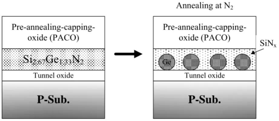
3.2. Formation and Nonvolatile memory effect of Germanium Nanocrystal embedded in Nitride layer using Silicon-Germanium-Nitride layers 3.2.1 Introduction---54
3.2.2 Experiment---55
3.2.3 Results and discussion---56
3.2.4 Conclusion---58
Chapter 4 Nickel-silicide Nanocrystals Nonvolatile Memories
4.1. Electrical Characteristics of Nonvolatile Nickel-Oxygen-Silicon (Ni-O-Si) Nanocrystals memory 4.1.1 Introduction---664.1.2 Experiment---69
4.1.3 Results and discussion---70
4.1.4 Conclusion---73
4.2. Electrical Characteristics of Nonvolatile Nickel-Silicon-Nitride (Ni-Si-N) Nanocrystals memory 4.2.1 Introduction ---80
4.2.2 Experiment---81
4.2.3 Results and discussion---82
4.2.4 Conclusion---86
4.3. Enhancement of charge storage Performance of Ni-Si-N Nanocrystals Embedded in Nitride Memory by Rapid Thermal Annealing treatment 4.3.1 Introduction---93
4.3.2 Experiment---94
4.3.3 Results and discussion---95
4.3.4 Conclusion---98
4.4. Reliability characteristics of NiSi nanocrystals embedded in oxide and nitride layer for nonvolatile memory application 4.4.1 Introduction---106
4.4.2 Experiment---107
4.4.3 Results and discussion---108
Chapter 5 Formation and Nonvolatile Memory Characteristics of
Multi-layer Nickel-silicide NCs embedded in Nitride
Layer
5.1 Introduction---118
5.2 Experiment---119
5.3 Results and discussion---120
5.4 Conclusion---123
Chapter 6 Nonvolatile Memory Effect of Single-layer and Dual
Layer Manganese Silicate (MnSiO
x) Nanocrystals
6.1 Introduction---1286.2 Experiment---129
6.3 Results and discussion---130
6.4 Conclusion---136
Chapter 7 Conclusion---
150References---
153Vita---
175Table Captions
Table 4-1 Comparisons of memory window and nanocrystal density for the Ni-O-Si and Ni-Si-N nanocrystals nonvolatile memory devices.---92 Table 4-2 Comparisons of retention for the Ni-O-Si and Ni-Si-N nanocrystals
nonvolatile memory devices.---92 Table 4-3 Comparisons of memory characteristics for Ni-Si-N nanocrystal memory before and after RTA annealing in N2.---105
Table 6-1 Comparisons of oxygen concentration for the sample C and sample D by ESCA analysis.---145
Figure Captions
Chapter 1
Figure1.1 Structure of the conventional floating-gate nonvolatile memory device. Continuous poly-Si floating gate is used as the charge storage element. Figure1.2 Tunnel oxide and operation voltage scaling predicted by the 2007
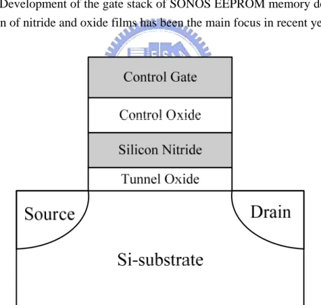
International Technology Roadmap for Semiconductors.---14 Figure1.3 Development of the gate stack of SONOS EEPROM memory devices. The optimization of nitride and oxide films has been the main focus in recent years.
Figure1.4 Structure of the SONOS nonvolatile memory device. The nitride layer is used as the charge trapping media.---15 Figure1.5 Structure of the nanocrystal nonvolatile memory device. The nanocrystals are used as the charge storage element instead of the continuous poly-Si floating gate.
Figure1.6 Energy band diagrams of (a) Ge, (b) Ni and (c) HfO2 nanocrystals
nonvolatile memories. Sub.: Silicon substrate, Box.: Blocking oxide, G: Gate.---16
Chapter 2
Figure2.1 I–V curves of an FG device when there is no charge stored in the FG (curve A) and when a negative charge is stored in the FG (curve B).---18 Figure2.2 Fourth approaches to programming methods, described by Hu and White. ---21 Figure2.3 Schematic cross section of MOSFET. The lateral electric field (E)
in electron injection. ---24 Figure2.5 Schematic sketch and energy band diagram of Band to Band Hot Electron
Tunneling Injection.
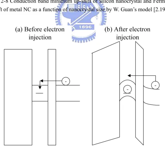
Figure2.6 Schematic sketch and energy band diagram of Band to Band Hot Hole Tunneling Injection.---26 Figure2.7 Schematic sketch and energy band diagram of Channel Initiated Secondary Electron Injection.---27 Figure2.8 Conduction band minimum up-shift of silicon nanocrystal and Fermi level up-shift of metal NC as a function of nanocrystal size by W. Guan’s model. Figure2.9 Schematic energy band diagram of coulomb blockade effect (a) before
electron injection, and (b) after one electron injection.---30 Figure2.10 Energy band diagram of a SONOS device in the excess electron state,
showing retention loss mechanisms: trap-to-band tunneling (TB), trap-to-trap tunneling (T-T), band-to-trap tunneling (B-T), thermal excitation (TE) and Poole–Frenkel emission (PF).---32 Figure2.11 Endurance requirement as a function of memory capacity.---33 Figure2.12 Threshold voltage window closure as a function of program/erase cycles
on a single cell due to the degradation of tunnel oxide.---34 Figure2.13 Anomalous stress induced leakage current (SILC) modeling. The leakage is caused by a cluster of positive charge generated in the oxide during erase.---35
Chapter 3
Figure3.1 The XPS analysis by using an Al Kα (1486.6 eV) x-ray radiation is demonstrated the chemical composition of (a) Si 2p, (b) Ge 3d and (c) O 1s core-level spectra.---46
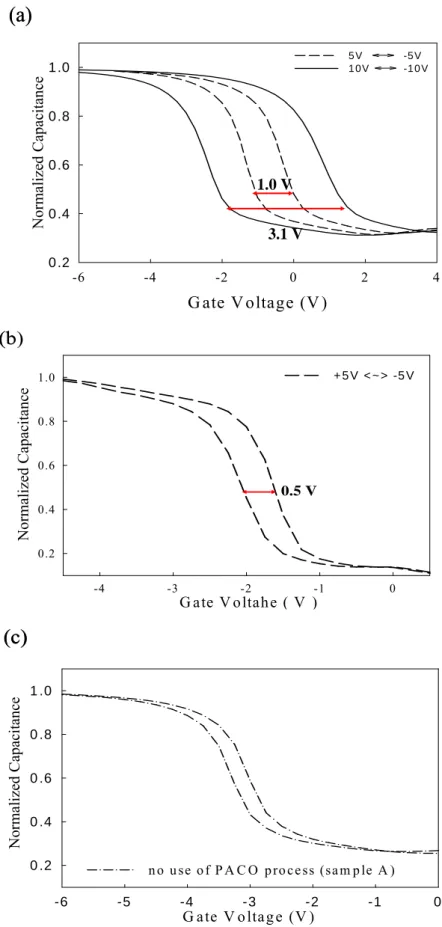
Figure3.2 Formation flow of Ge nanocrystals MOIOS structure. ---47 Figure3.3 (a) Cross-sectional transmission TEM analysis of MOIOS structure with Ge nanocrystal embedded in oxide (the nanocrystals size and density are about 5-6 nm and 1.73×1012 cm-2, respectively) and inset is the lattice image of Ge nanocrystal. (b) XPS analysis of the Ge 3d core-level spectrum. The Ge-O signal is at about 31 eV shift to lower bonding energy 29 eV which is the Ge-Ge signal peak position after RTA process.---48 Figure3.4 (a) Cross-sectional transmission TEM analysis of MOIOS structure with GeO nanocrystal embedded in oxide (the nanocrystals size and density are about 5-6 nm and 4.4×1011 cm-2, respectively). (b) XPS analysis of the Ge 2p core-level spectrum and the Ge-O signal is at about 1220 eV after RTA process.---49 Figure3.5 Electrical characteristics of C-V hysteresis under ± 5 gate voltage
operation with (a) sample A(use of PACO step), (b) sample B (use of PACO step), and (c) sample A(no use of PACO step). ---50 Figure3.6 Secondary ion mass spectrometer (SIMS) analysis of MOIOS structure
with Ge of before annealing, sample A, and no use of PACO (sample A). Figure3.7 Energy band diagrams of (a) sample A and (b) sample B. The band gap of
Ge and GeO2 are 0.6 and 3.92 eV [3.24].---51
Figure3.8 Programming and erasing characteristics of the Ge nanocrystals embedded in oxide under ± 5 V gate voltage operation.
Figure3.9 Endurance characteristics of Ge nanocrystals embedded in oxide under the pulse conditions of VG - VFB = ±5 V for 1 ms. The flat-band voltage
can be defined by using the C-V hysteresis.---52 Figure3.10 Retention time test with Ge nanocrystal embedded in oxide at room
holding ratio of is 25% after 10ys.---53 Figure3.11 Formation flow of Ge nanocrystals embedded in SiNx MOIOS
structure.---59 Figure3.12 XPS analysis by using an Al Kα (1486.6 eV) x-ray radiation is
demonstrated the chemical composition of (a) Si 2p , (b) Ge 3d and (c) N 1s core-level spectra for Si2.67Ge1.33N2 thin layer.---60
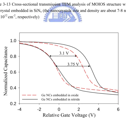
Figure3.13 Cross-sectional transmission TEM analysis of MOIOS structure with Ge nanocrystal embedded in SiNx (the nanocrystals size and density are about
7-8 nm and 1.12×1012 cm-2, respectively)
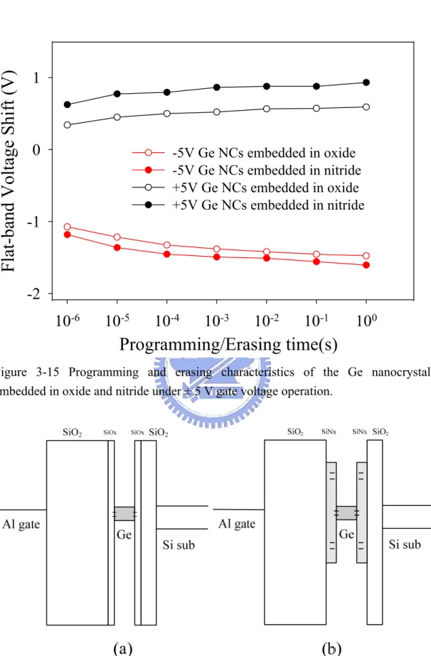
Figure3.14 Electrical characteristics of C-V hysteresis under ± 10 gate voltage operation with Ge nanocrystals embedded in oxide and nitride.---61 Figure3.15 Programming and erasing characteristics of the Ge nanocrystals embedded
in oxide and nitride under ± 5 V gate voltage operation.
Figure3.16 Energy band diagrams of Ge nanocrystals embedded in (a) oxide and (b) nitride. The band gap of Ge and SiNx are 0.6 and 5.1 eV. The trap level of
SiNx below the conduction band energy of SiNx is about 0.8 – 1.5 eV.---62
Figure3.17 Retention time test with Ge nanocrystal embedded in (a) oxideand (b) nitride at room temperature operating a ±15 V gate voltage stress for 10 s. The charge holding ratio of are 25% and 33% for the Ge nanocrystal embedded in (a) oxideand (b) nitride after 10ys, respectively.---63 Figure3.18 Current density-gate voltage (J-V) of Ge nanocrystals embedded in oxide and nitride.---64 Figure3.19 Endurance characteristics of Ge nanocrystals embedded in (a) oxide and (b)
nitride under the pulse conditions of VG - VFB = ±5 V for 1 ms. The
Chapter 4
Figure4.1 Formation flow of nanocrystals embedded in oxide MOIOS structure. Figure4.2 Formation flow of control sample MOIOS structure (Oxygen deficient
Ni0.3Si0.7 layer as charge trapping layer).---74
Figure4.3 Cross-sectional TEM analyses of (a) control sample, and (b) MOIOS structure containing nanoparticles. The nanocrystal size and density are about 5-6 nm and 1.33×1012 cm-2, respectively. The inset shows sketch diagrams of control sample and MOIOS structure.---75 Figure4.4 Capacitance-voltage (C-V) hysteresis of MOIOS structure with (a) the
control sample, and (b) NiOSi nanoparticles. The memory windows of NiOSi nanoparticles, 0.8 V and 2.5 V, can be obtained under ±10 (dash line) V and ±15 V (solid line) gate voltage operation, respectively.---76 Figure4.5 (a) Ni 2p and (b) O 1s X-ray photoelectron spectroscopy (XPS) analysis of the charge trapping layer. Empty circles and straight line indicate experimental and fitting results, respectively.---77 Figure4.6 (a) Retention characteristics of the memory structure with NiOSi
nanoparticles using a ±10 V gate voltage stress for 5 sec at room temperature. The dotted line is the extrapolated value of retention data after 100 sec. (b) Programming and erasing characteristics of the NiOSi nanoparticles under ±10 V and ±15 V gate voltage.---78 Figure4.7 Endurance characteristics of Ni-O-Si nanocrystals embedded in oxide
under the pulse conditions of VG - VFB = ± 5 V for 0.1 ms. The flat-band
voltage can be defined by using the C-V hysteresis.---79 Figure4.8 Schematic sketches of the experimental procedures. Nitrogen incorporated Ni0.3Si0.7 layer as charge trapping layer was fabricated the nanocrystal
nonvolatile memory.
Figure4.9 Cross-sectional TEM image of the MOIOS structure with nanocrystals during our proposed fabrication. The inset was a schematic sketch of MOIOS.---87 Figure4.10 (a) Ni 2p XPS analysis of the charge trapping layer. The Ni 2p3/2 peak can
be assigned to Ni-Si-N ternary bond (~ 855 eV). (b) N 1s XPS analysis of the charge trapping layer. Empty circles and straight line indicate experimental and fitting results, respectively.
Figure4.11 (b) N 1s XPS analysis of the charge trapping layer. Empty circles and straight line indicate experimental and fitting results, respectively.---88 Figure4.12 Capacitance-voltage (C-V) hysteresis of the fabricated MOIOS structure
with the Ni-Si-N nanocrystals embedded in SiNx matrix as a charge
trapping layer. The inset shows current density-voltage (J-V) characteristics.---89 Figure4.13 Retention characteristics of the memory structure with Ni-Si-N
nanocrystals embedded in SiNx matrix using a ±10 V gate voltage stress
for 5 sec at room temperature. The dotted line is the extrapolated value of retention data after 1000 sec.---90 Figure4.14 Endurance characteristics of the Ni-Si-N nanocrystal nonvolatile memory. The memory window is about 1.0 V after one million P/E cycles operation. Figure4.15 Current density-voltage (J-V) characteristics of the MOIOS nonvolatile
memory structures with the control sample, Ni-O-Si nanocrystals and Ni-Si-N nanocrystals.---91 Figure4.16 Formation flow of NiSi nanocrystals embedded in nitride layer by using rapid thermal annealing treatment in N2 ambiance.---99
nanocrystals (Empty circles and straight line indicate experimental and fitting results, respectively). (b) Leakage current density (A/cm2) with gate voltage and (c) X-ray diffraction (XRD) analysis of the nanocrystals during different thermal annealing temperature (Control sample is only a structure of Si substrate with 5-nm tunnel oxide).---100 Figure4.18 C-V hysteresis and TEM image (inset) of NiSi nanocrystals nonvolatile
memories (500oC). The memory window was 5.0 V under ± 10 V operation.
Figure4.19 C-V hysteresis and TEM image (inset) of NiSi nanocrystals nonvolatile memories (600oC). The memory window was 4.0 V under ± 10 V operation.---101 Figure4.20 Retention characteristics of the NiSi nanocrystals nonvolatile memories
through RTA treatment at (a) 500 oC for 100 sec and (b) 600 oC for 100 sec.---102 Figure4.21 Endurance characteristics of the NiSi nanocrystals nonvolatile memories
through RTA treatment at (a) 500 oC for 100 sec and (b) 600 oC for 100 sec. Figure4.22 Energy band diagrams of (a) Ni-N NCs (STD), (b) Ni-Si NCs (500oC) and (c) Ni-Si NCs (600oC) embedded in nitride layer.---105 Figure4.23 Formation flow of NiSi nanocrystals embedded in nitride and oxide
nonvolatile memories.---111 Figure4.24 Cross-sectional TEM analysis of (a) NiSi NCs embedded in oxide layer, and (b) NiSi NCs embedded in nitride layer. C-V hysteresis of memory structure with (c) NiSi NCs embedded in oxide layer and (d) NiSi NCs embedded in nitride layer. The memory windows of (c) 2.0 V and (d) 4.0 V can be obtained under ±10 gate voltage operation, respectively.---112
(charge holding rate: 50%) and (b) nitride layer (charge holding rate: 56%). The dotted line is the extrapolated value of retention data after 100 s, which this range is a steady state.---113 Figure4.26 Endurance characteristics of the NCs memory structure embedded in (a)
oxide layer and (b) nitride layer. Pulses condition of VG - VFB = ±5 V for 0.1 ms.---114 Figure4.27 Simulation of electric field distribution of NiSi NCs embedded in oxide layer. The red line/black line of inset is a distribution of vertical electric field across a single NC/without any NCs. The simulation structure conditions of tunnel oxide thickness, metal NCs diameter, blocking oxide thickness, distance between NCs and tunnel oxide or blocking oxide are set 3 nm, 5 nm, 30 nm, and 2 nm. In addition, the dielectric constants of SiO2 and SiN were given to 3.9 and 7.5, respectively.---115
Figure4.28 Simulation of electric field distribution of NiSi NCs embedded in nitride layer. The red line/black line of inset is a distribution of vertical electric field across a single NC/without any NCs. The simulation structure conditions of tunnel oxide thickness, metal NCs diameter, blocking oxide thickness, distance between NCs and tunnel oxide or blocking oxide are set 3 nm, 5 nm, 30 nm, and 2 nm. In addition, the dielectric constants of SiO2 and SiN were given to 3.9 and 7.5, respectively.---116
Figure4.29 Schematic sketches of stored charges transportation under Program/Erase operation for the MOIOS structure containing NiSi nanocrystals embedded in (a) oxide and (b) nitride.---117
Chapter 5
Figure5.1 Cross-sectional transmission electron microscope and fabrication flow of NiSi NCs embedded in the nitride layer (Single-layer NCs nonvolatile
memory).
Figure5.2 Cross-sectional transmission electron microscope and fabrication flow of NiSi NCs embedded in the nitride layer (Multi-layer NCs nonvolatile memory).---124 Figure5.3 Capacitance-voltage (C-V) hystereses of memory structure with (a)
single-layer and (b) multi-layer NCs. The memory windows of (a) 4.0 V and (b) 13.0 V can be obtained under ±10 gate voltage operation, respectively.
Figure5.4 Endurance characteristics of (a) multi-layer NiSi NC memory and (b) single-layer NiSi NC memory. Pulses condition of VG - VFB = ±5 V and
0.1 ms.---125 Figure5.5 Retention characteristics of the NCs memory structure with (a) room temperature, 27°C and (b) 85°C. The dotted line and solid line are the extrapolated value of retention data after 1000 s, which this range is a steady state.---126 Figure5.6 Energy bond diagram of multi-layer NiSi NCs embedded in SiNx. The
ground states of first and second layer of multi-layer structure were caused by the energy level quantization effect.---127
Chapter 6
Figure6.1 Schematic sketches of experimental procedures for manganese silicate nanocrystals embedded in oxide layer nonvolatile memories. Sample C is used the RTA process in O2 ambiance. Sample D is used the oxygen
incorporated Mn0.2Si0.8 layer as charge trapping layer.---138
Figure6.2 Cross-section (a) and plane view (b) TEM images of sample C. (c) Cross-section TEM image of sample D.
circles and straight line indicate experimental and fitting results, respectively.---139 Figure6.4 C-V hysteresis of MOIOS structures by (a) sample C, and (b) sample D.
The memory windows of two samples are nearly equal to 1 and 2.5 V under ±5 dash line and ±10 V solid line gate voltage operation, respectively.---140 Figure6.5 Endurance characteristics of the NCs memory structures by the (a) sample C and (b) sample D. Pulses condition of VG−VFB= ± 10V for 10 ms.----141
Figure6.6 Retention characteristics of the NCs nonvolatile memory structures by the sample C and sample D. Charge holding rates of sample C and sample D are about 35% and 52% after 10 ys.
Figure6.7 Valence band spectrum for Si-sub, 5 nm thick SiO2/Si (100) and 5 nm
thick MnSiOx/Si (100) by using the XPS analyses. The valance band offset
(△EV) of MnSiOx for our proposed sample is about 2.8 eV.---142
Figure6.8 O1s energy-loss spectra for 5 nm thick thermal oxide and 5nm thick MnSiOx by using the XPS analyses. The band gap (Eg) of manganese
silicate is about 5.8 eV.
Figure6.9 Energy band diagram of MOIOS memory cell with MnSiOx nanocrystals
as charge trapping center.---143 Figure6.10 Current–density J (A/cm2) as a function of the VOX of a MOS capacitor
with a MnSiOx stack dielectric layer (8 nm MnSiOx) recorded from 25 to
150 °C.
Figure6.11 Current–density J (A/cm2) of (a) sample C and (b) sample D as a function of the inverse temperature for MnSiOx gate dielectric stacks. The solid
lines are fitted to the data by using Eq. (10-6). The Φt of (a) sample C and
Figure6.12 (a) Trapping levels below the conduction band of MnSiOx NCs by the
sample C (blue line) and sample D (red line). Escaping paths of stored charges for the (b) sample C and (c) sample D are form the trapping level of NCs to the Si sub. under retention state.---145 Figure6.13 (a) Lateral leakage current phenomenon of non-ideal double metal NCs
structure. (b) Our proposed double layer MnSiOx NCs structure.
Figure6.14 Formation flow of our proposed double layer MnSiOx NCs structure by
using the self-assembled mechanism of MnSiOx NCs.---146
Figure6.15 Cross-section TEM image of our proposed double MnSiOx NCs
nonvolatile memory structure.
Figure6.16 C-V hystereses of MOIOS structures by the (a) double layer NCs and (b) single layer NCs. The memory windows are 4.5 and 2.5 V for the (a) double layer NCs and (b) single layer NCs under VG-VFB= ± 10 V solid
line gate voltage operation, respectively.---147 Figure6.17 Flat band voltage shift characteristics of the double layer MnSiOx
nanocrystals NVM as compared with single-layer MnSiOx nanocrystals
NVM for the electron injection. The Flat band voltage shift is measured by C-V curve.
Figure6.18 Energy band diagrams of electrons injection under (a) small gate voltage (VG-VFB≦4 V) and (b) high gate voltage (VG-VFB≧4 V) operations.---148
Figure6.19 Retention characteristics of the double layer MnSiOx nanocrystals NVM as
compared with single layer MnSiOx nanocrystals NVM. Charge holding
rates of double layer and single layer MnSiOx nanocrystals NVMs are
about 64% and 52% after 10 ys.
Chapter 1
Introduction
1.1 Overview of Nonvolatile Memory
Recently, the portable electronic products can provide the convenient life for human. These products all need the flash memories which are considered as a technology driver for next-generation semiconductor industry. It can be classified into two major markets: code storage and data storage applications. NOR type flash memory has been targeted at code storage application, such as PC bios and DVD player [1.1]. NAND type flash memory is most suitable for the code storage application [1.2], such as PDA, memory cards, MP3 audio players, digital cameras, and USB flash personal disc etc. These products all are based on flash memories that are nonvolatile and can keep stored information when the power supply is switched off. Flash memory also has exhibited several advantages, such as the ability to be electrical programmed and fast simultaneous block electrical erased in a single-cell, smallest cell size to achieve a highest chip density, and good flexibility [1.3, 1.4]. The flash memory fabrication process can be compatible with the current CMOS process and be a suitable solution for the embedded memory application. Flash memories are easily scaled down to replace for EPROMs (Erasable Programmable Read Only Memory) and EEPROMs (Electrically Erasable Programmable Read Only Memory). As these critical advantages flash memory possesses, it has become the mainstream nonvolatile memory device in last few decades.
In 1967, D. Kahng and S. M. Sze invented the floating-gate (FG) nonvolatile semiconductor memory (or flash memory) at Bell Labs [1.5]. A standard conventional FG device structure is shown in Fig. 1-1. The structure is basic on a Metal Oxide
Semiconductor Field Effect Transistor (MOSFET) with a modified stacking gate which composed by control gate, dielectric, floating gate and dielectric as a sandwich structure. Charges injected in the FG are maintained there, allowing the difference between threshold voltages of the cell transistor for nonvolatile memory (NVM) application.
Nowadays, NVM devices are moving toward high density memory array, low cost, low power consumption, high-speed operation, and good reliability. However, the conventional FG NVMs have their limitation which the most prominent one is the limited potential for the continued scaling of device structure. This scaling limitation stems from the extreme requirements of tunnel oxide layer. The tunnel oxide must be thin enough to allow the charges to transfer fast to the FG. According to the 2007 International Technology Roadmap (ITRS) of Semiconductor flash memory [1.6], the FG memory devices have to reduce the tunnel oxide thickness to 6-7 nm in 2010s, as shown in Fig. 1-2. Moreover, the scaling of the gate stack and operation voltages is often related to each other. A tunnel oxide thickness of more than 8 nm is currently used in the commercial flash memory chip to meet the ten years data retention time requirement. If the tunnel oxide were to be scaled below 2 nm, the operation voltage could be reduced from more than 10 V to below 4 V [1.7]. Unfortunately, the retention time would also be reduced, from 10 years to several seconds. The tunnel oxide needs to provide superior isolation under retention, endurance, and disturbed conditions in order to guarantee the data integrity for 10 years. Hence, for faster operation speed, thin tunnel oxide is desirable. Nevertheless, it is also desirable to increase the thickness of tunnel oxide for the better isolation and reliability. There is a trade-off between speed and reliability for the optimum tunnel oxide thickness [1.8].
induce a leakage path that will make all charges stored in the FG leak back to the channel. To alleviate the trade-off of tunnel oxide design for FG memory devices, memory-cell structures employing discrete traps as charge storage media have been proposed in the past few years. Unlike conventional continuous FG, charges stored in the discrete nodes cannot easily redistribute amongst themselves. Therefore, only a relatively small number of nodes near the oxide defects will be affected. Local charge storages in the discrete nodes can enables more aggressive scaling of tunnel oxide by relieving the total charge loss concern. Therefore, two suggestions, poly-Si/oxide/nitride/oxide/Si (SONOS) [1.7-1.9] and nanocrystal nonvolatile memory devices [1.10-1.12] are proposed to overcome this oxide quality limit of the conventional FG structure. Hence the tunnel oxide thickness can be reduced to allow faster programming and lower voltage operation.
1.1.1 SONOS Nonvolatile Memory Devices
The first nitride-base devices is metal-gate nitride device MNOS (Metal/Nitride/Oxide/Silicon) which was reported in 1967s by Wegener et al. [1.13]. However, it is well known that silicon nitride film contains much carrier traps which cause a threshold voltage shift. Then the silicon nitride trap-based devices are widely studied for charge storage device application in the early 1970s. Fig. 1-3 illustrates the progression of device cross section, which has led to the present SONOS device structure. Initial device structures in the early 1970s were p-channel metal-nitride-oxide-silicon (MNOS) structures with aluminum gate electrodes and thick (45nm) silicon nitride charge storage layers. Write/erase voltages were typically about 25-30 V. In the late 1970s and early 1980s, the NVM devices moved to n-channel SNOS devices with write/erase voltages of 14-18 V. In the late 1980s and early 1990s, n- and p-channel SONOS devices emerged with write/erase voltages of
5-12 V. The ONO triple dielectric structure has some advantages, such as (1) lower programming voltage since the blocking action of the top oxide removes any limitation on the reduction of the nitride thickness; (2) charge injection from and to the gate electrode is minimized for both gate polarities, particularly for hole injection; (3)improved memory retention since there is a minimal loss of charge for the gate electrode.
The SONOS (poly-Silicon-Oxide-Nitride-Oxide-Silicon) memory devices, as shown in Fig. 1-4, have attracted a lot of attention due to its advantages over the traditional FG flash device. These include reduced process complexity, lower voltage operation, high speed operation, improved cycling endurance, and elimination of drain-induced turn-on [1.14-1.15]. The main difference between FG and SONOS structure is the method of charge storage. Conventional FG structure charges carriers in the continuous conductive polysilicon. In contrast with conventional FG structure, SONOS structure charges carriers in the physical discrete traps of the silicon nitride dielectric. Typical traps have a density of the order 1018-1019 cm-3 according to the calculation of Yang et al. [1.16] and can store both electrons and holes injected from the channel. The charges stored in the silicon nitride cannot move easily, hence the SONOS can tolerate the defects in the tunnel oxide induced the leakage path. Therefore, the SONOS memory device has better endurance than the conventional FG memory.
The SONOS memory devices still face challenge in the future for high density NVM application, which requires low voltage (< 5V), low power consumption, long-term retention, and superior endurance. Various approaches have been proposed for improving the SONOS performance and reliability. Chen et al. demonstrate a Si3N4 bandgap engineering (BE) control method for better endurance and retention. A
charge-trapping efficiency significantly [1.17].
In recent research, high-k dielectric materials were proposed to replace the silicon nitride film as the charge trapping layer, such as HfAlO and Al2O3. Tan et al.
showed that over-erase phenomenon in SONOS memory structures can be minimized by replacing silicon nitride with HfO2 as the charge storage layer. The charge
retention and endurance performance is improved by the addition of 10% Al2O3 in
HfO2 to form HfAlO thin film served as charge trapping layer, while maintaining the
over-erase resistance of HfO2 [1.18]. She et al. demonstrates that high-quality nitride
is applied as the tunnel dielectric for a SONOS-type memory device. To compare control devices with SiO2 tunnel dielectric, faster programming speed and better
retention time are achieved under a low programming voltage [1.19]. Lee et al. present a device structure of SiO2/SiN/Al2O3 (SANOS) with the TaN metal gate. It is
demonstrated that the use of TaN metal gate can block electron current through Al2O3
layer more efficiently than a conventional polysilicon gate, resulting in faster program/erase speed and significant decrease of the saturation level of the erase VT
[1.20].
Chen et al. studies a polycrystalline silicon thin-film transistor (poly-Si TFT) with oxide/nitride/oxide (ONO) stack gate dielectrics and multiple nano-wire (NW) channels for the applications of both nonvolatile SONOS memory and switch transistor [1.21]. The proposed NW SONOS-TFT exhibits superior memory device characteristics with high program/erase efficiency and stable retention characteristics at high temperature. Such SONOS-TFT is thereby highly promising to apply for the future system-on-panel (SOP) display applications.
New device structures are also indispensable in making flash memory more scalable. Since SONOS flash memory offers a thinner gate stack than floating gate flash memory, and a FinFET structure controls the short channel effect much better
than a bulk structure. It has been demonstrated that the FinFET SONOS flash memory devices with a much smaller cell size can provide both excellent performance and reliability. Therefore, FinFET SONOS memories have also potential to become the candidates of the next generation flash memories [1.22-1.13].
1.1.2 Nanocrystal Nonvolatile Memory Devices
Nanocrystal nonvolatile memories are one particular implementation of storing charge by dielectric surrounding with nanocrystals, and were first introduced in the early 1990s by IBM researchers who proposed flash memory with a granular floating gate made from silicon nanocrystals [1.24]. The name nanocrystal referred to a crystalline structure with a nanoscale dimension. Fig. 1-5 illustrates a typical nanocrystal NVM device structure and it is observed that the nanocrystals are separated from each other within the gate dielectric. Its electronic properties seem more similar to an atom or molecule rather than the bulk crystal. In the nanocrystal NVM device, the charges were charged in the isolated nanocrystals instead of the continuous FG polysilicon layer. Each nanocrystal will typically store only a handful of electrons and the charges stored in these dots collectively control the channel conductivity of the memory transistor.
Nanocrystal-based NVM devices have recently received much attention due to their potential to overcome the limitations of conventional FG flash memory for the scaling down tunnel oxide process. Using nanocrystals as charge storage media offers several advantages, the main one being the potential to use thinner tunnel oxide (< 5 nm) without sacrificing non-volatility. This is a quite attractive proposition since reducing the tunnel oxide thickness is a key to reduce the operating voltage and speed. This claim of improved scalability results from the local charge storage in discrete
by localized oxide defects. Further, the lateral charge migration effect between nanocrystals can be suppressed by the strongly isolation of surrounded dielectric. There are other important advantages except the above-mentioned benefits. First, nanocrystal memories use a more simplified fabrication process as compared to conventional stacked-gate FG NVMs by avoiding the fabrication complications and costs of a dual-poly process. Second, due to the absence of drain with FG coupling, nanocrystal memories suffer less from drain-induced-barrier-lowering (DIBL). One way to exploit this advantage is to use a higher drain bias during the read operation and to improve memory access time [1.25]. Hence, nanocrystals NVMs are allowed the use of shorter channel lengths to achieve the high density cell. Finally, nanocrystal memories are characterized by excellent immunity to stress induced leakage current (SILC) and oxide defects due to the distributed nature of the charge storage in the charge trapping layer. Research in this regime has focused on the development of fabrication processes, nanocrystal materials and the integration of nanocrystal-based storage layers in actual memory devices.
A nanocrystal NVM fabrication requires a perfect control of four main parameters: (1) the tunnel oxide thickness, (2) the nanocrystal density, (3) the nanocrystal size, and (4) the control oxide thickness. An important consideration is the average size and distributable density of nanocrystals. Larger-size nanocrystal array provides higher programming/erasing (P/E) efficient due to small quantum confinement and coulomb blockade effects. However, it is desirable to reduce the nanocrystal size leading to the high density on the channel for a uniform devices array. Therefore, there is a trade-off in selecting the nanocrystal size. A typical target is a density of at least 1011-1012 cm-2, and requires nanocrystal size of 5-10 nm. Moreover, good process control is needed with regards to such nanocrystal features as: planar nanocrystal layer; inter-nanocrystal interaction (lateral isolation); and nanocrystal
shape. We prefer that the fabrication processes are simple and compatible with the standard semiconductor equipment.
Currently, the nanocrystals NVMs can be classified three major categories by the materials: (1) semiconducting, (2) metallic and (3) high-k dielectric nanocrystals. Figure 1-6 shows the energy band diagrams of (a) Ge, (b) Ni and (c) HfO2
nanocrystals nonvolatile memories. In this thesis, the authors will intro the developments and advantages of three kinds of nanocrystals.
A. Semiconducting Nanocrystal Memories
After the first proposal of a memory transistor using silicon nanocrystals as floating gates. In order to improve the data retention in NVM, double layer Si nanocrystals memory has been investigated [1.26]. It seems interesting to use Ge nanocrystals rather than Si nanocrystals because of its smaller band gap (~ 0.6 eV), as shown in Fig. 1-6(a). Indeed King and Hu et al. have recently demonstrated the superior memory properties of Ge based nanocrystal memories over those based on Si [1.27]. Recently, germanium/silicon (Ge/Si) heterojunction nanocrystals have been reported to possess superior charge retention capability than single Ge or Si nanocrystals. This is due to the fact that Ge has a smaller band gap than Si, and thus by introducing a Si interface around the Ge nanocrystal, it can create an additional barrier height between the Ge and Si interface to prevent the stored charges to leak out of the nanocrystals [1.28, 1.29]. However, semiconductor nanocrystal memory may not be the ultimate solution to nonvolatile memory scaling, although it still attracts a lot of attention now.
B. Metallic Nanocrystal Memories
In optimizing nanocrystal NVM devices, the ideal goal is to achieve the fast write/erase of DRAM and the long retention time of Flash memories simultaneously.
dielectric to maximize the IG, Write/Erase/ IG, Retention ratio. One approach for achieving
this goal is to engineer the depth of the potential well at the storage nodes, thus creating a large energy band offset between the Si substrate and the storage nodes for programming speed and retention operation. This can be achieved if the storage nodes are made of metal nanocrystals by engineering the metal work function. The major advantages of metal nanocrystals over semiconductor nanocrystals include (1) higher density of states around the Fermi level, (2) scalability for the nanocrystal size, (3) a wide range of available work functions, and (4) smaller energy perturbation due to carrier confinement [1.30]. In addition, an electrostatic modeling from both analytical formulation and numerical simulation is demonstrated that the metal nanocrystals will significantly enhance the electric field between the nanocrystal and the sensing channel set up by the control gate bias, and hence can achieve much higher efficiency in low-voltage P/E [1.31].
Toward better NVM device performance and reliability, numerous attempts have been made using metal nanocrystals. Liu et al. reported the growth of Au, Pt, and Ag nanocrystals on SiO2 using an e-beam deposition method [1.32]. Lee et al. proposed a
NVM structure using the Ni nanocrystals and high-k dielectrics [1.33]. Chen et al. present the stacked Ni silicide nanocrystal memory was fabricated by sputtering a commixed target followed by a low temperature RTO process [1.34]. W nanocrystals on atomic-layer-deposited HfAlO/Al2O3 tunnel oxide were presented for application
in a memory device [1.35]. Using W nanocrystal double layers embedded in HfAlO to enhancement of memory window was demonstrated from the short channel devices down to 100nm [1.36]. Tang et al. demonstrate that a chaperon in protein lattice can be used as a template to assemble PbSe and Co nanocrystal arrays for Flash memory fabrication. This provides a new approach to achieve a high density and good distribution uniformity nanocrystal array [1.38].
C. High-K dielectric Nanocrystal Memories
The high-k dielectric nanocrystal nonvolatile memories (HfO2 and CeO2
nanocrystals) are first proposed by C. H. Chien et al. [1.39, 1.40]. C. H. Chien et al. reported a method of co-sputtering Hf and Si in oxygen followed with high-temperature annealing to form the high-K dielectric nanocrystals for SONOS-type memory devices. These devices are not only like SONOS-type nonvolatile memories but also can restrain the stored charge lateral migration effect. Hence, the performance of high-k dielectric nanocrystals for 2-bits operation is better than SONOS-type memory devices.
In the future, the primary drivers behind nanocrystal memories are the potential to scale the tunnel oxide thickness, resulting in lower operating voltages, and the simplicity of a single poly-silicon process. But there are still challenges await nanocrystal memories in the long road to commercialization. Nanocrystal memories have yet to deliver on most of their promises. In reality, part of the voltage gain is offset because of the poor control gate coupling. For fabrication processes, it is hard to control the uniformity of the nanocrystal size and their physical locations in the channel. It is not a surprise that nanocrystal memories exhibit large device-to-device variation. Moreover, it has yet to be demonstrated that both the nominal and the statistical retention behavior are sufficient to meet true non-volatility requirements. Although single-dot memories have been demonstrated [1.41,1.42], but a more fundamental understanding of the scaling limits of nanocrystal memories is necessary, concentrating especially on the aspect of controlling channel conductance when relying on only a few discrete charge centers [1.43, 1-44]. Finally, in order for that to happen, their claimed benefits will need to be more unambiguously substantiated, and a more appealing bundle of memory features will have to be demonstrated.
1.2
Motivation
The Semiconductor Industry Association (SIA) International Technology Roadmap for Semiconductors (ITRS) indicates the difficult challenge, beyond the year 2007, for nonvolatile semiconductor memories is to achieve reliable, low-power, low-voltage performance [1.6]. For nonvolatile flash memories, two limitations encountered at the present time are: (1) the limited potential for continued scaling of the device structure. This scaling limitation stems from the extreme requirements put on the tunnel oxide layer. In order to get balance between program/erase speed and retention time, there is a trade-off between speed and reliability to get the optimal tunnel oxide thickness; (2) the quality and strength of tunnel oxide (or tunnel dielectric) after plenty of program/erase cycles. Once a leaky path has been created in tunnel oxide, all the charges stored in the floating gate will be lost. Therefore, two suggestions, the SONOS and the nanocrystal nonvolatile memory devices, are proposed to overcome this oxide quality limit of the conventional FG structure. These technologies replace the floating gate structure with a great number of charge-storage nodes in the dielectric or in the nanocrystal. Unlike the floating gate, the local leaky path will not cause the fatal loss of information for the nanocrystal nonvolatile memory device.
In this thesis, we propose three kinds of NCs with different properties (Ge, NiSi and MnSiO NCs) to overcome the limitation of conventional NVMs during the scaling down process. The proposed NCs combined with nitride layer can be efficiently improved the charge trapping ability and reliability. When a memory device has a larger memory window, it is easier to meet the requirement of retention of 10 years. And, hope to solve the two limitations mentioned above.
1.3
Organization of This Thesis
In this thesis, we propose three kinds of NCs with different properties (Ge, NiSi and MnSiO NCs) to overcome the limitation of conventional NVMs during the scaling down process.
In chapter 3, we proposed a SiGeO stacking structure serving as Ge nanocrystals self-assembled layer for application of NCs NVM. In additional we fond out that pre-annealing-capping oxide (PACO) is a critical step in our experimental process, and then we used the different oxidized competition mechanism between Si and Ge to form Ge NCs embedded in oxide. The uniform and high density (~1012cm-2) of Ge nanocrystals was fabricated after a rapid thermal annealing (RTA) process. Our propose technique compared with traditional Ge NCs process can be efficiently to prevent the over-oxidation phenomenon of Ge NC which reduces the charge trapping ability.
In chapter 4, we used the similar method that oxygen was replaced by nitrogen to form the Ge NCs embedded in SiNx structure. The memory window for the stacked
structure with Ge NCs embedded in SiNx layer is larger than Ge NCs embedded in
SiOx layer, due to the extra charge trapping centers generated from the surrounding
dielectric of Ge NCs. Furthermore, to compare these Ge NCs structures, we found that the Ge NCs embedded in nitride had better charge storage ability and reliability for NVM characteristics.
In chapter 5 and 6, an ease and low temperature fabrication technique of Ni-O-Si and Ni-Si-N NCs was demonstrated for the application of nonvolatile memory in this thesis. This result can be considered that the oxygen plays a critical role during sputter process for the formation of nanocrystal. In addition, the high
also found that high density Ni-Si-N NCs embedded in the silicon nitride (SiNx) and
larger memory effect. Therefore, by using an internal competition mechanism of charge trapping layer for these elements, we can form a metallic NCs NVM with low temperature process.
In chapter 7, 8 and 9, a RTA with temperature about 500°C and 600°C at short duration was further used to improve the crystalline quality of NCs and memory reliability. Thermal treatment can efficiently reduce the defects (leakage path) in the SiNx which surrounds the nanocrystal. The charge storage layer of NCs embedded in
SiNx shows larger memory window and better reliability over NCs embedded in SiOx,
due to different distributions of electronic field in the NC and surrounding dielectric by the simulation results. In addition, multi-layer NiSi NCs NVM structure had better charge storage and retention over than single-layer metal nanocrystals under high temperature test, due to the first and second layer of multi-layer with Quantum confinement effect depended by the NC size.
In chapter 10, for dielectric NCs process, we also used the sputter system to fabricate the manganese silicate (MnSiOx) NCs. The XPS results of charge trapping
layer can be identified the chemical state of NCs and built the energy band diagram of our produced MnSiOx thin film. Moreover, by the relationship of current density with
temperature, the trap assisted tunneling model can be used to extract the trapping level and density of MnSiOx. The oxygen doping concentration will affect the trap level
position and also influence the retention characteristics for the reliability test. Double layer MnSiOx NCs NVM also was fabricated and discussed its NVM effect. The
double layer was better trapping and keeping charges ability than single layer because the trapped charges must overcome the trap barrier and then escape from NCs due to the trapping mode of dielectric NCs.
Substrate
Tunnel oxideFloating Gate
Blocking Oxide
Control Gate
Source
Drain
Figure 1-1 Structure of the conventional floating-gate nonvolatile memory device. Continuous poly-Si floating gate is used as the charge storage element.
Figure 1-2 Tunnel oxide and operation voltage scaling predicted by the 2007 International Technology Roadmap for Semiconductors.
Figure 1-3 Development of the gate stack of SONOS EEPROM memory devices. The optimization of nitride and oxide films has been the main focus in recent years.
Figure 1-4 Structure of the SONOS nonvolatile memory device. The nitride layer is used as the charge trapping media.
Figure 1-5 Structure of the nanocrystal nonvolatile memory device. The nanocrystals are used as the charge storage element instead of the continuous poly-Si floating gate.
Figure 1-6 Energy band diagrams of (a) Ge, (b) Ni and (c) HfO2 nanocrystals
Chapter 2
Basic Principles of Nonvolatile Memory
2.1 Programming/Erasing mechanisms of nonvolatile memory
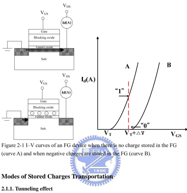
Most novel nonvolatile memories (NVMs), such as nanocrystals and SONOS memories are based on the concept of Flash memory. If a datum has to be stored in a bit of the memory, there are different procedures. The threshold voltage shift of a Flash transistor can be written as [2.1-2.3]:
FC T C Q V =− Δ (2-1)
where Q is the total charge stored in the floating gate, and CFG is the capacitances
between the floating-gate (FG) and control gate. The threshold voltage of memory cell can be altered by charging (discharging) the amount of charge into the FG and defined to the two states of the memory cell, i.e., the binary values (“1” and “0”) of the stored bit. Figure 2-1 shows the threshold voltage shift between two states in a Flash memory. The cure A of Fig. 2-1 is an initial state “1” before the programming operation and the cure B is a writing state “0” when negative charges are stored in the FG. There are many solutions to achieve “programming” or “erasing” operation. In general, tunneling effects included with direct tunneling, Fowler-Nordheim tunneling and band to band tunneling and hot carriers injections are the two kinds of operation mechanisms employed in the NVMs. These modes of stored charges transportation mechanisms will lead to difference characteristics for NVMs and the authors will briefly intro them, as follows,
Figure 2-1 I–V curves of an FG device when there is no charge stored in the FG (curve A) and when negative charges are stored in the FG (curve B).
Modes of Stored Charges Transportation
2.1.1. Tunneling effect
Tunneling mechanisms are demonstrated in the quantum mechanics. Basically, carriers tunneling injection must to have available states to exist on the other side of the barrier. If we assume elastic tunneling, this is a reasonable assumption due to the thin oxide thickness involved. In other words, there is no any energy loss during tunneling processes. The tunneling probability is depended on electron barrier height (φ(x)), tunnel dielectric thickness (d ) and effective mass (me), that is express as:
) ) ( 2 exp( 0
∫
− = d e dx m x T η ϕ (2-2)applied gate electric field. Hence, Direct tunneling (DT), Fowler-Nordheim tunneling (FN), modified Fowler-Nordheim tunneling (MFN) and trap assistant tunneling (TAT) are the main programming mechanisms employed in the NVM application. Fig. 2-2 shows these four tunnel effects approaches to programming methods.
A. Direct Tunneling effect (DT)
For nanocrystal memories, the control-gate coupling ratio of nanocrystal memory devices is inherently small [2.4]. As a result, FN tunneling cannot serve as an efficient write/erase mechanism when a relatively thick tunnel oxide is used, because the strong electric field cannot be confined in one oxide layer. When the thickness of tunnel oxide is below 5 nm, the direct tunneling is employed in nanocrystal memories instead. In the other hand, the direct tunneling is more sensitive to the barrier width than barrier height which two to four orders of magnitude reduction in leakage current can still be achieved if the metals with large work function, such as Au or Pt [2.5]. B. Fowler–Nordheim Tunneling effect (FN)
The Fowler–Nordheim (FN) tunneling mechanism occurs when applying a strong electric field (in the range of 8–10 MV/cm) across a thin oxide. In these conditions, the energy band diagram of the oxide region is very steep. Therefore, there is a high probability of electrons’ passing through the energy barrier itself. Using a free-electron gas model for the metal and the WKB approximation for the tunneling probability [2.6], one obtains the following expression for current density [2.7]:
⎥ ⎦ ⎤ ⎢ ⎣ ⎡− Φ Φ = qF m h F q J OX B B 3η ) 2 ( 4 exp 16 5 . 1 5 . 0 * 2 2 2 3 π (2-3)
where ΦB is the barrier height, m*OXis the effective mass of the electron in the
forbidden gap of the dielectric, h is the Planck’s constant, q is the electronic charge, and F is the electric field through the oxide. However, the exponential dependence of
tunnel current on the oxide-electric field causes some critical problems of process control because, for example, a very small variation of oxide thickness among the cells in a memory array produces a great difference in programming or erasing currents, thus spreading the threshold voltage distribution in both logical states.
C. Modified Fowler-Nordheim tunneling (MFN)
Modified Fowler–Nordheim tunneling (MFN) is similar to the traditional FN tunneling mechanism, yet the carriers enter the nitride at a distance further from the tunnel oxide-nitride interface. MFN mechanism is frequently observed in SONOS-type memories. The SONOS-type memory is designed for low-voltage operation (<10V, depending on the Equivalent oxide thickness), a relatively weak electric field cannot enhance charges to inject into the charging trapping layer by DT or FN mechanism.
D. Trap assistant tunneling effect (TAT)
The charge storage mediums with many traps may cause another tunneling mechanism. For example, the charges tunnel through a thin oxide and arrive to the traps of nitride layer at very low electric field in SONOS systems. During trap assisted injection the traps are emptied with a smaller time constant then they are filled. The charge carriers are thus injected at the same distance into the nitride as for MFN injection. Because of the sufficient injection current, trap assistant tunneling may influence in retention [2.8].
DT occur when OT OT OT X E X 2 1 1 > > Φ −Φ Φ FN occur when OT OT X E > Φ1
MFN occur when TAT occur when
N N ox OT OT OT X X E X ⎟ ⎠ ⎞ ⎜ ⎝ ⎛ + Φ − Φ > > Φ − Φ ε ε 2 1 2 1 N N ox OT OT OT X X E X ⎟ ⎠ ⎞ ⎜ ⎝ ⎛ + Φ > > Φ ε ε 3 3 Φ3 =Φ1−Φ2−Φt
Figure 2-2 Four tunnel effects approaches to programming methods described by Hu and White et al.
Φ1 Si Si3N4 Φ2 XOT Φ2 Φ1 Si Si3N4 XOT Φt Φ1 Si Si3N4 Φ2 XOT Φ1 Si Si3N4 Φ2 XOT
2.1.2. Channel Hot-Electron Injection (CHEI)
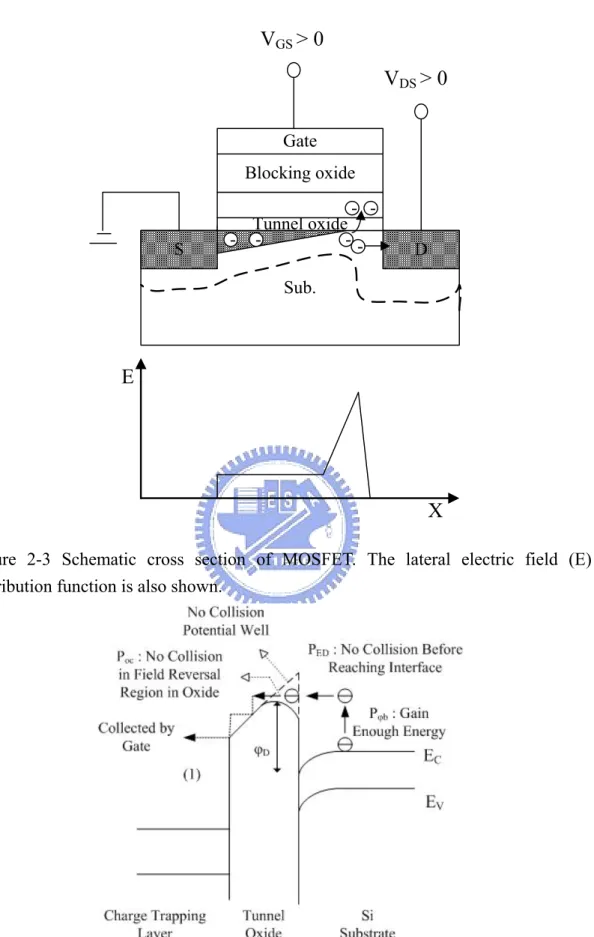
The physical mechanism of CHEI is relatively simple to understand qualitatively. An electron traveling from the source to the drain gains energy from the lateral electric field and loses energy to the lattice vibrations (acoustic and optical phonons). At low fields, this is a dynamic equilibrium condition, which holds until the field strength reaches approximately 100kV/cm [2.9]. For fields exceeding this value, electrons are no longer in equilibrium with the lattice, and their energy relative to the conduction band edge begins to increase. Electrons are “heated” by the high lateral electric field, and a small fraction of them have enough energy to surmount the barrier between oxide and silicon conduction band edges. Figure 2-3 shows schematic representation of CHEI MOSFET and the energy-distribution function with different fields. In the other hand, the effective mass of hole is heavier than one of electron. It is too hard to obtain enough energy to surmount oxide barrier. Therefore, hot-hole injection rarely is employed in nonvolatile memory operation. For an electron to overcome this potential barrier, three conditions must hold [2.10].
1) Its kinetic energy has to be higher than the potential barrier. 2) It must be directed toward the barrier.
3) The field in the oxide should be collecting it.
Nevertheless, a description of the injection conditions can be accomplished with two different approaches. The CHEI current is often explained and simulated following the “lucky electron” model [2.11]. This model is based on the probability of an electron’s being lucky enough to travel ballistically in the field G for a distance several times the mean free path without scattering, eventually acquiring enough energy to cross the potential barrier if a collision pushes it toward the Si/SiO2