應用於超寬頻3.1-10.6GHz無線接收端之疊接回授架構與低功率電流再使用架構之低雜訊放大器之設計
64
0
0
全文
(2) 應用於超寬頻3.1-10.6GHz無線接收端之疊接回授架 構與低功率電流再使用架構之低雜訊放大器之設計 Design of a cascode feedback and a low power currentreused LNA for Ultra-wideband 3.1 to 10.6GHz Wireless Receivers 研 究 生:張國慶 指導教授:荊鳳德. Student: Kuo-Ching Chang 博士. Advisor: Dr. Albert Chin. 國立交通大學 電子工程學系. 電子研究所碩士班. 碩士論文 A Thesis Submitted to Department of Electronics Engineering & Institute of Electronics College of Electrical and Computer Engineering National Chiao Tung University in Partial Fulfillment of the Requirements for the Degree of Master in Electronics Engineering. June 2006 HsinChu, Taiwan, Republic of China 中華民國九十五年六月.
(3) 應用於超寬頻3.1-10.6GHz無線接收端之 疊接回授架構與低功率電流再使用架構之 低雜訊放大器之設計 學生: 張國慶. 指導教授: 荊鳳德 博士 國立交通大學. 電子工程學系電子研究所. 摘要 本論文研製一個應用於超寬頻 3.1-10.6 GHZ 的低雜訊放大器是採用電 阻-電容疊接回授架構分別為回授 1 與回授 2,以及低功率高增益的電流再使用 架構。本研究是以 0.18 微米互補式金氧半製程實現。在回授 1 架構中,所量測 到的平均順向增益為 5dB,逆向隔離為-32dB 以下,S11 為-7.5dB 以下,S22 約 為-10dB 以下,而平均雜訊指數約為 8dB。在回授 2 架構中,所量測到的平均順 向增益為 9dB,逆向隔離為-45dB 以下,S11 為-7.2dB 以下,S22 約為-8.2dB 以 下,而平均雜訊指數約為 5.5dB。回授 1 與回授 2 架構均消耗功率 18mW。在電流 再使用架構中,所量測到的平均順向增益為 9dB,逆向隔離為-50dB 以下,S11 為-8.6dB 以下,S22 約為-8dB 以下,而平均雜訊指數約為 5.2dB。此電路消耗功 率僅為 9.4mW。. I.
(4) Design of a cascode feedback and a low power current-reused LNA for Ultrawideband 3.1 to 10.6GHz Wireless Receivers Student: Kuo-Ching Chang. Advisor: Dr. Albert Chin. Department of Electronics Engineering & Institute of Electronics Nation Chiao Tung University. Abstract A 3.1-10.6GHz low noise amplifier is applied for ultra-wideband, it introduces by the cascode R-C feedback in feedback1 and feedback2 structure and a low power, high gain current-reused structure. This research is fabricated in 0.18-μm CMOS process. In feedback1 structure, the average forward S21 is 5dB, the reverse isolation S12 is under -32dB, the S11 is under -7.5dB, the S22 is under -10dB, and the noise figure is 8dB. In feedback2 structure, the average forward S21 is 9dB, the reverse isolation S12 is under -45dB, the S11 is under -7.2dB, the S22 is under -8.2dB, and the noise figure is 5.5dB. They all consume 18mW. In current-reused structure, the average forward S21 is 9dB, the reverse isolation S12 is under -50dB, the S11 is under -8.6dB, the S22 is under -8dB, and the noise figure is 5.2dB. The circuit power consumption is only 9.4mW.. II.
(5) 誌謝 本論文得以完成,首先要感謝我的指導老師 荊鳳德 教 授,在兩年的碩士研究生涯裡,給予我豐富的指導與照顧, 不論是研究上與生活裡都讓我在這兩年裡獲得許多的收穫。 我還要感謝李秋峰學長、賴照民學長、林櫸壇學長與鄭 存甫學長他們在研究上與學業上給我的幫助,讓我得以順利 完成碩士研究。也要感謝鴻瑋、科閩、子倫以及實驗室大家, 因為有你們的陪伴與支持,讓我度過愉快又充實的兩年。 最後,我要對我的父母獻上最高的敬意與謝意,感謝父 母對我的栽培、支持與鼓勵,以及家人的陪伴,才讓我有機 會能接觸這一切並且完成我的學業與研究。. III.
(6) Contents Abstract (in Chinese)…………………………………………………………I Abstract (in English)………………………………………………………...II 誌謝…………...……………………………………………………………………III Contents………………………………………………………………………….IV Figure Captions……………………………………………………………….VI Chapter 1 Introduction 1.1 Motivation………………………………………………………………………1. Chapter 2 Noise and Nonlinear effect in RF Design 2.1 Noise………………………………………………………..……………………3 2.2 Nonlinear effect………………………………………………………………...9 2.3 Cascaded Nonlinear Stages………………………………………………....11. Chapter 3 Design of UWB LNA with cascode feedback structure 3.1 Circuit topology………………………………………………………………13 3.2 Design procedures 3.2.1 Transistor sizing and bias condition………………………………………16 3.2.2 Noise analysis……………………………………………………………..18 3.2.3 Input and output match…………………………………………………....23. IV.
(7) 3.2.4 Shunt peaking……………………………………………………………..25. 3.3 Simulation and Measurement Result………………………………….…..27. Chapter 4 Design of a low power UWB LNA with currentreused structure 4.1 Circuit topology………………………………………………………….…...36 4.2 Design procedures 4.2.1 Transistor sizing and bias condition………………………………………38 4.2.2 Input and output match…………………………………………………....40 4.2.3 Gain analysis………………………………………………….…………..42 4.2.4 Shunt peaking……………………………………………………………..44. 4.3 Simulation and Measurement Result………………………………….…..45. Chapter 5 Summary………………………………………………………...50 References……………………………………………………………………….51 Vita…………………………………………………………………………………54. V.
(8) Figure Captions Chapter 1 Introduction. Chapter 2 Noise and Nonlinear effect in RF Design Figure 2-1 Determination of input-referred noise voltage. Figure 2-2 Representation of noise in a two-port network by equivalent input voltage and current sources. Figure 2-3 (a) Definition of the 1-dB compression point, (b) Corruption of a signal due to intermodulation, (c) The third-order intercept point. Figure 2-4 Cascaded nonlinear stages.. Chapter 3 Design of UWB LNA with cascode feedback structure Figure 3-1 Proposed UWB LNA schematic (a) feedback1, (b) feedback2. Figure 3-2 (a) Simulation circuit of MOS NFmin, (b) Vgs v.s. NFmin at 3.1GHz、 6.85GHz and 10.6GHz. Figure 3-3 Noise model for the amplifying transistor M1 (a) M1 noise sources, (b) Input-referred equivalent noise generators. Figure 3-4 Equivalent circuit of the input stage for noise calculation (a) feedback1, (b). VI.
(9) feedback2. Figure 3-5 Noise figure: feedback1 v.s. feedback2. Figure 3-6 (a) Feedback1 configuration, (b) Feedback2 configuration. Figure 3-7 (a) Model of shunt-peaked amplifier, (b)Gain compare with shunt-peaking. Figure 3-8 S-parameters of feedback1 and feedback2 (a) S21, (b) S12, (c) S11, (d) S22. Figure 3-9 Noise figure of feedback1 and feedback2. Figure 3-10 Linearity of feedback1 and feedback2. Figure 3-11 Die photo (a) feedback1, (b) feedback2.. Chapter 4 Design of a low power UWB LNA with currentreused structure Figure 4-1 Proposed UWB LNA schematic. Figure 4-2 (a) Simulation circuit of MOS NFmin, (b) Vgs v.s. NFmin at 3.1GHz、 6.85GHz and 10.6GHz. Figure 4-3 Small signal model of the input impedance. Figure 4-4 Output matching network. Figure 4-5 (a) Current-reused two stage cascade amplifier with series inter-stage resonance, (b) Small signal equivalent representation of the circuit from node X to Y. Figure 4-6 1st-stage and 2nd-stage resonance contribute to gain. VII.
(10) Figure 4-7 S-parameters (a) S21, (b) S12, (c) S11, (d) S22. Figure 4-8 Noise figure. Figure 4-9 Linearity. Figure 4-10 Die photo.. Chapter 5 Summary. VIII.
(11) Chapter 1 Introduction 1.1 Motivation The allowance of the FCC regarding frequencies between 3GHz and 10GHz for Ultra-Wideband (UWB) applications has led to an increased level of interest and scope of research on this band and its various applications. The availability of such high bandwidth would allow higher data throughput up to 500Mbps in possible short distance, which is desirable for HDTV and other wireless multimedia applications. Apart from higher data rates, the other main features of UWB are lower cost and higher level of integrations. Several different approaches were proposed to establish a universal standard for this application [5]. LNA is the first stage in the receiver, after antenna in the receiver block of a communication system. It is widely used in the front-end of narrow band communication system. For UWB application, the criteria to judge its performances are slightly different. Whereas in narrowband systems there is tight requirement on linearity, this parameter is relaxed in UWB wireless systems, which ranges from 3.1GHz to 10.6GHz, because transmitted power spreads over a wide range and is restricted to be less than -41.3dBm per MHz, The most important requirement for UWB applications are input impedance match, low power consumption, low noise. 1.
(12) performance, enough gain to suppress noise of the next stages and small size. For the overwhelming majority DSP chips, most designer introduces the CMOS process to achieve system on chip (SOC). But for analog and radio frequency chips, due to the electricity, noise and other parameters have strict demands. In order to achieve the specification of the products, different communication systems have different demands in process. In the past, due to GaAs process has excellent high frequency parameters, so most designer introduces the GaAs process to design theirs products. But the deep sub-micro CMOS process has acceptable high frequency parameters. Recently there are designers introduce 0.18 micrometer, 0.13 micrometer or 0.09 micrometer CMOS process to design radio frequency transceivers. Because CMOS process’s cost is less expensive than other process’s. And that radio frequency transceiver introduces CMOS process is facile integration with base-band circuit. Achieving perfection of the SOC is feasible in future. In the second section, we will analyze the noise effect and the nonlinear effect in the ratio frequency integrated circuit design. In the section three, a cascode R-C feedback structure will be introduced. Then, the forth section, is another structure, a low power current-reused LNA. It consumes very low power, in the LNA core only 7mW. It also has good input matching and high gain. Finally, in the section five, we will summarize a conclusion to our study.. 2.
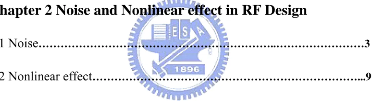
(13) Chapter 2 Noise and Nonlinear effect in RF Design 2.1 Noise Noise is usually generated by the random motions of charges or charge carriers in devices and materials. Because the noise process is random, one cannot identify a specific value of voltage at a particular time, and the only recourse is to characterize the noise with statistical measures, such as the mean-square or root-mean-square values. Because of having various noise sources in the circuit, we need to simplify calculation of the total noise at the output [2]. Obviously, the output-referred noise does not allow a fair comparison of the performance of different circuits because it depends on the gain. According the circuit theory, we can use the input-referred noise of circuits to represent the noise of behavior in the circuits. To overcome the above confusion, we specify the “input-referred noise” of circuits. Illustrate conceptually in Fig. 2-1. To represent the effect of all noise sources in the circuit by a single noise source. The input-referred noise and the input signal are both multiplied by the gain as they are processed by the circuit. Thus, the input-referred noise indicates how much the input signal is corrupted by the circuit’s noise. The input-referred noise is a spurious quantity in that in cannot be measured at the input of the circuit. The two circuits of Figs. 2-1(a) and (b) are equivalent in mathematics but the real physical. 3.
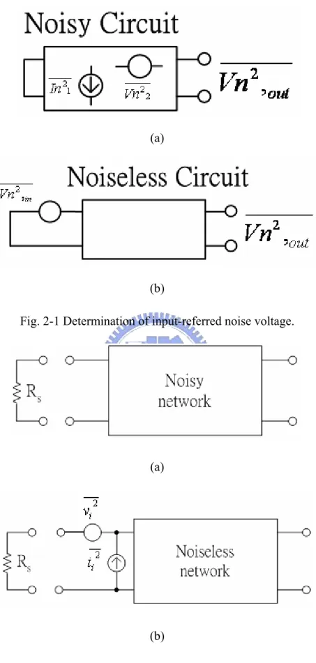
(14) circuit is still that in Fig. 2-1(b). The noise of a two-port network can be modeled by two input noise sources: a series voltage source and a parallel current source. Generally, the correlation between the two sources must be taken into account. The situation is shown in Fig. 2-2, where a two-port network containing noise sources is represented by the same network with internal noise sources removed and with a noise voltage and current source connected at the input. It can be shown that this representation is valid for any source impedance, provided that correlation between the two noise sources is considered [3]. The signal-to-noise ratio (SNR), defined as the ratio of the signal power to the total noise power, is an important parameter. In RF circuit, most of the front-end receiver blocks are characterized in terms of their “noise figure” rather than the input-referred noise. Noise figure has many different definitions. The most commonly accepted definition is noise figure =. SNRin , SNRout. (1). Noise figure is a measure of how much the SNR degrades as the signal passes through a circuit. If a circuit has no noise source, the SNRout = SNRin, regardless of the gain. The noise figure of a two-port amplifier is given by F = Fmin +. 4. rn y s − yopt gs. (2).
(15) where rn = Rn / Z0 is the equivalent normalized noise resistance of the two-port, ys = Rn / Z0 = gs + jbs represents the normalized source admittance, and yop t = gopt+ jbopt represents the normalized source admittance which results in the minimum noise figure, called Fmin. If we express ys and yopt in terms of the reflection coefficients Гs and Гopt. ys =. yopt =. 1 − Γs 1 + Γs. (3). 1 − Γopt. (4). 1 + Γopt. Substitute (3) and (4) into (2) results in the relation F = Fmin +. 4rn Γs − Γopt 2. 2. (1 − Γs ) 1 + Γopt. 2. (5). When Гs=Гopt occurs, the value of F is equal to Fmin. Fmin is a function of the device bias current and operating frequency [4]. For a cascade of stages, the overall noise figure can be obtained in terms of the NF and gain of each stage. For m-stages, the NFtot is equal to NFtot = 1 + ( NF1 − 1) +. NFm − 1 NF2 − 1 +L+ Ap1 Ap1 L Ap ( m−1). (6). where Apm is the available power gain of the m-th stage. This is called the Friis equation. The Friis equation indicates that the noise contributed by each stage decreases as the gain preceding the stage increases, implying that the first few stages in a cascade are the most critical [1].. 5.
(16) (a). (b) Fig. 2-1 Determination of input-referred noise voltage.. (a). (b) Fig. 2-2 Representation of noise in a two-port network by equivalent input voltage and current sources. 6.
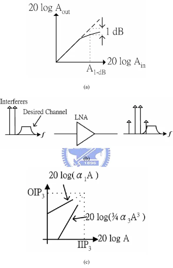
(17) 2.2 Nonlinear effect While many RF circuits can be approximated with a linear model to obtain their response to small signals, nonlinearities often lead to interesting and important phenomena. For simplicity, we assume that. y (t ) ≈ α1 x(t ) + α 2 x 2 (t ) + α 3 x 3 (t ). (7). If a sinusoid is applied to a nonlinear system, the output generally exhibits frequency components that are integer multiples of the input frequency. If x (t ) = A cos ωt , then. y (t ) = α1 A cos ωt + α 2 A2 cos 2 ωt + α 3 A3 cos 3 ωt =. α 2 A2 2. ⎛ 3α 3 A 3 ⎞ α 3 A3 α 2 A2 ⎟⎟ cos ωt + + ⎜⎜ α 1 A + cos 2ωt + cos 3ωt 4 2 4 ⎝ ⎠. (8). (9). In Eq. (9), then term with the input frequency is called the “fundamental” and the higher-order terms the “harmonics.” The amplitude of the nth harmonic consists of a term proportional to An.. 3α 3 A 2 , the gain is therefore a In (9) this occurs if α 3 <0. Written as α 1 + 4 decreasing function of A. In most circuits, the output is a “compressive” or “saturating” function of the input; that is, the gain approached zero for sufficiently high input levels. This effect is quantified by the “1-dB compression point,” defined as the input signal level that causes the small-signal gain to drop by 1 dB. If plotted on a log-log scale as a function of the input level, the output level falls below its ideal 7.
(18) value by 1 dB at the 1-dB compression point. When two signals with different frequencies are applied to a nonlinear system, the output in general exhibits some components that are not harmonics of the input frequencies. Called intermodulation (IM), this phenomenon arises from multiplication of the two signals when their sum is raised to a power greater than unity. We assume that. x(t ) = A1 cos ω1t + A2 cos ω2t. (10). Thus,. y(t ) = α1 ( A1 cosω1t + A2 cosω2t ) + α 2 ( A1 cosω1t + A2 cosω2t )2 (11). + α 3( A1 cosω1t + A2 cosω2t )3. Expanding the left side and discarding DC terms and harmonics, we obtain the intermodulation products:. 3α A A 3α A A ω → 2ω1 ± ω 2 : 3 1 2 cos(2ω1 + ω 2 )t + 3 1 2 cos(2ω1 − ω 2 )t 4 4. (12). 3α A A 3α A A ω → 2ω 2 ± ω1 : 3 2 1 cos(2ω 2 + ω1 )t + 3 2 1 cos(2ω 2 − ω1 )t 4 4. (13). 2. 2. 2. 2. Because the difference between ω1 and ω2 is small, the components at 2ω1-ω2 and 2ω2-ω1 appear in the vicinity of ω1 and ω2. In a typical two-tone test, A1=A2=A, and the ratio of the amplitude of the output third-order products to α 1A. defines the IM distortion. If a weak signal accompanied by two strong interferers. experiences third-order nonlinearity, then one of the IM products falls in the band of 8.
(19) interest, corrupting the desired component. Use IP3 to characterize this behavior. Called the “third intercept point” (IP3), this parameter is measured by a two-tone test in which A is chosen to be sufficiently small so that higher-order nonlinear terms are negligible and the gain is relatively constant and equal to α1. The third-order intercept point is defined to be at the intersection of the two lines [1].. 9.
(20) (a). (b). (c) Fig. 2-3 (a) Definition of the 1-dB compression point, (b) Corruption of a signal due to intermodulation, (c) The third-order intercept point.. 10.
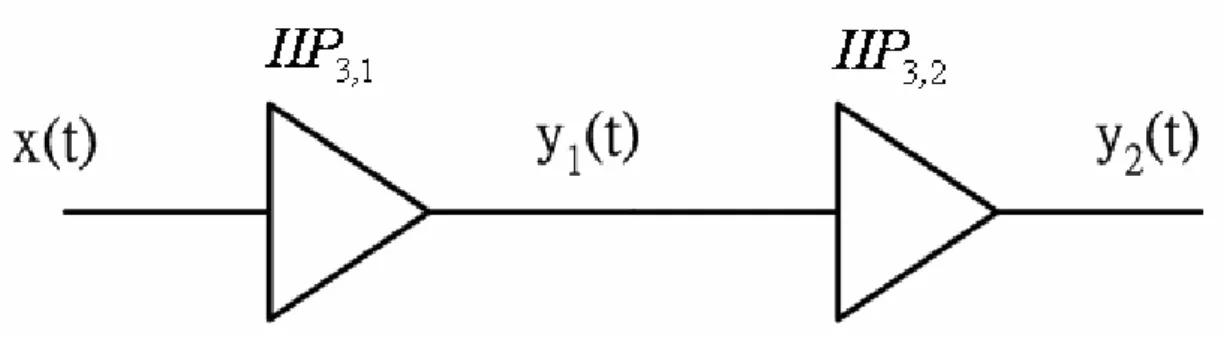
(21) 2.3 Cascaded Nonlinear Stages Since in RF systems, signals are processed by cascaded stages, it is important to know how the nonlinearity of each stage is referred to the input of the cascade. Consider two nonlinear stages in cascade. As shown in Fig.2-4. Assuming that the input-output relationship is. y1 (t ) = α1 x(t ) + α 2 x 2 (t ) + α 3 x 3 (t ). (14). y2 (t ) = β1 y1 (t ) + β 2 y1 (t ) + β 3 y1 (t ). (15). 2. 3. Substitute (14) into (15) results in the relation. y2 (t ) = α1β1 x(t ) + (α 3 β1 + 2α1α 2 β 2 + α1 β 3 ) x 3 (t ) 3. (16). If we consider only the first- and third-order terms, then AIP 3 =. 4 α 1 β1 . 3 α 3 β1 + 2α1α 2β 2 + α13 β 3. (17). From equation (17) can be simplified if the two sides are inverted and squared: 1 A2 IP 3. =. 1 A2 IP 3,1. α 3α 2 β 2 + 21 , 2β 1 A IP 3, 2 2. +. (18). where AIP3,1 and AIP3,2 represent the input IP3 points of the first and second stages, respectively. From the above result, we note that as α1 increases, the overall IP3 decreases. This is because with higher gain in the first stage, the second stage senses larger input levels, thereby producing much greater IM3 products [1].. 11.
(22) Fig. 2-4 Cascaded nonlinear stages.. 12.
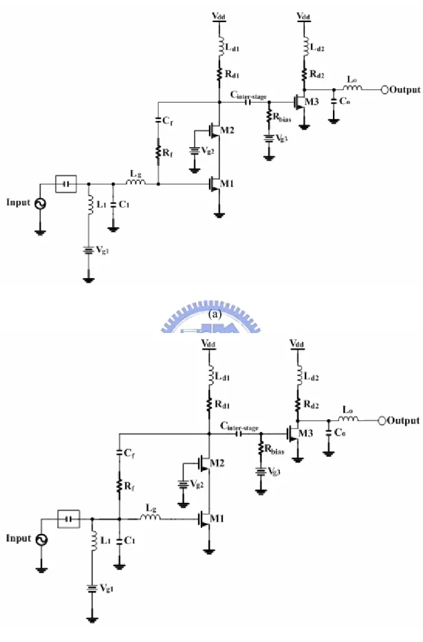
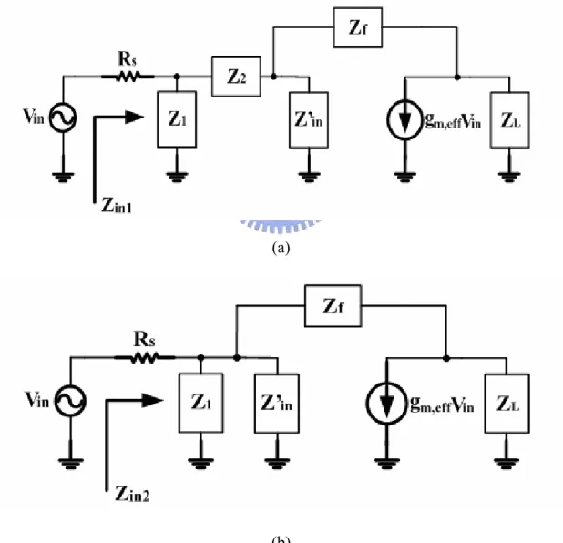
(23) Chapter 3 Design of UWB LNA with cascode feedback structure 3.1 Circuit topology In designing a broadband amplifier, feedback and distributed configuration are most widely used. In the chapter, feedback configuration was used instead of distributed configuration because it is more adequate for integration due to better uniformity and stability at frequencies below 12GHz. In addition, the cascode structure has been considered as the best topology for wideband applications because of its advantages [11]. We design UWB LNA with cascode R-C feedback structure. There are two types in this structure. The feedback1 structure is the R-C feedback connected between Lg and MOS1’s gate, like Fig. 3-1(a). The feedback2 structure is the R-C feedback connected between input and Lg, like Fig. 3-1(b). From Fig. 3-1 (a) and (b), we can observe that they are two stage low noise amplifier. First stage used the cascode R-C feedback structure. The advantages of cascode structure are high gain, wider bandwidth, better stability and reverse isolation. The cascode configuration is being used to reduce the high frequency roll-off of the input devices due to the Miller effect [11]. It can also be performed the input/output matching independently. The R-C feedback (Rf & Cf) in cascode circuit improves the. 13.
(24) S11 of the circuit and stabilizes the common-gate without reducing the gain. Above all, it can satisfy the requirements of wideband system for both noise and power simultaneously by carefully feedback resistance. The MOS M1 dominates the noise performance. These two MOS (M1 and M2) have little effects with each other. The two LNA (feedback1 and feedback2) for UWB applications were designed using TSMC 0.18um RF CMOS technology.. 14.
(25) (a). (b) Fig. 3-1 Proposed UWB LNA schematic (a) feedback1, (b) feedback2.. 15.
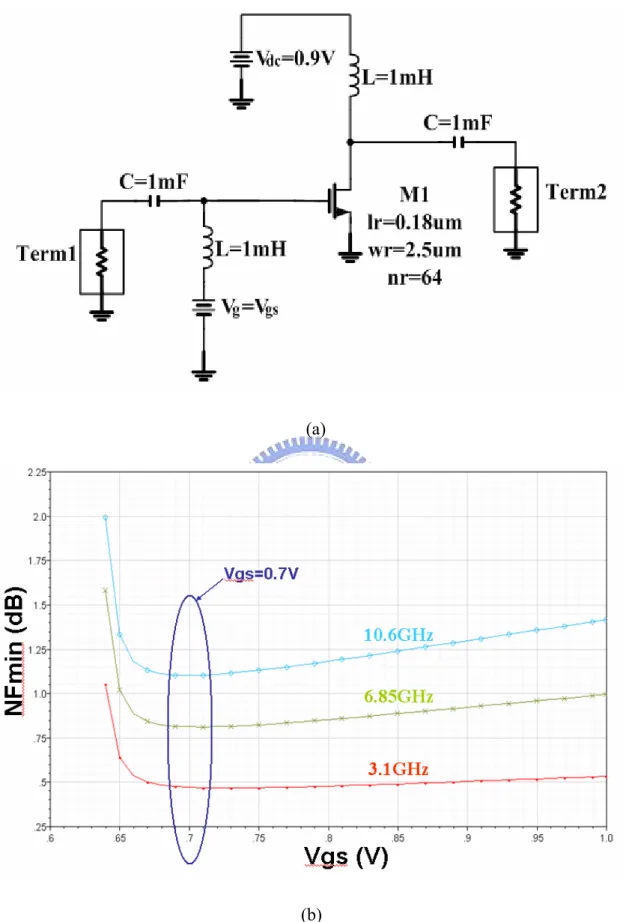
(26) 3.2 Design procedures 3.2.1 Transistor sizing and bias condition Since the size of transistor and bias condition determine the power dissipation, it is often recommended to decide them with a certain power budget. However, we should evaluate the size of the transistor versus bias condition carefully, because they are also related to the impedance seen by the input gate. Thus, the first choice is to determine the size and bias condition that satisfies both impedance and noise matching with limited bias current. Fig. 3-2(a) shows a simulation circuit of MOS NFmin. In Fig. 3-2(a), the input transistor M1 (W/L = 160/0.18 um) is chose and is biased at 7.5mA. In Fig. 3-1(a) and (b), the size of the cascode transistor M2 (W/L = 64/0.18 um) is decided considering a trade-off between gain (S21) and -3dB bandwidth. The size of the second stage transistor M3 is W/L = 64/0.18 um. The total power consumption is 18.8mW. Fig. 3-2(b) shows the Vgs versus NFmin at 3.1GHz, 6.85GHz and 10.6GHz. From Fig. 3-2(b), we can observe that when Vgs = 0.7V, the transistor M1 has the minimum noise figure. Thus, the bias condition is decided to Vgs = 0.7V.. 16.
(27) (a). (b) Fig. 3-2 (a) Simulation circuit of MOS NFmin, (b) Vgs v.s. NFmin at 3.1GHz、 6.85GHz and 10.6GHz. 17.
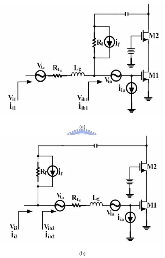
(28) 3.2.2 Noise analysis The noise performance of the R-C cascode feedback topology is determined by three main contributors: the feedback resistor Rf, the gate inductor Lg and the noise of the amplifying device M1. The optimization of the noise contribution from M1 relies on the choice of its width for a given bias current. MOS transistor noise sources are shown in Fig. 3-3(a). The noise generator i 2 d is I aD ⎛2 ⎞ i 2 d = 4kT ⎜ g m ⎟Δf + k Δf f ⎝3 ⎠. (19). I aD ⎛2 ⎞ Δf is flicker noise where 4kT ⎜ g m ⎟Δf is thermal noise component, and k f ⎝3 ⎠. component. And noise generator i 2 g is i 2 g = 2qI G Δf. (20). The input-referred in a conventional way and replaced with two correlated noise generators, as shown in Fig. 3-3(b), because the current gain of the source degeneration is β ( jω ) =. g ωT , and the cutoff frequency is ωT ≈ m , so the i 2 ia is jω C gs jωC gs 2 2 2. i. ia. =i. g. +. gm. i. d. (21). and v 2 ia is v 2 ia =. i2d gm. (22). Fig. 3-4(a) and (b) show the equivalent circuit of the input stage for noise calculation. 18.
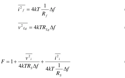
(29) In Fig. 3-4(a), the feedback1 topology: vib1 = via. (23). iib1 = iia + i f. (24). vi1 = vib1 + iib1 ⋅ R Lg + v Lg = via + iia ⋅ RLg + v Lg + i f ⋅ RLg. (25). ii1 = iib1 = iia + i f. (26). Then,. Thus, the total equivalent noise voltage and current of feedback1 is 2. v 2 i1 = v 2 ia + v 2 Lg + i 2 ia ⋅ RLg + i 2 f ⋅ RLg. 2. i 2 i1 = i 2 ia + i 2 f. (27) (28). In Fig. 3-4(b), the feedback2 topology:. vib 2 = via + iia ⋅ RLg + v Lg. (29). iib 2 = iia. (30). vi 2 = vib 2 = via + iia ⋅ R Lg + v Lg. (31). ii 2 = iib 2 + i f = iia + i f. (32). Then,. Thus, the total equivalent noise voltage and current of feedback2 is. v 2 i 2 = v 2 ia + v 2 Lg + i 2 ia ⋅ RLg i 2 i 2 = i 2 ia + i 2 f. where. 19. 2. (33) (34).
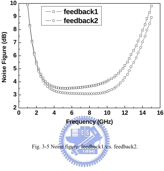
(30) 1 Δf Rf. (35). v 2 Lg = 4kTRLg Δf. (36). v 2i + 4kTRS Δf. (37). i 2 f = 4kT. The noise factor is F = 1+. i 2i 1 Δf 4kT RS. From equation (27) and (33), we can observe that the total noise of feedback1 is greater than feedback2 due to the i. ⋅ RLg item. Fig. 3-5 shows the noise figure: 2. 2 f. feedback1 versus feedback2. We can observe that the noise figure of feedback2 topology is better than feedback1.. (a). (b) Fig. 3-3 Noise model for the amplifying transistor M1 (a) M1 noise sources, (b) Input-referred equivalent noise generators. 20.
(31) (a). (b) Fig. 3-4 Equivalent circuit of the input stage for noise calculation (a) feedback1, (b) feedback2.. 21.
(32) 10. feedback1 feedback2. Noise Figure (dB). 9 8 7 6 5 4 3 2. 0. 2. 4. 6 8 10 Frequency (GHz). 12. Fig. 3-5 Noise figure: feedback1 v.s. feedback2.. 22. 14. 16.
(33) 3.2.3 Input and output match Input matching: In feedback1 topology, the small signal equivalent is shown in Fig. 3-6(a), where Z 'in = 1. sC gs1. Z 1 = sL1 // 1. sC1. (38) (39). Z 2 = sL g. (40). g m,eff ≅ g m1 × 1 = g m1. (41). Z L = Rd 1 + sLd 1. (42). Z f = Rf + 1. sC f. (43). For this configuration, the input impedance and the gain can be calculated to be ⎡ ⎤ Z 'in ⋅Z f Z in1 = ⎢ + Z 2 ⎥ // Z 1 ⎣⎢ Z f + ( AV − 1) ⋅ Z 'in ⎦⎥ AV 1 =. Z L + g m ,eff ⋅ Z f ⋅ Z L ZL − Z f. (44). (45). And in feedback2 topology, the small signal equivalent is shown in Fig. 3-6(b), where Z 'in = sL g + 1. sC gs1. (46). Z 1 , Z L , Z f and g m,eff are the same with feedback1. For this configuration,. the input impedance and the gain can be calculated to be ⎡ ⎤ Z 'in ⋅Z f Z in 2 = ⎢ ⎥ // Z 1 ⎣⎢ Z f + ( AV − 1) ⋅ Z 'in ⎦⎥ 23. (47).
(34) AV 2 =. Z L + g m ,eff ⋅ Z f ⋅ Z L ZL − Z f. (48). Since the circuit parameters Z 'in and AV are frequency dependant, the characteristics of Z f will vary accordingly over the frequency band. Thus, select Z f and combination of R 、 C components , perfect matching and gain can be achieved. Output matching: The second stage is decided to use L-C section for output match.. (a). (b) Fig. 3-6 (a) Feedback1 configuration, (b) Feedback2 configuration.. 24.
(35) 3.2.4 Shunt peaking A model of shunt peaking amplifier is shown in Fig. 3-7(a). The capacitance C may be taken to represent all the loading on the output node, including that of a subsequent stage. The resistance R is the effective load resistance at that node and the inductor provides the bandwidth enhancement. It’s clear from the model that the transfer function. vout. iin. is just the impedance of the RLC network, so it should be. straightforward to analyze. The addition of an inductance in series with the load resistor provides an impedance component that increases with frequency, which helps offset the decreasing impedance of the capacitance, leaving net impedance that remains roughly constant over a broader frequency range than that of the original RC network. The impedance of the RLC network may be written as. Z ( s ) = (sL + R ) //. 1 R[ s ( L / R)] + 1 = 2 sC s LC + sRC + 1. (49). The load is designed to achieve flat gain over the whole bandwidth. The choice of Ld is determined by two opposite requirements: Ld must be sizable to have large gain and must be small so that it resonates C out out of band [9]. Rd is chosen to place the zero frequency ( ω z =. Rd. Ld. ) as close as to the lower edge of the band to. improve the gain. We choose Rd = 90Ω and Ld = 1.7nH so that ω z ≅ 8.5GHz . The shunt peaking is shown in Fig. 3-7(b).. 25.
(36) (a). Fig. 3-7 (a) Model of shunt-peaked amplifier, (b) Gain compare with shunt-peaking.. 26.
(37) 3.3 Simulation and Measurement Result Fig. 3-8 shows the s-parameters of simulation and measurement in feedback1 and feedback2. Fig. 3-9 shows the noise figure and Fig. 3-10 shows the linearity. Fig. 3-11 is the die photo. In feedback1, the forward gain (S21) is less than simulation about 5dB due to the L1 without connecting bypass capacitors and process variation. When measured, the Vg1 dc probe without bypass capacitors may cause signal loss and have parasitical effects so that the gain is less than simulation. And, the ripple in 3 to 6GHz is due to the M2’s gate bypass capacitor layout which cause parasitic inductor and capacitor resonated in 3 to 6GHz. The reverse isolation (S12) is below -32 dB. The magnitude of S11 is below -7.5dB and S22 is below -10dB in entire operation frequency band. The S12, S11 and S22 are very close to the simulation result. The average noise figure is about 8dB and the minimum noise figure is 6.7dB at 5GHz. The IIP3 is 2dBm at 5.5GHz. The total power consumption is about 18mW with a power supply of 1.8 volts. And the die area including the pads is 0.77 mm2. In feedback2, the forward gain (S21) is less than simulation about 2dB due to the L1 without connecting bypass capacitors. The reason is the same with feedback1. And, the ripple in 3 to 6GHz is also the same, because their basic structure and layout are slightly different. The reverse isolation (S12) is below -45 dB. The magnitude of S11 is. 27.
(38) below -7.2dB and S22 is below -8.2dB in entire operation frequency band. The S12, S11 and S22 are very close to the simulation result. The noise figure is very flat about 5.5dB and the minimum noise figure is 4.55dB at 9GHz. The IIP3 is -2dBm at 5.5GHz. The total power consumption is about 18mW with a power supply of 1.8 volts. And the die area including the pads is 0.77 mm2. From feedback1 and feedback2 structure, we can observe that the noise figure in feedback2 is better than feedback1 and the gain is also better. By the feedback2 structure, a low power, low noise amplifier can be achieved.. 3.1~10.6. Gain. NF. S11. S22. IIP3. Pdc. (GHz). (dB). (dB). (dB). (dB). (dBm). (mW). Feedback1. 5. 8. <-7.5. <-10. 2. 18. Feedback2. 9. 5.5. <-7.2. <-8.2. -2. 18. Table 3.1 Measurement results summary.. 28.
(39) 20. simulation measurement. feedback1 15. S21 (dB). 10 5 0 -5 -10 -15. 0. 2. 4. 6. 8. 10. 12. 14. 16. Frequency (GHz). 20. simulation measurement. feedback2. S21 (dB). 15. 10. 5. 0. 0. 2. 4. 6. 8. 10. Frequency (GHz). (a). 29. 12. 14. 16.
(40) 0. simulation measurement. feedback1. S12 (dB). -20. -40. -60. -80. 0. 2. 4. 6. 8. 10. 12. 14. 16. Frequency (GHz). 0. simulation measurement. feedback2. S12 (dB). -20. -40. -60. -80. 0. 2. 4. 6. 8. 10. Frequency (GHz). (b). 30. 12. 14. 16.
(41) 5. simulation measurement. feedback1 0. S11 (dB). -5 -10 -15 -20 -25. 0. 2. 4. 6. 8. 10. 12. 14. 16. Frequency (GHz). 5. simulation measurement. feedback2. 0. S11 (dB). -5 -10 -15 -20 -25 -30 -35. 0. 2. 4. 6. 8. 10. Frequency (GHz). (c). 31. 12. 14. 16.
(42) 5. simulation measurement. feedback1. S22 (dB). 0. -5. -10. -15. -20. 0. 2. 4. 6. 8. 10. 12. 14. 16. Frequency (GHz). 0. simulation measurement. feedback2. S22 (dB). -5. -10. -15. -20. 0. 2. 4. 6. 8. 10. 12. 14. 16. Frequency (GHz). (d) Fig. 3-8 S-parameters of feedback1 and feedback2 (a) S21, (b) S12, (c) S11, (d) S22.. 32.
(43) 30. simulation measurement. feedback1 Noise Figure (dB). 25 20 15 10 5 0. 0. 2. 4. 6. 8. 10. 12. 14. 16. Frequency (GHz). 20. simulation measurement. Noise Figure (dB). feedback2 15. 10. 5. 0. 0. 2. 4. 6. 8. 10. 12. 14. Frequency (GHz). Fig. 3-9 Noise figure of feedback1 and feedback2.. 33. 16.
(44) 10. Output Power (dBm). 0. feedback1. -10 -20 -30 -40 -50 -60 -70 -80 -90 -100 -35. -30. -25. -20. -15. -10. -5. 0. 5. Input Power (dBm). 10. Output Power (dBm). 0. feedback2. -10 -20 -30 -40 -50 -60 -70 -80 -30. -25. -20. -15. -10. -5. 0. Input Power (dBm). Fig. 3-10 Linearity of feedback1 and feedback2. 34. 5.
(45) (a). (b) Fig. 3-11 Die photo (a) feedback1, (b) feedback2. 35.
(46) Chapter 4 Design of a low power UWB LNA with current-reused structure 4.1 Circuit topology Fig. 4-1 shows the proposed current-reused high gain two stage amplifier topology. In Fig. 4-1, Rd 1 、 Ld 1 and Ld 2 are the loads for each common-source amplifier, C g 2 is the coupling capacitor, C bypass is the bypass capacitor, and Rbias is the bias resistor. The proposed amplifier is the current-reused cascaded common-source amplifier with capacitive inter-stage coupling except the extra inductor Lg 2 . In Fig. 4-1, the value of Lg 2 is adjusted for the series resonance with the input capacitance of the second stage. Accordingly, the first stage is designed to resonate at the lower bound of the frequency band. The second stage, on the other hand, resonates at the higher bound of the frequency band. To achieve the goal of power saving, the second stage is stacked on top of the first stage. A coupling capacitor and a bypass capacitor are required for this topology. The capacitor C g 2 provides signal coupling between the two stages and the capacitor C bypass functions as an ac ground at the source of transistor M2. The capacitance of capacitor C bypass is chosen to be as large as possible to provide ideal ac ground in conventional narrow band designs as well.. 36.
(47) Fig. 4-1 Proposed UWB LNA schematic.. 37.
(48) 4.2 Design procedures 4.2.1 Transistor sizing and bias condition Since the size of transistor and bias condition determine the power dissipation, it is often recommended to decide them with a certain power budget. However, we should evaluate the size of the transistor versus bias condition carefully, because they are also related to the impedance seen by the input gate. Thus, the first choice is to determine the size and bias condition that satisfies both impedance and noise matching with limited bias current. Fig. 4-2(a) shows a simulation circuit of MOS NFmin. In Fig. 4-2(a), the input transistor M1 (W/L = 78/0.18 um) is chose and is biased at 3.89mA. In Fig. 4-1, the size transistor M2 (W/L = 80/0.18 um) is decided. The bias current for M3 is selected to be 1.2mA and the width of M3 is 88 um. The transistor used to implement the current source is 24 um width. The total power consumption is only 9.1mW. Fig. 4-2(b) shows the Vgs versus NFmin at 3.1GHz, 6.85GHz and 10.6GHz. From Fig. 4-2(b), we can observe that when Vgs = 0.7V, the transistor M1 has the minimum noise figure. Thus, the bias condition is decided to Vgs = 0.7V.. 38.
(49) (a). (b) Fig. 4-2 (a) Simulation circuit of MOS NFmin, (b) Vgs v.s. NFmin at 3.1GHz、 6.85GHz and 10.6GHz.. 39.
(50) 4.2.2 Input and output match Input matching: Fig. 4-3 shows the small signal model of the input impedance. The passive components L1、C1、L2 、C 2 、L g1 and LS are adopted for matching network at the input to resonate over the entire frequency band. The source inductor LS is used to generate a real term for input impedance matching. g m1 LS / C gs1 = RS = 50Ω. (50). The input impedance is derived as Z 2 ( Z 3 + ω T LS ) Z 2 + Z 3 + ω T LS. (51). Z 1 = sL1 +. 1 sC1. (52). Z 2 = sL2 //. 1 sC 2. (53). Z in = Z 1 +. where. Z 3 = s ( L3 + LS ) +. ωT =. 1 sC gs1. g m1 C gs1. (54) (55). Output matching: Fig. 4-4 shows the output matching network. The buffer must drive a 50Ω external load. The buffer is independently biased by means of a current source made up of two transistors in current mirror configuration. 1 = 50Ω g m3 40. (56).
(51) Fig. 4-3 Small signal model of the input impedance.. Fig. 4-4 Output matching network.. 41.
(52) 4.2.3 Gain analysis Fig. 4-5(a) shows the current-reused two stage cascade amplifier with series inter-stage resonance. In Fig. 4-5(a), the value of Lg 2 is adjusted for the series resonance with the input capacitance of the second stage. Fig. 4-5(b) shows the small signal equivalent circuit for the portion of the circuit enclosed by the dashed box in Fig. 4-5(a) in order to estimate the current gain from the drain of M1 to that of M2. In Fig. 4-5(b), Z d 1 represents the load of M1 equal to R Lg 2 is the parasitic series resistance of Lg 2 . The V gs 2 and g m 2 represent the gate-to-source voltage and the transconductance of M2. The current-amplifying characteristic of the series inter-stage resonated amplifier can be understood by analyzing the circuit shown in Fig. 4-5(b). From Fig. 4-5(b), the current gain id 2. id1. can be expressed as. g Z d1 id 2 = m2 × id1 sC gs 2 Z d 1 + sL g 2 + (1 / sC g 2 + 1 / sC gs 2 ) + RLg 2. (57). From equation (57), L g 2 resonates with 1 / sC g 2 + 1 / sC gs 2 at high frequency band. If Z d 1 provides sufficiently high impedance, Z d 1 >> RLg 2 , then, id 2. id 1. ≅. g m2. sC gs 2. ,. equation (1) can be approximated as g id 2 ω ≅ m2 ≅ T id1 sC gs 2 ω. where ωT is M2’s cutoff frequency, ω is the frequency of operation.. 42. (58).
(53) (a). (b) Fig. 4-5 (a) Current-reused two stage cascade amplifier with series inter-stage resonance, (b) Small signal equivalent representation of the circuit from node X to Y.. 43.
(54) 4.2.4 Shunt peaking The load inductor of the first stage, Ld 1 , is chosen to resonate at 3GHz with the Rd 1 at the drain node of the transistor M1. The load of inductor of the second stage is chosen to generate a resonance at 10 GHz. As shown in Fig. 4-6, a flat frequency response can be obtained by the combination of the resonance of the first and second stages ( ω z1 ≅ 3GHz and ω z 2 ≅ 10GHz ). To fit the frequency bands of UWB applications, the -3dB bandwidth is designed to cover 3.1 – 10.6 GHz.. 20. S21 (dB). 10. 0. -10 total gain 1st-stage resonance 2nd-stage resonance. -20. -30. 0. 2. 4. 6 8 10 Frequency (GHz). 12. 14. Fig. 4-6 1st-stage and 2nd-stage resonance contribute to gain.. 44. 16.
(55) 4.3 Simulation and Measurement Result Fig. 4-7 shows the s-parameters of simulation and measurement. Fig. 4-8 shows the noise figure and Fig. 4-9 shows the linearity. Fig. 4-10 is the die photo. In the current-reused structure, the forward gain (S21) is less than simulation about 2dB due to the L2 without connecting bypass capacitors. When measured, the Vg1 dc probe without bypass capacitors may cause signal loss and have parasitical effects so that the gain is less than simulation. The reverse isolation (S12) is below -50 dB. The magnitude of S11 is below -8.6dB and S22 is below -8dB in entire operation frequency band. The S12 , S11 and S22 are very close to the simulation result. The average noise figure is about 5.2dB and the minimum noise figure is 4.87dB at 8GHz. The IIP3 is -13dBm at 5.5GHz. The total power consumption is only 9.4mW with a power supply of 1.8 volts. And the die area including the pads is 0.98 mm2. By current-reused method, a high gain, low power, low noise amplifier can be achieved. It only consumes 9.4mW.. 3.1~10.6. Gain. NF. S11. S22. IIP3. Pdc. (GHz). (dB). (dB). (dB). (dB). (dBm). (mW). Current-reused. 9. 5.2. <-8.6. <-8. -13. 9.4. Table 4.1 Measurement results summary.. 45.
(56) 20. simulation measurement. S21 (dB). 10. 0. -10. -20. 0. 2. 4. 6. 8. 10. 12. 14. 16. Frequency (GHz). (a). 0. simulation measurement. S12 (dB). -20. -40. -60. -80. -100. 0. 2. 4. 6. 8. 10. Frequency (GHz). (b). 46. 12. 14. 16.
(57) 10. simulation measurement. S11 (dB). 0. -10. -20. -30. -40. 0. 2. 4. 6. 8. 10. 12. 14. 16. Frequency (GHz). (c). 0. simulation measurement. S22 (dB). -5. -10. -15. -20. 0. 2. 4. 6. 8. 10. 12. 14. Frequency (GHz). (d) Fig. 4-7 S-parameters (a) S21, (b) S12, (c) S11, (d) S22. 47. 16.
(58) 30. simulation measurement. Noise Figure (dB). 25 20 15 10 5 0. 0. 2. 4. 6. 8. 10. 12. 14. 16. Frequency (GHz). Fig. 4-8 Noise figure.. 0. Output Power (dBm). -10 -20 -30 -40 -50 -60 -70 -80 -90 -100 -45. -40. -35. -30. -25. Input Power (dBm). Fig. 4-9 Linearity. 48. -20. -15. -10.
(59) Fig. 4-10 Die photo.. 49.
(60) Chapter 5 Summary We design UWB LNA with R-C feedback structure in feedback1 and feedback2 and a low power current-reused structure. From measurement results, we can observe that feedback2 has better noise performance than feedback1 and current-reused structure is not only low power but also has good noise performance. Table 5-1 is the comparison of broadband LNA performance. We can find out feedback2 has good noise performance and current-reused structure has very low power consumption and good noise figure. Ref.. [9]. Feedback1. Feedback2. Currentreused. B.W.. Gain. NF. S11. S22. IIP3. Pdc. Tech.. (GHz). (dB). (dB). (dB). (dB). (dBm). (mW). CMOS. (max). (average). 9. 4~9. < -9. < -20. -6.7. 18. .18. 2004. (9.3). (6.5). 5. 7.7~8.7. (6). (8). 9. 5.9~4.8. (10.5). (5.5). 9. 5.6~5. (11.9). (5.2). 2.4~9.5. 3.1~10.6. 3.1~10.6. 3.1~10.6. year. *9 < -7.5. < -10. 2. 18. .18. 2006. <-7.2. <-8.2. -2. 18. .18. 2006. < -8.6. < -8. -13. 9.4. .18. 2006. *7. Table 5.1 Comparison of broadband LNA performance. 50. * LNA core only.
(61) Reference [1] B. Razavi, “RF Microelectronics,” 1st ed. NJ, USA: Prentice-Hall PTR, 1998. [2] T. H. Lee, “The Design of CMOS Radio-Frequency Integrated Circuits,” 1st ed. New York: Cambridge Univ. Press, 1998. [3] B. Razavi, “Design of Analog CMOS Integrated Circuits,” International ed. NY: McGraw Hill Co. 2001. [4] G. Gonzalez, “Microwave Transistor Amplifiers Analysis and Design,” 2nd ed. NJ: Prentice-Hall, Inc. 1997. [5] Park, Y.; Lee, C.-H.; Cressler, J.D.; Laskar, J.; Joseph, A.; “A very low power SiGe LNA for UWB application,” IEEE MTT-S Int. Microwave Symp. Dig, Page(s):4 pp, June 2005. [6] Ghosh, P.P.; Enjun Xiao; “Design of a New CMOS Low Noise Amplifier for Ultra Wide-Band Wireless Receiver in 0.18μm technology,” IEEE International Conference, pp. 514-519, Sept. 2005. [7] Sung-Huang Lee; Ying-Zong Juang; Chin-Fong Chiu; Hwann-Kaeo Chiou; “A novel low noise design method for CMOS L-degeneration cascoded LNA,” IEEE Asia-Pacific Conference Circuit and System ,Dec. 2004, pp. 273-276 vol.1. [8] Wei Guo; Daquan Huang; “Noise and linearity analysis for a 1.9 GHz CMOS LNA,” IEEE APCCAS . Dig., pp. 409 - 414 vol.2,Oct. 2002.. 51.
(62) [9] Bevilacqua, A.; Niknejad, A.M.; “An ultrawideband CMOS low-noise amplifier for 3.1-10.6-GHz wireless receivers,” IEEE JSSC, pp. 2259 - 2268,Dec. 2004. [10] Chang-Wan Kim; Min-Suk Kang; Phan Tuan Anh; Hoon-Tae Kim; Sang-Gug Lee; “An ultra-wideband CMOS low noise amplifier for 3-5-GHz UWB system,” IEEE JSSC, pp. 544 - 547,Feb. 2005. [11] Heechan Doh; Youngkyun Jeong; Sungyong Jung; Youngjoong Joo; “Design of CMOS UWB low noise amplifier with cascode feedback,” IEEE MWSCAC, pp. 641-644 vol.2,July 2004. [12] Jose, S.; Hyung-Jin Lee; Dong Ha; Choi, S.S.; “A low-power CMOS power amplifier for ultra wideband (UWB) applications,” IEEE ISCAS, pp. 5111-5114 Vol.5, May 2005. [13] Hyung-Jin Lee; Dong Sam Ha; Choi, S.S.; “A systematic approach to CMOS low noise amplifier design for ultrawideband applications,” IEEE ISCAS, pp. 3962-3965 Vol.4, May 2005. [14] Chang-Ching Wu; Mei-Fen Chou; Wen-Shen Wuen; Kuei-Ann Wen; “A low power CMOS low noise amplifier for ultra-wideband wireless applications,” IEEE ISCAS, pp. 5063–5066 Vol.5,May 2005. [15] Taris, T.; Begueret, J.B.; Lapuyade, H.; Deval, Y.; “A 3-10 GHz 0.13/spl mu/m CMOS body effect reuse LNA for UWB applications,” IEEE NEWCAS, pp.. 52.
(63) 361–364, June 2005. [16] Choong-Yul Cha; Sang-Gug Lee; “A 5.2-GHz LNA in 0.35-/spl mu/m CMOS utilizing inter-stage series resonance and optimizing the substrate resistance,” IEEE JSSC, pp. 669–672, April 2003.. 53.
(64) Vita 姓名:張國慶 性別:男 出生年月日:民國71年7月15日 籍貫:台灣省彰化縣 住址:彰化縣溪湖鎮湖東里向上路35號 學歷:國立中山大學電機工程學系 (89年9月~93年6月) 國立交通大學電子研究所固態電子組 (93年9月入學). 論文題目: 應用於超寬頻3.1-10.6GHz無線接收端之疊接回授架構與低功率電流再使用架構 之低雜訊放大器之設計. (Design of a cascode feedback and a low power current-reused LNA for Ultra-wideband 3.1 to 10.6GHz Wireless Receivers). 54.
(65)
數據
+7
Outline
相關文件
低於 5 萬元 國際驗證申請費之 30 %之費用優惠,並以 1 萬元為上限 5~10 萬元 國際驗證申請費之 30 %之費用優惠,並以 3 萬元為上限.. 高於 10 萬元
1.提高接收資料的速度 2.降低資料傳輸速度 接收端RX接收資料的速度低於發.
Zhang, “Novel Microstrip Triangular Resonator Bandpass Filter with Transmission Zeros and Wide Bands Using Fractal-Shaped Defection,” Progress In Electromagnetics Research, PIER
接收器: 目前敲擊回音法所採用的接收 器為一種寬頻的位移接收器 其與物體表
油壓開關之動作原理是(A)油壓 油壓與低壓之和 油壓與低 壓之差 高壓與低壓之差 低於設定值時,
請繪出交流三相感應電動機AC 220V 15HP,額定電流為40安,正逆轉兼Y-△啟動控制電路之主
首先,在前言對於為什麼要進行此項研究,動機為何?製程的選擇是基於
Abstract - A 0.18 μm CMOS low noise amplifier using RC- feedback topology is proposed with optimized matching, gain, noise, linearity and area for UWB applications.. Good
