國 立 交 通 大 學
電 機 與 控 制 工 程 研 究 所
碩 士 論 文
應用於溼度感測器之
低電壓低功率三角積分調變器
The Design of a Low-Voltage, Low-Power
Sigma-Delta Modulator
For Humidity Sensors
研 究 生:張智琦
指導教授:蘇朝琴 教授
應用於溼度感測器之低電壓低功率三角積分調變器
The Design of Low-Voltage, Low-Power
Sigma-Delta Modulator for Humidity Sensors
研 究 生:張智琦 Student
:
Chih-Chi
Chang
指導教授:蘇朝琴 教授
Advisor : ChauChin Su
國 立 交 通 大 學
電 機 與 控 制 工 程 研 究 所
碩 士 論 文
A Thesis
Submitted to Department of Computer and Information Science College of Electrical Engineering and Computer Science
National Chiao Tung University In partial Fulfillment of the Requirements
for the Degree of Master
in
Electrical and Control Engineering October 2006
Hsinchu, Taiwan, Republic of China
變器
研究生:張智琦 指導教授:蘇朝琴
國立交通大學電機與控制工程研究所
摘要
近年來由於積體電路製程的進步以及微機電系統的半導體後製程發展,感測 器被廣泛的應用在許多不同的領域。在環境監控這個應用上,有關無線感測網路 的概念已經被提出來討論。在無線感測網路中,需要低功率消耗的感測器前端電 路來滿足長時間監控的需求。在這篇論文裡,我們實現一個應用在濕度感測器的 超低功率三角積分調變器 這篇論文中提到了有關低電壓、低功率的三角積分調變器的設計技術。利用 切換電容式積分器來實現一個二階的三角積分調變器。為了降低整個系統的功率 消耗,所設計的運算放大器操作在weak inversion,功率消耗只有 200nW。為了降低運算放大器的非理想性效應,電路中使用 correlated double sampling 的技
巧。由於系統操作在1V 的低電壓環境,有關開關的驅動問題以及運算放大器直
流增益的提升都有探討。為了降低clock feedthrough 的問題,所有的 switch 都是
使用NMOS dummy switch。
所提出的電路架構將被實現在TSMC CMOS 0.18µm 的製程,其晶片面積為 m m µ µ 0.37 63 . 0 × (不包含 PAD),當取樣頻率在 6.4k Hz、頻寬被設定在 50Hz 及 電壓為 1V 時,可以得到最大之訊號失真雜訊比(SNDR)為 52.75dB,動態範圍
(Dynamic Range)為 52.39dB。此電路系統總共的功率消耗為 1.5 uW。
The Design of Low-Voltage, Low-Power
Sigma-Delta Modulator for Humidity Sensors
Student: Chih-Chi Chang Advisor: ChauChin Su
Institute of Electrical and Control Engineering
Nation Chiao Tung University
Abstract
New CMOS processing techniques and the post processing of MEMS sensors have wide applications recent years. For the environmental monitoring, the concept of wireless sensor network is proposed. A low-power front-end circuit is needed to achieve the requirement of a long life-time sensor. In the thesis, an ultra low-power sigma-delta modulator for humidity sensors is designed.
The techniques for a low-voltage and low-power sigma-delta modulator are presented. A second-order double-feedback loop topology is implemented using switched-capacitor circuits with amplifier operating in weak inversion. To decrease the non-ideal effects of an amplifier, the technique of correlated double sampling is introduced. For low supply voltage, the switch-driving problem and gain enhancement of the amplifier are also discussed.
The proposed sigma-delta modulator is designed using TSMC 1P6M 0.18µm CMOS process with active die area of 0.63µm×0.37µm. The peak SNDR is 52.75 dB, and the DR is 52.39 dB at a sampling rate of 6.4k Hz and signal bandwidth of 50 Hz under single 1.0V supply voltage. The total power consumption of the proposed modulator is 1.5 μW.
Index Terms – sigma-delta modulator, switched-capacitor circuits, weak inversion, low-voltage, low-power, correlated double sampling, humidity sensor.
誌謝
今天口試結束了,心情也變的輕鬆需多,在這邊要特別感謝許多陪我走過這 段日子的家人跟朋友。首先要感謝從小到大給我一切生活上支持的父母,謝謝你 們一直栽培我到拿到碩士學位,培養我正確的人生觀。另外是還在唸書的妹妹, 你也要加油喔!接下來就看你的了。感謝小妹在論文寫完後幫我校正,給我一些 英文用字上的建議。 我的女朋友若傑當然也不會忘了的,雖然這段時間很忙沒辦法常跟小金魚見 面,但是小金魚也都很體諒我,在有困難的時候不斷鼓勵我,讓我可以心情輕鬆 一下,感謝小金魚的體貼,我不會忘記這段時間的相處的。 所有實驗室的同學們,和大家在一起的時間有許多不一樣的回憶,有忙碌、 有歡笑,還有閒話家常的時間都讓我有不同的收穫。我會好好珍惜這一切的回 憶!冠宇和你一起走過大學跟研究所的日子,一路走來麻煩你好多阿。不管生活 上或學業上的是我們都聊的很開,這邊要特別謝謝小冠一直關心我的研究情形。 再說一聲謝謝啦!另外和我一起做研究的宗諭,我們一路走來看到兩個人不斷的 進步很開心,和你一起並肩作戰的感覺很好,不要忘了喔! 最後要謝謝用心指導我的蘇朝琴老師,感謝您這兩年來花了許多時間讓我了 解做研究的方法和態度,我相信對我未來在工作上也會有很大的幫助。在這邊說 一聲老師謝謝您! 張智琦 20061016Table of Contents
Chapter 1 Introduction ...1
1.1 Motivation...1
1.2 Basic Concepts of Humidity sensor...2
1.3 Thesis Organization ...3
Chapter 2 Fundamentals of Sigma-Delta Modulator ...4
2.1 Introduction...4
2.2 First-order sigma-delta modulator ...4
2.2.1 Quantization noise ...4
2.2.2 Linear model of first-order sigma-delta modulator ...6
2.2.3 Stability and nonlinear effects...7
2.3 Second-order sigma-delta modulator...8
2.3.1 Linear model of second-order sigma-delta modulator...8
2.3.2 Nonlinear effects...10
2.3.3 Alternative second-order sigma-delta modulator...10
2.4 Considerations of analog circuit design for sigma-delta modulators...13
2.4.1 Introduction...13
2.4.2 Architectural design considerations ...13
2.4.3 Circuit level non-idealities...13
2.4.4 Modulator component design considerations ...14
2.5 Summary...15
Chapter 3 The Proposed Low-Voltage Low-Power Sigma-Delta
Modulator for Humidity Sensors ...17
3.1 Introduction...17
3.2 The First-Order Sigma-Delta Modulator ...17
3.2.1 Circuit Architecture...17
3.2.2 Determine OSR and finite gain of the operational amplifier...21
3.2.3 SNR Prediction ...23
3.3 The Second-Order Sigma-Delta Modulator...25
3.3.1 Circuit Architecture...25
3.3.2 Determine OSR and finite gain of the operational amplifier...26
3.3.3 SNR Prediction ...27
3.4 Tonal Behavior...28
3.4.1 Tonal behavior of first-order sigma-delta modulator...28
3.4.2 Tonal behavior of second-order sigma-delta modulator ...30
Chapter 4 A 1.5
µ
W Switched-Capacitor Sigma-Delta Modulator For
Humidity Sensors...33
4.1 Introduction...33
4.2 Circuits Design in Weak Inversion ...33
4.2.1 Introduction to MOS Operating in Weak Inversion...33
4.2.2 Simple Model in Weak Inversion...34
4.2.3 Design Flow of Low Power Operational Amplifiers ...35
4.3 Implementation of Integrators...37
4.3.1 Low Voltage Low Power Operational Amplifier ...37
4.3.2 Bias Circuit in Weak Inversion ...38
4.3.3 Switch Consideration...40
4.3.4 Voltage Multiplier ...40
4.3.5 SC Integrator with Correlated double sampling ...41
4.4 Quantizer...42
4.4.1 Design Concept...42
4.4.2 One-Bit Quantizer Circuit...43
4.5 Clock Generator ...44
4.6 Descriptions of the Overall System ...48
4.7 Simulation Results and Layout ...49
Chapter 5 Conclusions ...53
5.1 Conclusions...53
Lists of Figures
Figure 1-1 Structure of capacitive humidity sensor...3
Figure 2-1 Quantizer and its linear model ...5
Figure 2-2 Power spectral density of quantization noise ...5
Figure 2-3 (a) Topology of 1st-order sigma-delta modulator, (b) z-domain linear model ...6
Figure 2-4 Switch-capacitor integrator ...8
Figure 2-5 Linear model of 2nd-order sigma-delta modulator ...9
Figure 2-6 An empirical-determined quantizer transfer curve...10
Figure 2-7 The Boser-Wooley modulator ...11
Figure 2-8 Silva-Steensgaard structure...12
Figure 2-9 Error-Feedback structure...12
Figure 3-1 The first-order sigma-delta modulator ...18
Figure 3-2 (a) Noninverting SC integrator (b) Delay-free SC integrator ...19
Figure 3-3 Operation when output y=1 ...20
Figure 3-4 Operation when y=0 ...21
Figure 3-5 Z-domain linear model by MATLAB simulation...22
Figure 3-6 SNR versus amplifier gain ...23
Figure 3-7 Linear model of the proposed structure ...23
Figure 3-8 SNR versus input amplitude...25
Figure 3-9 Proposed second-order sigma-delta modulator...25
Figure 3-10 Z-domain linear model by MATLAB simulation...26
Figure 3-11 SNR versus amplifier gain ...27
Figure 3-12 SNR versus input amplitude...28
Figure 3-13 Power spectrum...28
Figure 3-14 When the input amplitude is 200fF...29
Figure 3-15 When the input amplitude is 50fF...29
Figure 3-16 When the input amplitude is 10fF...30
Figure 3-17 Input amplitude is 200fF ...30
Figure 3-18 Input amplitude is 250fF ...31
Figure 4-2 Design flow ...36
Figure 4-3 gm ID versus ID
(
W L)
of NMOS...37Figure 4-4 gm ID versus ID
(
W L)
of PMOS...37Figure 4-5 Proposed low power operational amplifier ...38
Figure 4-6 Frequency response in different cases...38
Figure 4-7 Bias circuit ...39
Figure 4-8 IREF versus Temperature...40
Figure 4-9 Switch with dummy ...40
Figure 4-10 Voltage boosted clock driver ...41
Figure 4-11 Voltage doubler...41
Figure 4-12 Switch-capacitor integrator with CDS ...42
Figure 4-13 Small-signal model of a regenerative comparator ...43
Figure 4-14 Relation of comparator gain and comparison time ...43
Figure 4-15 Structure of 1-bit quantizer ...44
Figure 4-16(a)Dynamic comparator (b)SR latch ...44
Figure 4-17 Simulation results of the 1-bit quantizer ...44
Figure 4-18 Clock generator circuit...45
Figure 4-19 Simulation result of clock generator ...45
Figure 4-20 Clock generator with voltage boosting ...46
Figure 4-21 Proposed second-order sigma-delta modulator...47
Figure 4-22 Power spectrum of the second-order sigma-delta modulator...49
Figure 4-23 SNDR versus input amplitude...49
Figure 4-24 Simulations results of SS, SF, FF, FS cases ...50
Lists of Tables
Table 3-1 OSR v.s. SNR and ENOB...22
Table 3-2 Coefficient K2 versus SNR ...26
Table 3-3 OSR versus SNR and ENOB ...26
Chapter 1
Introduction
1.1 Motivation
Sensor microsystems has many applications in recent years. These sensors have wide applications in industrial automation, automotive, environmental monitoring, biomedical etc. Due to the new processing techniques for circuits and the development of post processing for sensor, all the sensors and electronic interfaces can be integrated into a single chip. It is called microsystems or MEMS(microelectromechanical systems). According to the report in ITRS 2001, MEMS and chemical sensor begin to be integrated into SoC. They will create another peak for semiconductor industry in 2010.
Among the sensors, the most popular one is the capacitive type sensor. The goal of this thesis is to study the low voltage low power mixed-signal interface for capacitive-type sensors. The low-voltage low-power techniques meet the critical power consumption in many fields. The humidity sensor plays an important role in the applications for industrial control and environmental monitoring. The capacitive-type humidity sensor detects the linear capacitance change relative to the humidity. It is
more accurate and stable than other types of humidity sensors. In the thesis, the research emphasize on the implementation of low voltage low power readout circuit for the capacitive-type humidity sensor.
The sigma-delta technique is chosen to detect the capacitance change and provide digital outputs. The proposed sigma-delta modulator combines the C/V converter and digital readout circuit. It consumes less power than the traditional architecture. However, the operational amplifier used in the modulator still dominates the power consumption. In order to meet the requirement of ultra low power consumption, the operational amplifier biased in weak inversion is used to reduce the power dissipation. The MOS transistor reaches the maximum gm/ID ratio and low saturation voltage when it operates in the weak inversion. Hence the largest power efficiency is achieved. Switched-capacitor architecture is preferable for the low power sigma-delta modulator because it is less sensitive to the imperfection of the analog component.
In the thesis, a low power low voltage second-order sigma-delta modulator for humidity sensor is realized. It consumes only 1.5 Wµ .
1.2
Basic Concepts of Humidity sensor
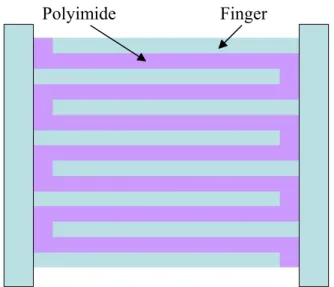
Figure 1-1 shows the structure of the humidity sensor [7][8][9]. The humidity sensor consists of comb electrodes, a comb polysilicon heater and the polyimide. There is a capacitor between the adjacent two fingers. The insulator inserted into the gap between the adjacent two fingers is polyimide. Polyimide is a kind of capacitive sensitive material. The dielectric constant of polyimide varies with the relative humidity in the air. The sensing principle of the humidity sensor is based on the phenomenon of electrical permitivity change of a humidity sensitive film due to absorption and desorption of water vapor.
The humidity sensor was fabricated with TSMC 1P6M 0.18um CMOS process. The deposition of the thin film made of polyimide needs some post-processing steps. The minimum distance between two adjacent fingers is 2 μm. The overlap of adjacent two fingers is 350 μm. The total number of the finger is 100. The total capacitance of the humidity sensor is 3 pF, and the change capacitance of the sensor varies from 0 to 300 fF.
Figure 1-1 Structure of capacitive humidity sensor
1.3 Thesis
Organization
This thesis is organized into five chapters. In Chapter 1, this thesis and the humidity sensor architecture are briefly introduced. In Chapter 2, the basic concepts of quantizer and quantization noise, and fundamentals of the first-order and second-order sigma-delta modulator are introduced. The non-linear effects of the sigma-delta modulator and design of analog circuits are also introduced. Finally, the performance of sigma-delta modulator is presented in detail.
In Chapter 3, the analysis of the proposed sigma-delta modulator used for capacitive sensors is done by MATLAB simulation. First, the analysis of the first-order sigma-delta modulator is presented. Then, the analysis of the second-order sigma-delta modulator is discussed and the parameters of the second-order system are determined by MATLAB.
In Chapter 4, an ultra low power sigma-delta modulator using amplifier operating in weak inversion is introduced. All transistors of the amplifier operating in weak inversion can greatly reduce the power consumption. However, it leads to a large chip area. Some other techniques used in low-voltage low-power sigma-delta modulator are presented.
In Chapter 5, the conclusions of this work are summarized. All the simulation result are also summarized in this chapter..
Chapter 2
Fundamentals of
Sigma-Delta Modulator
2.1 Introduction
Some of the fundamental issues in the design of sigma-delta modulators will be reviewed in this chapter. The first-order sigma-delta modulator is presented in Section 2.2. It includes the basic analysis of the quantization noise, the z-domain linear model, and nonlinear effects due to finite gain of the amplifier. In Section 2.3, we introduce the second-order sigma-delta modulator. The z-domain linear model, nonlinear effects, and alternative structures are introduced. In Section 2.4, some practical design considerations of sigma-delta modulator are taken into account.
2.2
First-order sigma-delta modulator
2.2.1 Quantization
noise
A 1-bit quantizer is the heart of all single quantizer sigma-delta modulators. The analysis of the behavior of a sigma-delta modulator must include the behavior of the
quantizer. Since the quantizer is a nonlinear element, the analysis is complicated even in a simple system. Before the analysis, we modeling the quantizer as the linear model shown in Figure 2-1. The signal e(n) is the adding quantization error, which is the difference between input and output signals. The linear model becomes approximate as long as the quantization error, e(n), is an independent white-noise signal[1].
Figure 2-1 Quantizer and its linear model
At the beginning, the quantization error, e(n), is assumed to be an independent random number with uniform distribution. The signal e(n) uniformly distribute between ± ∆ 2, where ∆ is the difference between two adjacent quantization levels. Figure 2-2 is the power spectral density of quantization noise, e(n).
Figure 2-2 Power spectral density of quantization noise
Assume the total noise power is ∆2 12 and fs is the sampling frequency. With a two-sided definition of power, the area under Se
( )
f within2
s
f
± is equal to the total noise power, or mathematically,
( )
2 2 2 2 2 2 - 2 - 2 12 s s s s f f e x x s f S f df f k df k f ∆ = = =∫
∫
(2.1)Solving equation (2.1), k equals x 1
12 fs ∆ ⎛ ⎞ ⎜ ⎟ ⎝ ⎠ [1]. e(n) y(n) x(n) y(n) x(n) e(n)=y(n)-x(n)
( )
e S f 2 s f 0 -2 s f 1 Height 12 x s k f ∆ ⎛ ⎞ = = ⎜ ⎟ ⎝ ⎠ f2.2.2
Linear model of first-order sigma-delta modulator
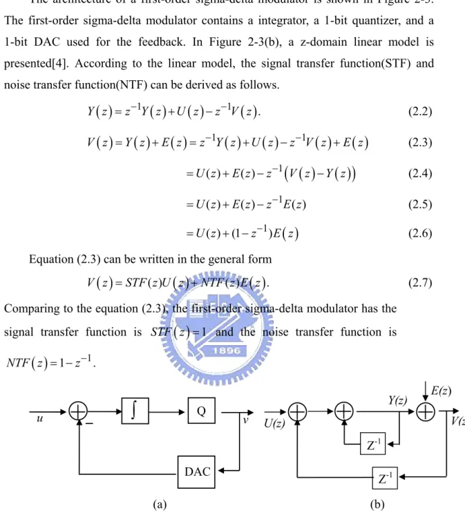
The architecture of a first-order sigma-delta modulator is shown in Figure 2-3. The first-order sigma-delta modulator contains a integrator, a 1-bit quantizer, and a 1-bit DAC used for the feedback. In Figure 2-3(b), a z-domain linear model is presented[4]. According to the linear model, the signal transfer function(STF) and noise transfer function(NTF) can be derived as follows.
( )
1( )
( )
1( )
. Y z =z Y z− +U z −z V z− (2.2)( )
( )
( )
1( )
( )
1( )
( )
V z =Y z +E z =z Y z− +U z −z V z− +E z (2.3)( ) ( )
(
)
1 ( ) ( ) U z E z z− V z Y z = + − − (2.4) 1 ( ) ( ) ( ) U z E z z E z− = + − (2.5)( )
1 ( ) (1 ) U z z− E z = + − (2.6)Equation (2.3) can be written in the general form
( )
( )( )
( )( )
.V z =STF z U z +NTF z E z (2.7) Comparing to the equation (2.3), the first-order sigma-delta modulator has the signal transfer function is STF z
( )
=1 and the noise transfer function is( )
1 1NTF z = −z− .
(a) (b)
Figure 2-3 (a) Topology of 1st-order sigma-delta modulator, (b) z-domain linear model Let z e= j Tω =ej2π f fs, the noise transfer function can be written as
( )
1 2 2 2 sin 2 s s s s s j f f j f f j f f j f f j f f s e e NTF f e j e j f j e f π π π π π π − − − − − = − = × × ⎛ ⎞ = ⎜ ⎟× × ⎝ ⎠ (2.8)Take the magnitude of the noise transfer function, we have Q
∫
DAC U(z) Y(z) Z-1 Z-1 u v V(z) E(z)( )
2sin s f NTF f f π ⎛ ⎞ = ⎜ ⎟ ⎝ ⎠ (2.9)Assume the signal bandwidth of the system is fB, we define the oversampling ratio, OSR, as 2 s B f OSR f ≡ . (2.10)
Based on the above assumption, the quantization noise power over the frequency band from 0 to fB is given by
( )
( )
2 2 2 2 1 2sin 12 B B B B f f e f e f s s f P S f NTF f df df f f π − − ⎛∆ ⎞ ⎡ ⎛ ⎞⎤ = = ⎜⎜ ⎟⎟ ⎢ ⎜ ⎟⎥ ⎝ ⎠ ⎣ ⎦ ⎝ ⎠∫
∫
(2.11)Recalling that the quantization noise power is assumed to be ∆2 12. When fB<< f , we can approximate s sin
(
( )
π f fs)
to be( )
π f fs . The equation (2.7) can be calculated as3 2 2 1 36 e P OSR π ∆ ⎛ ⎞ = ⎜ ⎟ ⎝ ⎠ (2.12)
And the maximum signal power 2
2
s M
P = , where M is the peak amplitude of the full-scale sin wave. Hence, the in-band signal-to-quantization-noise ratio(SQNR) is approximately
(
)
3 2 2 2 36 2 s e M OSR P SQNR P π = = ∆ (2.13)From equation (2.9), it shows that the SQNR increases by 9 dB for each doubling of the OSR[4].
2.2.3
Stability and nonlinear effects
Since the first-order sigma-delta modulator contains only one pole, the system guarantees an unconditionally stability. However, this prediction doesn’t consider the actual signal processing performance in the circuit. In time-domain analysis, the designer should take into account the nonlinearities. Consider the stability when the loop is under DC excitation. If the input is larger than the feedback, the loop will become unstable and output is not bounded.
The analysis in Section 2.2.2 is under an ideal condition. Here, we discuss an non-ideal case with finite gain. Figure 2-4 shows a simple parasitic insensitive integrator. Assume the amplifier in Figure 2-4 has an finite gain A . Then the difference equation which applies to the charge conservation on integrator capacitor
2
C is
( )
( )
( )
( )
(
)
(
)
1 in 1Vout n 2 out Vout n 2 out 1 Vout n 1
C V n C C V n C V n A A A − ⎡ ⎤ ⎡ ⎤ − = ⎢ − ⎥− ⎢ − − ⎥ ⎣ ⎦ ⎣ ⎦(2.14) For C1 =C2 and A>> , 1
( )
1 1 2 1 1 1 1 out in V C z V C z A − = ⎛ ⎞ − −⎜ ⎟ ⎝ ⎠ (2.15)The pole of the integrator is slightly less than 1. The integrator is therefore lossy or leaky. If A OSR> , the additional noise is less than 0.2dB. Hence, the nonlinear effect is not serious. A more important thing is to make sure that the amplifier gain is linear.
Figure 2-4 Switch-capacitor integrator
2.3 Second-order
sigma-delta
modulator
2.3.1
Linear model of second-order sigma-delta modulator
In the previous section, we introduce the fundamentals of the first-order sigma-delta modulator. However, the first-order sigma-delta modulator in terms of resolution and idle-tone generation is not suitable for most applications. In this section, we focus on the second-order sigma-delta modulator. Figure 2-5 shows the z- domain linear model of the second-order sigma-delta modulator.
C1 C2 Vin ψ1 ψ1 ψ2 ψ2 Vout E(z)
Figure 2-5 Linear model of 2nd-order sigma-delta modulator
From the figure,
( )
( )
( )
(
( )
)
( )
(
)
( )
(
)
( )
( )
(
)
1 1 1 1 2 1 1 1 1 2 1 1 1 1 1 1 1 1 V z E z z V z z V z U z z z z E z z z z V z U z z − − − − − − − − − ⎡ ⎤ = + ⎢− + − + ⎥ − ⎣ − ⎦ ⎡ ⎤ − −⎢ − + ⎥ + ⎣ ⎦ = − (2.16)From equation (2.12), it follows that
( )
( )
(
1 1)
2( )
V z =U z + −z− E z (2.17)
Hence, the signal transfer function is STF z
( )
=1, and the noise transfer function is( )
(
1 1)
2NTF z = −z− . Comparing the noise transfer function with first-order
modulator, we know that there is an increased attenuation of quantization noise at low frequencies. The magnitude of the noise transfer function is given by
( )
2 2 2sin s f NTF f f π ⎛ ⎛ ⎞⎞ = ⎜⎜ ⎜ ⎟⎟⎟ ⎝ ⎠ ⎝ ⎠ , for OSR>>1. (2.18)Calculate the total quantization noise power over the band of interest, we obtain 5 2 4 1 60 e P OSR π ∆ ⎛ ⎞ ≅ ⎜ ⎟ ⎝ ⎠ (2.19)
The maximum signal power 2
2
s M
P = , where M is the peak amplitude of the full-scale sin wave. And the maximum in band signal-to-quantization-noise ratio(SQNR) is given by 1 1 1 − − z 1 1 1 − − z 1 −
z
+ − − V(z) U(z)(
)
5 2 2 4 60 2 M OSR SQNR π = ∆ (2.20)We can see from equation (2.16) that doubling the OSR improves the SQNR for a second-order sigma-delta modulator by 15 dB.
2.3.2 Nonlinear
effects
The dynamic behavior of the second-order sigma-delta modulator with a 1-bit quantizer is more complex than those of the first-order sigma-delta modulator. From the analysis in [5], we realize that the quantizer’s gain is in fact signal-dependent. Figure 2-6 shows an example of the quantizer transfer curve(QTC) to illustrate the nonlinear effect of the second-order sigma-delta modulator. The quantizer is based on the cubic approximation, 3
1 3
v k y k y= + . We can use this model to estimate the harmonic distortion induced by the signal-dependent quantizer’s gain.
Figure 2-6 An empirical-determined quantizer transfer curve
For a small low-frequency sin-wave which has amplitude A , the local average of the output follows the input, and thus the local average of the quantizer input is also a low-frequency sin-wave which has an amplitude of A k1. The amplitude of the third harmonic induced by the QTC is k A k3
(
1)
3 4. The third harmonic distortion is(
)
2 3 3 3 1 1 , 4 k A HD NTF z k k = , (2.21)where NTF z k
(
, 1)
is the effective noise transfer function with quantizer gain k1. When the input is large, the distortion is severe.2.3.3
Alternative second-order sigma-delta modulator
1 -1 0 1 -1 ideal cubic
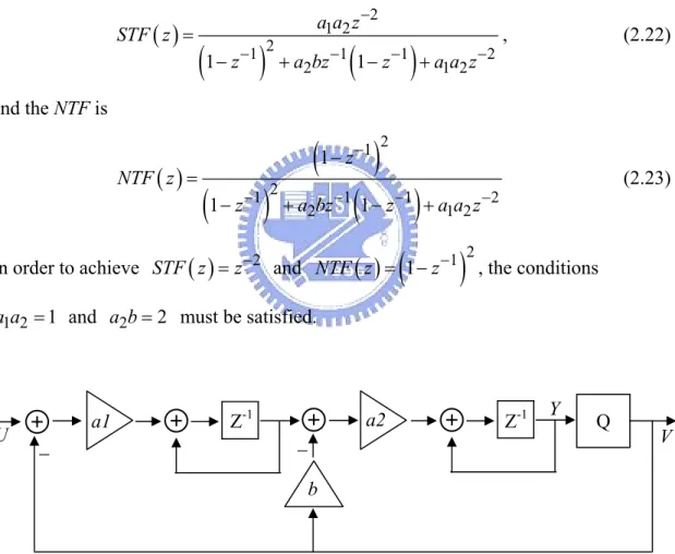
Several alternative structures are available to perform a second-order sigma-delta modulator. In design these structures, the designer should take care to avoid delay-free loops and do a robust design against the unavoidable non-ideal effects such as finite amplifier gain, mismatch of the passive component, etc. Here, we introduce the Boser-Wooley modulator[25], the Silva-Steensgaard structure, and the Error-Feedback structure.
The first one which we will introduce is the Boser-Wooley modulator shown in Figure 2-7. The structure contains two delaying integrators. The using of the delaying integrator allows the amplifier to settle independently of each other. According to the linear analysis, the STF is
( )
(
)
(
)
2 1 2 2 1 1 1 2 2 1 2 1 1 a a z STF z z a bz z a a z − − − − − = − + − + , (2.22) and the NTF is( )
(
)
(
)
(
)
2 1 2 1 1 1 2 2 1 2 1 1 1 z NTF z z a bz z a a z − − − − − − = − + − + (2.23)In order to achieve STF z
( )
=z−2 and NTF z( )
= −(
1 z−1)
2, the conditions 1 2 1a a = and a b2 =2 must be satisfied.
Figure 2-7 The Boser-Wooley modulator
Second, we will introduce the Silva-Steensgaard structure shown in Figure 2-8. The features of this circuit are the direct feedforward path from the input to the quantizer and the single feedback path. According to the linear analysis, the STF and NTF is proofed to be the same as before. The structure has a significant advantage that the loop filter does not need to process the signal and reduces the requirement of
a1 a2 b Q Z-1 Z-1 Y − − U V
linearity.
Figure 2-8 Silva-Steensgaard structure
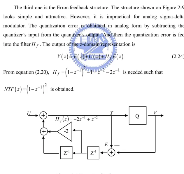
The third one is the Error-feedback structure. The structure shown on Figure 2-9 looks simple and attractive. However, it is impractical for analog sigma-delta modulator. The quantization error is obtained in analog form by subtracting the quantizer’s input from the quantizer’s output. And then the quantization error is fed into the filterHf . The output of the z-domain representation is
( )
( )
( )
f( )
V z =E z +U z +H E z (2.24) From equation (2.20), Hf = −
(
1 z−1)
2 − =1 z−2 −2z−1 is needed such that( )
(
1 1)
2NTF z = −z− is obtained.
Figure 2-9 Error-Feedback structure
Z-1 Z-1 1 1 2 Q Y V Z-1 Z-1 Q -2 Y E
( )
z =−2z−1 +z−2 Hf U U V2.4
Considerations of analog circuit design for
sigma-delta modulators
2.4.1 Introduction
Both the fundamentals of the first-order and second-order sigma-delta modulators have been introduced in the preceding two sections. Now, we are concerned on the practical design considerations. In the Section 2.4.2, we discuss the architectural design concepts. In the Section 2.4.3, the non-idealities at the circuit level are taken into account. In the last section, the analog components that affect the performance of the system are presented.
2.4.2
Architectural design considerations
The architectures of the sigma-delta modulators can be divided into two categories: single-stage modulators and cascaded modulators. Single-stage modulators such as those presented in Sections 2.2 and 2.3 are more tolerant of circuit non-idealities than the cascaded ones. In the thesis, we adopt the single-stage architecture in our design for the following reasons.
1. Single-stage modulators are more tolerant on gain errors that result from capacitor mismatch in switched-capacitor integrators.
2. Single-stage modulators are also tolerant of the integrator leakage that results from the finite DC gain of amplifier.
3. The single-stage modulators are simple and suitable for the design of low power modulators.
Another issue is how to choose an appropriate OSR for the modulator. The use of a higher OSR generally increases the unit-gain bandwidth and slew rate of the amplifier. A higher OSR also have larger power consumption. However, a larger OSR can reduce the chip area of the modulator by the reduction of the sampling and load capacitors. The choice of the OSR is a trade off between power consumption and chip area.
2.4.3
Circuit level non-idealities
non-idealities at their inputs. As a result, operational amplifiers with a large DC gain and capacitors with a low voltage-coefficient is required to implement the first integrator. The integrator transfer function will differ from the ideal one due to the nonzero switch resistance, finite bandwidth, and finite gain. These non-ideal transfer functions are given separately. For finite gain A,
( ) (
)
(
(
)
)
(
)
(
)
1 1 2 1 2 1 1 2 1 1 1 1 C C z A C AC H z C AC z − − − − = − − (2.25)For finite amplifier bandwidth, B(in hertz),
( )
(
)
(
)
(
)
1 1 1 2 2 1 2 1 1 1 C C z z C C C H z z ε ε − − − ⎡ − + + ⎤ ⎣ ⎦ = − , S BT e π ε = − (2.26)For nonzero switch resistance, R , on
( ) (
1 2)
1 / 4 1 1 (1 2 ) 1 s on T R C C C z e H z z − − − − = − (2.27)From equations (2.21), (2.22), and (2.23), we know that finite amplifier gain and incomplete linear settling cause gain error. Fortunately, the gain error has little effect on the performance of a single-loop modulator. The other non-idealities are the voltage-dependent capacitors, signal-dependent switch charge injection, and nonlinear amplifier DC transfer function.
In order to eliminate the distortion of the sigma-delta modulator, the designer should take into account all the non-idealities discussed above. The best way to deal with the non-idealities is to have a good quantitative understanding of these causes and effects.
2.4.4
Modulator component design considerations
A feedback DAC and a comparator are the two important components in the closed-loop modulator. In this section, we will introduce these two component and their design considerations.
The DAC controls the mapping between the analog and digital domains. Hence, the accuracy of the feedback DAC influences the performance of the sigma-delta modulator. There are three non-idealities caused by 1-bit DACs used in sigma-delta modulators:
and the reference voltage. Time-domain multiplication results in a convolution in the frequency-domain. Therefore, signals on the reference with spectral components near the sticks of the output bit stream will cause these sticks to be modulated and convolved. The sticks will be transferred down to the frequencies near DC, known as idle tones.
2. Charge-taking non-idealities: the instant when the amount of charge is delivered to the integrator by the DAC must be identical for the clock cycle. If it is not, it will cause unwanted signals on the reference.
3. Charge-delivery non-idealities: if the charge stored on the feedback capacitor in the DAC is not fully delivered to the integrator each clock cycle, a gain error can occur.
Next, we will consider the design of the comparator. The non-idealities of the comparator can be reduced by the noise-shaping function of the loop. But there are still some design issues for the designer to take into account. The most important one is the metastability of the comparator. Another issue should be concerned is the hysteresis of the comparator. Hysteresis in the comparator makes the present output depending on the previous output. On the other hand, the comparator has memory on it’s output. This memory can create unwanted system poles that may causes errors in the signal and noise transfer functions.
2.5 Summary
The sampling rate of Nyquist A/D converters is only twice of the signal band. However, it is difficult to achieve high resolution A/D conversion due to requirements of accurate anti-aliasing filters. The oversampling technique is a good approach to achieve high resolution A/D converters. The sigma-delta modulator is the most used architecture in the oversampling A/D converters. For the area of sensors, a low power high resolution A/D converter is necessary. The sigma-delta modulators which combined with the front-end circuits for sensors are preferred because it can reduce the power consumption. In order to achieve a higher resolution, the non-linear effects due to the imperfection of the circuits should be taken into account. Another important issue is the tonal behavior which can degrade the SNR should also be taken into consideration. Some practical solutions that can reduce the non-linear phenomenon described in the previous sections should be added into the circuit-level
Chapter 3
The Proposed
Low-Voltage Low-Power
Sigma-Delta Modulator
for Humidity Sensors
3.1 Introduction
In this chapter, the structure of the proposed sigma-delta modulator is presented. We introduce the proposed first-order sigma-delta modulator for humidity sensors in Section 3.2. In Section 3.3, the proposed second-order sigma-delta modulator is introduced. The oversampling ratio and the effect of finite-gain amplifier are simulated by MATLAB. In Section 3.4, the tonal behavior of both first-order and second-order sigma-delta modulators are discussed. The methods to reduce the tonal behavior are also presented.
3.2
The First-Order Sigma-Delta Modulator
3.2.1 Circuit
Architecture
sensors[16][17][18]. Based on the sigma-delta technique, the first-order sigma-delta modulator detects the capacitance change and provides the digital readout with good accuracy. The structure consists of a SC integrator, a comparator, and a simple 1-bit feedback DAC.
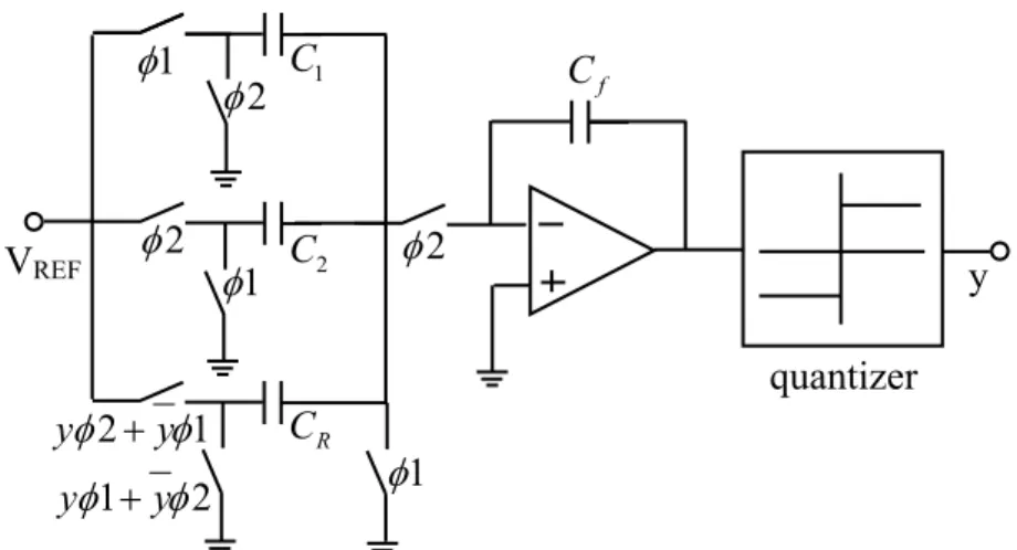
Figure 3-1 The first-order sigma-delta modulator
In the proposed circuit, C1 is the sensor capacitor, C2 is the reference capacitor, and CR is used for the feedback DAC.The basic idea of the proposed sigma-delta modulator is based on the two types of parasitic insensitive integrators shown in Figure 3-2. The parasitic insensitive integrator is a critical component in high-accuracy switched-capacitor integrated circuits. The first one shown in Figure 3-2(a) is a noninverting SC integrator. The transfer function is found to be
( )
( )
( )
1 1 1 2 1 out in V z C z H z V z C z − − ⎛ ⎞ = = ⎜ ⎟ − ⎝ ⎠ (3.1)The second one shown in Figure 3-2(b) is a delay-free integrator. It has the transfer function as
( )
( )
( )
1 1 2 1 1 out in V z C H z V z C z− ⎛ ⎞ = = −⎜ ⎟ − ⎝ ⎠ (3.2)By combining the two types of SC integrators[2][3], we can implement a front-end circuit which can detect the capacitance difference of the sensor. So in our design, a capacitance-to-voltage converter is not needed. The power consumption in our design is reduced comparing to other approaches.
quantizer 1 φ 1 φ 1 φ 2 φ 2 φ φ2 f C 1 C 2 C R C 2 1 φ φ y y + 1 2 φ φ y y + y VREF
(a)
(b)
Figure 3-2 (a) Noninverting SC integrator (b) Delay-free SC integrator
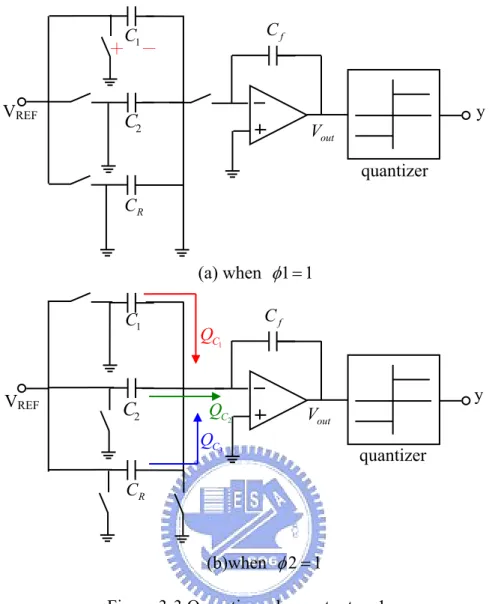
In order to understand the operation of the proposed circuit, how the circuit works at each phase is shown in Figure 3-3 and 3-4. Figure 3-3 illustrates the operation when output y=1 at each phase. Figure 3-4 illustrates the operation when output y=0 at each phase.
1
φ
φ
1 2φ
2φ
1 CC
2 Vout 1φ
1φ
2φ
2φ
1 CC
2 Vout Vin VinFigure 3-3 Operation when output y=1
At phase 2φ , total charge transferring into integrator capacitor Cf causes
( )
1 REF 2 REF R REFout f C V C V C V V n C − − = (3.3)
From the same mechanism when y=0 as shown in Figure 3-4, the output voltage of the integrator is given by
( )
1 REF 2 REF R REFout f C V C V C V V n C − + = (3.4)
Assume K1+K2 =K, K1 is the number of the cycles when y=1, and K2 is the number of the cycles when y=0. Combine both equations (3.3) and (3.4)and base on the concept of the sigma-delta technique, we obtain the relation between input and
f C quantizer quantizer f C 2 C 1 C 2 C 1 C R C R C out V out V + - (a) when 1 1φ = (b)when 2 1φ = VREF VREF 1 C Q 2 C Q 3 C Q y y
output as follows:
1 2 1 2
1 REF REF R REF 2 REF REF R REF 0
f f C V C V C V C V C V C V K K C C − − + − + =
(
K1 K2)(
C1 C2)
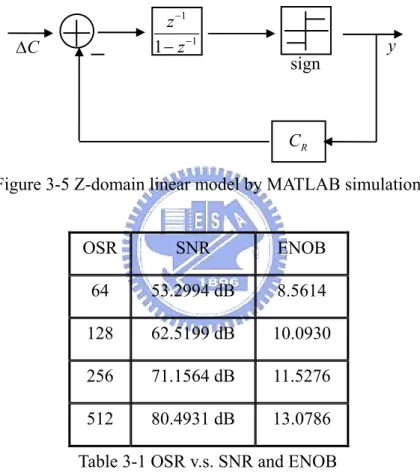
K C1 R K C2 R 0 ⇒ + − − − = 1 2 1 2 avg R C K K y C K K ∆ − ⇒ = = + (3.5)Figure 3-4 Operation when y=0
From equation (3.5) derived above, ∆C is the difference between sensor capacitor and reference capacitor. After K clock cycles, the circuit provides digital output according to the capacitance change.
3.2.2
Determine OSR and finite gain of the operational amplifier
As discussed in Section 2.4.2, choosing an appropriate OSR is important in the quantizer quantizer VREF VREF f C f C 1 C 1 C 2 C 2 C R C R C y y out V out V 1 C Q 2 C Q 3 C Q (a) when 1 1φ = (b)when 2 1φ =
design of sigma-delta modulator. In this section, our goal is to determine an OSR for the system to achieve 10-bit resolution. The analysis is done by the MATLAB simulation based on the z-domain linear model. We construct the system in SIMULINK as shown in Figure 3-5. By changing different OSR of the simulated system, we obtain the result in Table 3-1. Table 3-1 shows the relationship between OSR and peak SNR. We know that doubling OSR increases peak SNR approximately by 9dB. The outcome is the same as shown in section 2.2.2. According to Table 3-1, we choose OSR >128 to meet our requirement.
Figure 3-5 Z-domain linear model by MATLAB simulation
OSR SNR ENOB
64 53.2994 dB 8.5614 128 62.5199 dB 10.0930 256 71.1564 dB 11.5276 512 80.4931 dB 13.0786 Table 3-1 OSR v.s. SNR and ENOB
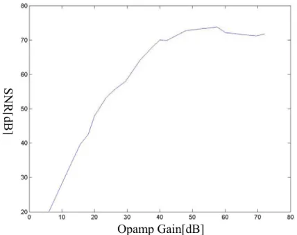
By replacing the ideal integrator by a leaky integrator due to the finite gain of the amplifier, we analyze the effect of leaky integrator and obtain the minimum requirement of the DC gain of the amplifier. We choose OSR to be 256 in this analysis. The simulation result from SIMULINK is shown in Figure 3-6. It shows the obtained SNR versus the amplifier gains in the proposed structure. The minimum gain requirement for amplifier is 40dB to ensure over 70dB SNR of the first-order modulator. The gain requirement is only determined by the noise shaping consideration. If the distortion of the circuit should be taken into consideration, a higher amplifier gain should be achieved to ensure a better distortion performance.
1 1 1 z z − − − R C sign C ∆ y
Figure 3-6 SNR versus amplifier gain
3.2.3 SNR
Prediction
In this section, we derive the mathematical equation to predict the SNR accurately. The derivation utilizes the linear model shown in Figure 3-7. The model includes the integrator leakage. This means that the factor β is less than 1. ∆Cis the capacitance change of the sensor, E is the quantization noise, and Y is the output of the modulator.
Figure 3-7 Linear model of the proposed structure
The signal transfer function is found to be
( )
(
)
1 1 1 1 1 1 1 1 R R Y C C z C = βz− z− = β z− ∆ − + − − . (3.6) Z-1 Z-1( )
Y z( )
E z( )
C z ∆ β − − Opamp Gain[dB] SNR [dB ]The noise transfer function is given by
( )
(
)
1 1 1 1 1 1 1 1 1 1 Y z z E z z z β β β − − − − − = = − − + − . (3.7)Assume ∆C is a sinusoidal input with peak amplitude M , the signal power can be calculated as
(
)
(
)
2 2 2 1 0.5 1 1 2 1 R s M C P β β ⎛ ⎞ × ×⎜ ⎟ ⎝ ⎠ = + − − − (3.8)The quantization noise power is calculated as
( )
(
)
(
)
2 2 2 2 1 1 2 sin 2 2 2 e P E z OSR OSR β β π β β ⎡ + ⎛ ⎞⎤ ⎢ ⎥ = × − ⎜ ⎟ ⎢ − − ⎝ ⎠⎥ ⎣ ⎦ (3.9)By equation (3.8) and (3.9), peak SNR of the first-order modulator is given by
( )
(
)
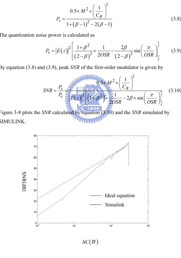
2 2 2 2 1 0.5 1 1 2 sin 2 R s e M C P SNR P E z OSR OSR π β β ⎛ ⎞ × ×⎜ ⎟ ⎝ ⎠ = = ⎡ + × − × ⎛ ⎞⎤ ⎜ ⎟ ⎢ ⎝ ⎠⎥ ⎣ ⎦ (3.10)Figure 3-8 plots the SNR calculated by equation (3.10) and the SNR simulated by SIMULINK.
( )
∆C fF SNR [dB ] Ideal equation SimulinkFigure 3-8 SNR versus input amplitude
The simulation results in Figure 3-8 show that the SNR of the first-order system degrades heavily. Since the results from the ideal equation do not include harmonics, the SNR decreases due to idle tones. This shows that the quantization noise is not white when the input is small.
3.3 The
Second-Order
Sigma-Delta
Modulator
3.3.1 Circuit
Architecture
In this section, a second-order sigma-delta modulator is introduced. A higher order structure can cancel the pattern noise of the first-order sigma-delta modulator and reduce the measurement time. Figure 3-9 shows the proposed second-order sigma-delta modulator. The second-order modulator is obtained by including a second stage which has the transfer function[17]
( )
4 3 4 2 2 1 2 1 1 f z C C C z K H z K C z z − − ⎛ ⎞ ⎛ ⎞ = − ⎜ ⎟= − ⎜ ⎟ − ⎝ − ⎠ ⎝ ⎠ . (3.11)Figure 3-9 Proposed second-order sigma-delta modulator
In order to determine the coefficients of the second stage, we do the performance simulation by SIMULINK. The block diagram constructed in SIMULINK is shown in Figure 3-10. At the beginning of the simulation, we set the coefficient K1 to be 1 and OSR to be 64. This is because the output of the second stage is connected to the quantizer. The gain of the second stage is not the key factor that affects the overall performance of the modulator. Table 3-2 shows the simulated result with coefficient
2 f C 1 f C 1 C 2 C R C 3 C 4 C 1 φ 2 φ 1 φ 1 φ 1 φ 1 φ 1 φ φ2 φ2 2 φ 2 φ 1 2 yφ +yφ 2 1 yφ +yφ quantizer 2 φ y
( )
2 H z VREF2
K varying from 0.1 to 0.9. According to table 3-2, the coefficient K2 is set to be 0.6 to achieve the best performance of the modulator. The other coefficient K1 will be adjusted according to the need of the circuit implementation.
Figure 3-10 Z-domain linear model by MATLAB simulation
2
K 0.1 0.2 0.3 0.4 0.5 0.6 0.7 0.8 0.9
SNR[dB] 46.05 52.55 59.84 65.17 69.91 70.16 69.41 66.57 60.57 Table 3-2 Coefficient K2 versus SNR
3.3.2
Determine OSR and finite gain of the operational amplifier
The same step as in Section 3.2.2 is to choose an appropriate OSR for the second-order sigma-delta modulator. Our goal is to determine an OSR for the system to achieve 10-bit resolution. The analysis is done by the MATLAB simulation based on the z-domain linear model. We consider only the quantization noise shaping. By varying the different values of OSR of the system, the result in Table 3-3 is obtained. We know that doubling OSR increases the peak SNR approximately by 15dB from Table 3-3. According to the simulation results, we choose OSR to be 64 to have 10-bit resolution. OSR SNR ENOB 16 41.3482 dB 6.5761 32 55.7793 dB 8.9733 64 70.1610 dB 11.3623 128 83.7637 dB 13.6219 Table 3-3 OSR versus SNR and ENOB
1 1 1 z z − − − 1 2 1 1 1 1 K z K z − − − − − R C sign C ∆ y
Another important parameter we have to decide is the DC gain of the operational amplifier used in the modulator. We use the same way to analyze the minimum gain requirement of the amplifier. All ideal integrators are replaced by leakage integrators in our analysis. The OSR is set to be 64 for our analysis. Figure 3-11 shows the obtained SNR versus the gain. The minimum gain requirement is 30dB to ensure an peak SNR over 70dB.
Figure 3-11 SNR versus amplifier gain
3.3.3 SNR
Prediction
The SNR versus input amplitude is plotted in Figure 3-12. The curve is obtained by SIMULINK. The full-scale of the input is from 0 to 300 fento Farad, and the feedback capacitor CR is set to be 300 fento Farad. The peak SNR is measured approximately 71dB. When the input amplitude is large, the overload of the quantizer greatly degrades the SNR. Figure 3-13 shows the power spectrum of the second-order sigma-delta modulator when input amplitude is 200 fF.
Amplifier Gain[dB]
SNR
[dB
Figure 3-12 SNR versus input amplitude
Figure 3-13 Power spectrum
3.4 Tonal
Behavior
3.4.1
Tonal behavior of first-order sigma-delta modulator
It is well understood that first-order sigma-delta modulators produces tones. In our analysis in SIMULINK, we obtain the three power spectrums shown in Figure
SNR
[dB
]
( )
3-14, 3-15, and 3-16. We know that idle tones becomes large when the input is small. This kind of idle tone is input-dependent. This is because when the input amplitude is small, the quantization noise power spectrum is not white. The only way to solve this problem is to utilize a higher-order sigma-delta modulator. There are many factors that affecting the tonal behavior includes DC input level, initial condition of the loop filter, finite amplifier gain, and switch charge injection. In order to eliminate the tonal behavior, we should take all these parameters into considerations in our design.
Figure 3-14 When the input amplitude is 200fF
Figure 3-16 When the input amplitude is 10fF
3.4.2
Tonal behavior of second-order sigma-delta modulator
As the analysis in first-order sigma-delta modulator, we obtain the power spectrum of different input amplitude in Figure 3-17, 3-18, and 3-19. The three figures shows that when the input becomes large, the overload effect of the comparator is obvious. The quantization noise is not white when the input amplitude is large, so the harmonic tones degrades the performance of the second-order sigma-delta drastically. In our practical design, the phenomenon should be taken into considerations.
Figure 3-18 Input amplitude is 250fF
Figure 3-19 Input amplitude is 300fF
3.4.3
Methods for tone decorrelation
In this section, we discuss the methods for tone decorrelation. The methods are introduced as follows [5]:
1. Dithering: this method increases the noise floor but reduce the power of the harmonic tones.
2. Chaos: moving one or more noise transfer function zeros outside the unit circles. 3. Adding an out-of-band sine or square wave: it is typically common to use a
frequency that is a submultiple of the oversampling clock.
4. Adding a DC offset to the input of the modulator: this pushes the idle channel noise spectral to higher frequencies outside the baseband.
5. Adding a small amount of random noise to the input: the small inherent thermal noise in an analog implementation will suffice as an appropriate dither.
6. Using analog sources of noise within the modulator: this technique has the potential of producing a result similar to that of noise-shape dither, but only if the
noise magnitude is sufficient and predictable in the actual hardware implementation.
7. Using high-order modulators: the quantization noise becomes white when the higher modulator is used.
All the methods described above are used to randomize the quantization noise. As long as the quantization noise is not white, the tonal behavior becomes obvious and degrades the SNR heavily. As the simulation results shown in section 3.4, the tonal behavior is more serious in the first-order modulator than in the second-order one. The second-order modulator is adopted in our design in order to reduce the idle tones.
3.5 Summary
There are many system parameters which need to be determined in sigma-delta modulator, such as OSR, sampling clock, and DC gain of the amplifier. In Section 3.2, the oversampling ratio is determined to be 256, and DC gain of the amplifier should be larger than 40dB for the first-order sigma-delta modulator to achieve over 10-bit resolution. The OSR is set to be 64 for the second-order sigma-delta modulator, and the DC gain of the amplifier should be larger than 30 dB. By comparing the first-order and second-order modulators, the second-order modulator will consume less power than the first-order one due to the decrease of OSR. From Section 3.4, it shows that the tonal behavior of first-order sigma-delta modulator is more obvious than the second-order one. According to the analysis done by MATLAB, we decide to implement the second-order sigma-delta modulator proposed in section 3.3. The low voltage techniques for the design of the sigma-delta modulator will be introduced in Chapter 4.
Chapter 4
A 1.5
µ
W Switched-Capacitor
Sigma-Delta Modulator For
Humidity Sensors
4.1 Introduction
In this chapter, the second-order sigma-delta modulator is implemented with low voltage low power techniques described in the following sections. We develop a design flow which is suitable for the design of the amplifier operating in weak inversion in Section 4.2. In Section 4.3, the basic blocks used for the modulator is presented, including a bias circuit, amplifier, and integrators. The design of a 1-bit quantizer is discussed in section 4.4. The structure of the non-overlapping clock generator is shown in section 4.5.
4.2
Circuits Design in Weak Inversion
In the past thirty years, the characteristics of MOS operating in weak inversion have been studied by many authors. It is well known that when the gate-to-source voltage of a MOS transistor is reduced below the threshold voltage defined in the strong inversion, the channel current decreases exponentially. There are many demands for the design of low power analog integrated circuits in recent years, such as pacemakers, hearing aids, and neural networks. In our system, the humidity sensor is used to detect the humidity in the living environment. So a long life time of battery is needed in our sensor system. The system presented in Chapter 3 is designed in weak inversion. A very simple model which is suitable for circuit design is discussed in next section.
Figure 4-1 Operating region of a MOS transistor
4.2.2
Simple Model in Weak Inversion
The simple model discussed in this section is based on the following assumptions[10].
1. The channel is sufficient long so that gradual channel approximation can be used and channel-length modulation is negligible.
2. Generation currents in the drain, channel, and source depletion regions are negligible; source and drain currents are then equal.
3. The density of fast surface states and the fluctuations of surface potential are negligible.
The equation of the drain current in weak inversion are derived as
weak inversion moderate inversion strong inversion GS th V −V 20mV 80 200mV− D I
/ ( ( / ) / )
th T G T S T D T
V nU V nU V U V U
D S
I =SI e− e e− −e− (4.1)
S is the aspect ratio, W
L . Is is the characteristic current
2
2n Uβ T . For 0VBS = and VDS >4UT, equation (4.1) can be simplified as
(VGS Vth) /nUT D S I =SI e − (4.2) , where 1 d ox C n C = + is usually between 1.5~1.6.
The upper limit of the drain current in weak inversion is
2
ID 2nKWUT L
< (4.3)
From equation (4.2), the transconductance, gm, of MOS transistor in weak inversion is given by D D m G T I I g V nU ∂ = = ∂ (4.4)
The channel length modulation effect is essentially the same for MOS transistors in weak inversion and strong inversion. The output resistance, rds, is given by
1 ds D r I λ
= , λ is the channel length modulation factor (4.5)
4.2.3
Design Flow of Low Power Operational Amplifiers
In order to simplify the design of operational amplifier operating in weak inversion, we must develop a useful design flow to determine the small-signal parameters given in the previous section. The design methodology we proposed in this section is based on gm ID method [14]. The methodology is suitable for the design of CMOS analog circuits operating in all regions of operation. It is especially suited for the design of low power analog circuits operating in weak inversion because it provides a good compromise between speed and power consumption. The gm ID method is chosen for the following three reasons.
1. It is strongly related to the performance of analog circuits. 2. It gives an indication of the device operating region.
3. It provides a tool for calculating the transistors dimensions.
design of operational amplifiers, the two parameters, transconductance and slew rate, are taken into considerations first. The transconductance of the input differential pair is obtained according to the requirement of unit-gain bandwidth. The output current is determined by the slew rate and output loading. According to the relation of gm ID and ID
(
W L)
, we can determine the aspect ratio of each transistor with obtained transconductance and DC current. After choosing the aspect ratio of each transistor, take them into HSPICE simulation. Adjust the aspect ratio iteratively and make sure all the requirements are satisfied. Figure 4-3 is the plot of gm ID versus(
)
D
I W L of n-MOS transistors, and Figure 4-4 is for p-MOS transistors.
Figure 4-2 Design flow
D
I W L
Set DC bias point for suitable ICMR and output swing.
Start D L I SR C = D I 2 2 D nW T I nK U L <
Are all requirements satisfied? m T g =ω C yes no Finish D m T I g nU = (minimum size) W L v.s. m D D g I I W L W L m D g I
Figure 4-3 gm ID versus ID
(
W L)
of NMOSD
I W L
Figure 4-4 gm ID versus ID
(
W L)
of PMOS4.3
Implementation of Integrators
4.3.1 Low
Voltage
Low
Power Operational Amplifier
The amplifier is the main building block of the sigma-delta modulator. It determines the total power consumption of the modulator. According to the comparison in [21], a single-stage amplifier is more power efficient than two-stage amplifier. So the current-mirror amplifier proposed in [21] is preferred, and all transistors are operated in weak inversion to meet the ultra low power requirement. The minimum gain requirement for the amplifier is 40dB to ensure 10-bit resolution from Section 3.3.2. The architecture of the current mirror amplifier is shown in Figure 4-5. The B factor is the current gain from the diode-connected transistor to the transistor connected to the output node. Transistors M3a and M4a are added to enhance the DC gain without extra power consumption. The unit-gain bandwidth of the proposed topology is derived as
1 2 m L B g UGB C π ⋅ = , where m D T I g nU = in weak inversion. (4.6) The above equation shows that unit-gain bandwidth will be multiplied by B. The DC gain of the current mirror amplifier is obtain by
(
11 3)
m o dc g r B A k ⋅ ⋅ = − . (4.7)The parameter k is between 0 and 1, and k should be appropriately determined to
m D
g I
maintain a safe phase margin. In our design, the current mirror amplifier has DC gain of 60dB and unit-gain bandwidth of 68 kHz. The simulation result in different corner is shown in Figure 4-6.
Figure 4-5 Proposed low power operational amplifier
Figure 4-6 Frequency response in different cases
4.3.2
Bias Circuit in Weak Inversion
The disadvantage of analog blocks operating in weak inversion is the high sensitivity to temperature variation. In order to reduce the effect of temperature variation, the bias circuit shown in Figure 4-7 generates a constant current, IREF,
irrelative to temperature. The bias circuit is composed of a PTAT current source and a VEB referenced current source. The PTAT current source, I1, is formed by transistors
M1, M2, M3, M4, and R1.The PTAT current source, I1, is given by
4 1 1 1 3 2 ln T nV S S I R S S ⎛ ⎞ = ⎜ × ⎟ ⎝ ⎠. (4.8)
The VEB referenced current source is formed by M5, M6, M7, M8, Q1, and R2. The
M3a M4a M0 M1 M2 1: B M3 M4 kI in1 in2 out V Gain [dB] Phase [degree]
current source I2 is given by 2 2 EB V I R = . (4.9)
Since the temperature coefficient of I1 is positive, and the temperature coefficient of 2
I is negative, the reference current, IREF , can be temperature independent by appropriately adjusting K1 and K2. The bias circuit consumes less power than many other bias circuits used for analog circuits operating in weak inversion. In our design, all transistors are operating in weak inversion, and the transistor Q1 is the lateral BJT. Many bias circuits, such as in [13] and [15], are designed in strong inversion which consumes more power. The simulation result in Figure 4-8 shows that the maximum reference current variation is 6nA when temperature varies from 0 to 100.
Figure 4-7 Bias circuit
M1 M2 M3 M4 R1 M5 M6 M7 M8 2 R 1 Q M9 M10 M11 1 1 K I 2 2 K I 1 I 2 I REF I 6nA
Figure 4-8 IREF versus Temperature
4.3.3 Switch
Consideration
In switch-capacitor circuits, a MOS switch is a most often used components. The MOS switch nonidealities includes a nonzero and nonlinear on-resistance, clock feedthrough, channel charge injection, sampled noise, and leakage current. We consider clock feedthrough and channel-charge injection. The two factors may produce idle tones in sigma-delta modulators. When the switch is turned off, the channel charges are released and removed through MOS source and drain terminal. The charges inject into the integrating capacitor and affect the accuracy of the integrator.
The simplest way to reduce the effect of the charge injection is to use complementary switches. However, the technique is inefficient due to the mismatch of the n-MOS and p-MOS devices. The matching between the channel charges of the n-MOS and p-MOS devices is poor and signal dependent. In our design, we adopt the n-MOS switch with two compensating dummy switches, M2 and M3, shown in Figure 4-9[20]. In order to force the channel charges to flow equally into the source and drain terminal, clock phases with short transition time is used. The size of dummy switches is set to be half of the switch M1.
Figure 4-9 Switch with dummy
4.3.4 Voltage
Multiplier
In order to guarantee an adequately low switch resistance in a low voltage switched-capacitor circuits, the output voltage of the clock used to drive the switches can be boost higher than supply voltage. Therefore, the voltage multiplier technique is implemented. It doubles the output voltage of each clock phase. Figure 4-10 shows a voltage boosted clock driver used in our design. C1 and C2 are charged to Vdd via the
cross-coupled NMOS M1 and M2. When the input clock, CK, goes high, the output voltage, CKsw, is boosted to 2Vdd. However, the output can not actually reach 2Vdd
φ
φ φ
M1