國立交通大學
材料科學與工程學系
碩士論文
結合高介電質材料與三五族半導體之金氧半電容研究
Study of High-k/III-V MOS Capacitors
研 究 生:宋先敏
指導教授:張 翼 博士
Study of High-k/III-V MOS Capacitors
研 究 生:宋先敏 Student: Hsien-Ming Sung
指導教授:張 翼 博士 Advisor: Dr. Edward Yi Chang
國立交通大學
材料科學與工程學系
碩士論文
A Thesis
Submitted to Department of Materials Science and Engineering
College of Engineering
National Chiao Tung University
in partial Fulfillment of the Requirements
for the Degree of
Master of Science
in
Materials Science and Engineering
August 2009
Hsinchu, Taiwan, Republic of China
結合高介電質材料與三五族半導體之金氧半
電容研究
研究生:宋先敏 指導教授: 張 翼 博士
國立交通大學材料科學與工程學系
摘要
互補式金氧半場效電晶體之發展將在到達 22 奈米結點時遇到瓶頸,結合高介電 質材料與高電子遷移率三五族半導體的研究逐漸受到重視。由於有著極佳的載子 傳導特性,三五族金氧半場效電晶體將會是未來高頻低操作偏壓應用的選擇。然 而高介電質材料與三五族半導體的介面問題始終阻礙著三五族金氧半元件的發 展。隨著薄膜沉積技術的進步,原子層沉積法以及分子束磊晶技術已經能夠成長 高品質的介電材料於三五族半導體上研究金氧半電容的特性。 本論文主要利用分子束磊晶機台成長二氧化鉿,氧化鐠和氧化鈰來製作金氧半電 容並研究其特性。我們在二氧化鉿與砷化銦鎵的電容上得到了等效氧化層厚度為 2.9 奈米的良好尺寸微縮特性,並在具有高銦含量的電容上發現了載子反轉的行 為。 我們同時也研究了具有相當高介電常數的氧化鐠以及氧化鈰的電容特性,並發現 若以氧化鐠取代二氧化鉿將可得到較高的聚集電容值。費米能帶釘扎的問題也在 元件退火溫度的研究中得到解決。 氧化鐠與氧化鈰組成的層狀結構的電容特性也同時被研究。我們發現針對層狀結 構所作的二步驟退火將可以增加元件的聚集電容值,其原因我們將利用穿透式電 子顯微鏡的圖片來說明。Study of High‐k/III‐V MOS Capacitors
Student: Hsien‐Ming Sung Advisor: Dr. Edward Yi Chang
Department of Materials Science and Engineering
National Chiao Tung University
Abstract
Due to its superior carrier transport capability, III-V based MOS field effect transistor technology has the potential of being used for future high frequency low power application. However, the lack of high quality native oxides has been the obstacle for years. Thanks to high-k dielectric deposition technology improvement, high quality gate dielectrics can now be deposited on III-V material for MOS capacitor studies, which is very important before fabricating III-V MOSFETs.
In this thesis, molecular beam epitaxy (MBE) was used to deposit HfO2, Pr6O11, and
CeO2 for MOS capacitors study. Good scalability was obtained with equivalent oxide
thickness (EOT) equal to 2.9nm on HfO2/InxGa1-xAs/InP MOS capacitors. The
inversion behavior was also observed for high indium concentration InxGa1-xAs, the
mechanism is discussed in this thesis.
Pr6O11 and CeO2, which have very high dielectric constant, were also deposited on
InxGa1-xAs for MOS capacitor study. It was found that after replacing HfO2 with
Pr6O11, the accumulation capacitance increases owing to the high dielectric constant
of Pr6O11. The annealing temperature was characterized to unpin the surface Fermi
level.
The CeO2/ Pr6O11 gate stack structure was also studied; two step annealing was
introduced to improve the accumulation capacitance. The reason of the capacitance increase was also observed by cross-sectional TEM image.
誌謝
兩年的碩士生活一轉眼便過去,在這之中經歷了許許多多的事情,每件都令我如 數家珍並且心懷感激。首先感謝老師在我當初找指導教授四處碰壁時願意讓我加 入複合物半導體實驗室,可以說沒有老師便沒有今天的回憶更無法認識我所珍惜 的大家,每每看到老師獨自留在辦公室處理事情到深夜都令我對老師工作的態度 感到尊敬,實驗室也因老師的帶領才有今天的茁壯。其次是帶我的林岳欽學長, 跟在學長身邊的兩年我學到了不只是技術,更多的是做人處事的道理,後者將會 是我未來數十年在社會上打滾時所奉行的金科玉律,如果沒有這兩年的磨練或許 我在社會上可能會走得更跌跌撞撞。在材料分析上我要感謝延儀學長和宏偉學長 的幫忙,深夜的歐傑分析有兩位陪伴都不會孤單。我同時也要謝謝我第一個合作 的外國朋友 Dang,真的很謝謝你與我討論分析數據,每次都能有很多心得。再 來是我寶貝的同學老皮、阿伯、黑妞、小麥、阿K和蘇煜翔,一同打拼的兩年是 無法磨滅的復刻回憶,尤其是老皮跟阿伯,謝謝你們在我剛進入交大這個陌生環 境時主動找我聊天介紹你們的同學給我認識,讓我結交了不少朋友。最後是與我 朝夕相處的 409 的大家,不論是以前的鴨王、小丸子、小禮和大琦還是現在的宏 偉、珍珍、鼎鈞、柏菁和俊佑,能夠和你們同一間研究室是我最大的幸運,與你 們天馬行空不著邊際的談天是支持我每天進出無塵室的動力,每次想起都讓我莞 爾一笑,也謝謝你們在逼著聽我抱怨時還願意給我安慰與鼓勵。我想跟你們每個 人都說一句話表達我的感謝。給宏偉:希望你一切的努力都有收穫能讓你早點畢 業,不要被實驗上的挫折打敗,你是我看過最厲害的人。給珍珍:偷偷跟妳說, 我當初第一眼看到妳的時候就想要是妳能坐 409 就真的太好了,每次看到妳都覺 得很愉快忍不住就會笑出來,妳真的有散播快樂的能力。給柏菁:你超認真的但 還是不要讓自己壓力太大,有這麼正的女朋友夫復何求咧,謝謝你常常很晚還陪 我吃宵夜,朋友就是降當的。給鼎鈞:說真的,有時你不聽話我超怒的,但當我 觀察到你對你所專注的事情都能做得很好以及能堅持自己的意見時,我反而變得非常的羨慕,希望你能在你的事業上有所成就,開公司時記得照顧學長一下。給 俊佑:雖然我常常說你長得壞壞的但其實我是想跟你說我覺得你看起來超酷的, 腿又長又會跳舞講話又好笑讓我超級忌妒的。 最後的最後,我要謝謝親愛的爸爸、媽媽還有阿姨從小對我無微不至的照顧,讓 我不需要考慮課業之外其他的事情順利的拿到碩士學位,將來請讓我來照顧你 們。
Contents
ABSTRACT (CHINESE)
I
ABSTRACT (ENGLISH)
II
ACKNOWLEDGMENTS
III
CONTENTS
V
TABLE CAPTIONS
VII
FIGURE CAPTIONS
VIII
CHAPTER 1
INTRODUCTION
1
1.1
Research motivation
1
1.2
Challenges for high‐k/III‐V MOS devices
1
CHAPTER 2
METAL-OXIDE-SEMICONDUCTOR CAPACITORS
5
2.1
Basic structure and principle of operation
5
2.2
Differential MOS capacitance
8
2.3
Non‐ideal MOS capacitor
9
2.3.1 Interface traps and oxide charges 10CHAPTER 3
HIGH-K/III-V MOS CAPACITORS REVIEW
17
3.1
Criteria for choosing high‐k dielectrics
17
3.2
Device characterization
18
3.2.2 Conductance measurement 19 3.2.3 Extract Dit from conductance method 20
CHAPTER 4
EXPERIMENTAL
25
4.1
Device structures
25
4.2
Process flow
25
4.2.1 Wafer cleaning 25 4.2.2 Surface treatment 25 4.2.3 High‐k dielectric deposition 26 4.2.4 Electrodes metal formation 26CHAPTER 5
RESULTS AND DISCUSSION
28
5.1
Study of HfO
2/ In
xGa
1‐xAs MOS capacitors
28
5.2
Capacitance increase by replacing Pr
6O
11to HfO
2as gate oxide on
In
xGa
1‐xAs
30
5.3
Capacitance increase by using two‐step annealing process on
CeO
2/Pr
6O
11gate stack structure
32
CHAPTER 6
CONCLUSION
49
REFERENCE
51
Table Captions
Table 3‐1 Comparison of relevant properties for high‐K candidates [18] 22
Table 5‐1 Extracted equivalent oxide thickness (EOT) from 10kHz curve of
CeO2/Pr6O11/InAs devices 48
Table 5‐2 Extracted equivalent oxide thickness (EOT) from 10kHz curve of HfO2
Figure Captions
Fig. 1-1 ITRS roadmap of CMOS scaling 4
Fig. 1-2 Drift velocities vs. electrical field as a parameter of semiconductors 4
Fig. 2-1 Basic Metal-oxide-semiconductor capacitor structure 11
Fig. 2-2 Energy band diagram of an ideal MOS capacitor at V=0 11
Fig. 2-3 Energy band diagram of an ideal MOS capacitor in accumulation 12
Fig. 2-4 Energy band diagram of an ideal MOS capacitor in depletion 12
Fig. 2-5 Energy band diagram of an ideal MOS capacitor in inversion 13
Fig. 2-6 Energy band diagrams at the surface of a p-type semiconductor 13
Fig. 2-7 Cross section of an MOS capacitor showing a simple equivalent circuit of
oxide capacitance COX and semiconductor capacitance CD in series 14
Fig. 2-8 Schematic low- and high-frequency C-V curves showing accumulation,
depletion and inversion 1 4
Fig. 2-9 (a) Energy band diagram of an isolated metal and an isolated semiconductor with an oxide layer between them. (b) Energy band diagram of an MOS
capacitor in thermal equilibrium 1 5
Fig. 2-10 Schematic charges distribution of thermally oxidized silicon 15
Fig. 2-11 Effect of a fixed oxide charge and interface traps on the C-V characteristics
of an MOS capacitor 16
Fig. 3-1 Schematic band offsets of high-k dielectrics on GaAs [19] 22
Fig. 3-3 Schematic Fermi level pinning phenomenon [20] 23 Fig. 3-4 Schematic experimental and modeled interface state conductance [21] 24 Fig. 3-5 Equivalent circuits for conductance measurement: (a) MOS-C with interface trap time constant τit=RitCit, (b) simplified circuits of (a), (c) measured circuit, (d)
including series rs resistance and tunnel conductance Gt[22] 2 4
Fig.4-1 Structures of MOS capacitor in this study 2 7
Fig. 4-2 Process flow of High-k/III-V MOS capacitor fabrication 2 7
Fig. 5-1 C-V curves of (a) 12nm, (b) 9nm and (c) 6nm HfO2 on In0.53Ga0.47As PDA at
600OC 34
Fig. 5-2 C-V curves of HfO2 (9nm)/InAs devices. (a) PDA at 500OC. (b) PDA at
400OC 35
Fig. 5-3 (a)-(b) Equivalent circuits including interface trap effects, Cit and Rit. (c) Low
frequency case. (d) High frequency case [28]. 36
Fig.5-4 Interface trap densities for (a) 500OC (b) 400OC annealed devices 37
Fig. 5‐5 Hysteresis of HfO2 (9nm)/InAs devices. 37
Fig. 5-6 Comparison of C-V characteristics between (a) 9nm Pr6O11 and (b) 9nm
HfO2 on In0.7Ga0.3As 38
Fig. 5-7 C-V curves of Pr6O11 (10nm)/In0.53Ga0.47As devices (a) PDA at 450OC. (b)
PDA at 500OC (c) PDA at 550 OC. The hysteresis of 1MHz curves of two
samples are shown in the inset figure. 4 0
Fig. 5-8 TEM image of 550OC annealed Pr6O11/In0.53Ga0.47As device 4 1
Fig. 5-9 (a) C-V curve, (b) TEM image and EDX analysis of CeO2(9nm)/In0.7Ga0.3As
device. 42
Fig. 5-11 Comparison of C-V characteristic between (a) one-step annealing process (only Pr6O11 was annealed at 500OC), and (b) two-step annealing process
(Pr6O11 was first annealed at 500OC, second step annealing was performed
at 400OCafter CeO2 deposition) for CeO2 (8nm)/Pr6O11 (4nm)/InAs devices
44
Fig. 5-12 TEM images of (a) one-step annealed and (b) two-step annealed CeO2
(8nm)/Pr6O11(4nm)/InAs devices. 4 5
Fig. 5-13 C-V curves of CeO2(6nm)/Pr6O11(4nm)/InAs devices of different annealing
temperatures. (a) Pr6O11 was first annealed at 500OC, followed by 400OC
annealing after CeO2 deposition. (b) Pr6O11 was first annealed at 550OC,
followed by 400OC annealing after CeO2deposition. 4 6
Fig. 5-14 TEM images of CeO2(6nm)/Pr6O11(4nm)/InAs devices first step annealed at
(a) 500OC (b) 550OC. And both annealed at 400OC after 6nm CeO2
deposition. The Pr6O11 beneath the CeO2 transform from amorphous type to
Chapter 1
Introduction
1.1 Research motivation
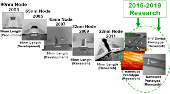
Moore’s Law predicts that the numbers of transistors on an integrated circuit will double every two years. In order to continue this trend, the size of the transistors must be minimized. Strained-Si channel with SiGe buffer layer was used to increase the channel mobility and hence improve the device performance [1-2]. But when the
device size was further scaled down to 45nm node, the SiO2 was too thin to prevent
direct tunneling. High-k dielectric has since been introduced as an alternative gate oxide. However consumer product’s urgent need of high performance device have forced the transistor size further scaling down to its limit. According to the ITRS roadmap for semiconductor (Figure 1-1), silicon is expected to scale to 22 nm. III-V semiconductor material has been researched actively as alternative channel material to silicon for complementary metal-oxide-semiconductor (CMOS) applications at the 22 nm technology node and beyond due to its intrinsic superior transport property.
1.2 Challenges for highk/IIIV MOS devices
To meet the demands of ITRS roadmap and follow Moore’s law, various solutions like high-k dielectrics and high mobility channels including stained-Si, germanium and III-V materials have been researched rigorously. Silicon technology is predicted to reach its limit when entering 22nm node, germanium and III-V material are expected to be alterative p- and n-type channel material for high speed application due to their superior transport properties than silicon as shown in figure 1-2. For III-V materials, characteristics like direct band gap and band engineering have been used in
optoelectronic and high frequency applications. How to integrate III-V material with high-k dielectrics is the challenge to be dealt with now.
The main challenge for integrating high-k on III-Vs is the interface issue. Unlike silicon, the lack of high quality native oxide has been the main obstacle for decades, limiting the implementation of logical and digital applications. Great number of interface traps in the forbidden gap pin the Fermi level, causing so called Fermi level pinning phenomenon, which makes devices unworkable [3]. Many efforts have been done to solve this problem, including anodic treatment, thermal and plasma oxidation of III-V semiconductor surface, but all failed to give electrically and thermodynamically stable gate insulator with low interface traps.
In the past few years, sulfide and ammonia pretreatments were proved to effectively reduce the native oxide and passivate the semiconductor surface. With advanced deposition technology, high quality gate oxide like MBE grown Ga2O3(Gd2O3) [4], or
ALD grown Al2O3 [5-8] and HfO2 [9-12] with low interface trap density of
~1011eV-1cm-2 could be achieved. In this study, MBE was used to deposit HfO2,
Pr6O11, and CeO2 on high indium concentration InxGa1-xAs for MOS capacitors.
HfO2, owing to its good thermal stability, high dielectric constant and also high
energy band gap, it is widely studied on silicon as well as III-V semiconductors. Pr6O11 was used in this study due to it provides high dielectric constant of 32 and
similar energy band gap as HfO2. As for the CeO2, the energy band gap of CeO2 is
very low, only 3.2eV, and exhibits very diffusive characteristic when directly depositing on InGaAs. But its relatively high dielectric constant of 52 [13] and single crystalline structure inspired us to integrate it with InGaAs by applying gate stack structure.
Most MOS capacitor studies on InxGa1-xAs semiconductor substrate were related to
concentration. In this thesis, various high-k/ InxGa1-xAs configured MOS capacitors
Fig. 1-1 ITRS roadmap of CMOS scaling
Chapter 2
Metal-Oxide-Semiconductor Capacitors
The primary reason to study Metal-Oxide-Semiconductor capacitor (MOSCAP) is to understand the principle operation as well as the detailed analysis of the Metal-Oxide-Semiconductor Field Effect Transistor (MOSFET). The MOSCAP is very important in semiconductor device because it is very useful in the study of semiconductor interface. In practical application, it is the kernel of MOSFET, which is the most important device in integrated circuits. It also can be used as a storage capacitor in integrated circuits. In this chapter, the basic MOS structure and its four different modes of operation namely accumulation, depletion, inversion and flatband are studied.2.1 Basic structure and principle of operation
The MOS capacitor structure is illustrated in figure 2-1. On the top is the gate metal followed by a thin oxide layer; below the thin oxide layer are the semiconductor substrate and the back side metal forming an Ohmic contact.
According to different doping types in substrates, MOS capacitors can be categorized into two types: NMOS with p-type substrate and PMOS with n-type substrate due to inversion layer contains electrons in p-type substrate and holes in n-type substrate. Following discussions are all using p-type substrate based MOS capacitor.
Figure 2-2 is the band diagram of an ideal MOS. Where q m and q s stand for work function of metal and semiconductor respectively, which is the energy difference between the Fermi level and vacuum level. And qX is the electron affinity, the energy difference between the conduction band and the vacuum level in semiconductor. Eg is
Fermi level EF and intrinsic Fermi level Ei. The ideal MOS is defined as: (a) at zero
bias, the work function difference between metal and semiconductor q ms is zero.
q q m q s q m qX E qψB 0 (1)
In other words, the energy band is flat when there is no applied voltage, thus, figure 2-2 is also referred as flatband condition. (b) The only charges that exist in the capacitor under any biasing conditions are those in the semiconductor and those with equal but opposite sign on the metal surface adjacent to the oxide.(c) There are no carrier transport through the oxide under any direct current biasing conditions, on the other hand, the resistivity of oxide is infinite [17].
For ideal MOS capacitor, when one applies positive or negative voltage, the capacitor will be operated in three cases. For instance, when a negative voltage is applied to the NMOS, the excess positive carriers (holes) will accumulate at the oxide-semiconductor interface. In this condition, the band near the interface is bent upward as shown in figure 2-3. The upward bending of intrinsic Fermi level Ei at the
interface will increase the energy difference Ei-EF, which in turn give rise to an
enhanced hole concentration. This is called accumulation condition.
When small positive voltage is applied, the energy band is bent downward, as shown in figure 2-4, the majority carriers will be depleted, and the capacitor is now operating in depletion condition.
As an even larger positive voltage is applied, the energy band bent even more, the intrinsic Fermi level at interface is now crossing over the Fermi level, as shown in figure 2-5. In this case, the interface between oxide and semiconductor is like n-type semiconductor, which means, the positive voltage starts to induce electrons at the interface. In this case, the amount of minority carrier (electron) is greater than majority carrier (hole), the interface is thus inverted, an inversion layer is formed, and
the capacitor is in inversion condition.
In the beginning, the electron concentration is larger than ni but still smaller than
substrate doping concentration NA, the capacitor is in weak inversion. Once the
electron concentration in inversion layer reaches NA, the condition strong inversion
will occur.
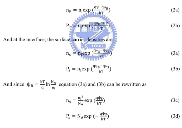
Figure 2-6 shows the energy band diagram at the interface of oxide and p-type semiconductor. The electrostatic potential ψ is defined as zero in the bulk of the semiconductor and positive when the band is bent downward, where ψs is the surface potential, by using this concept, the electron density and hole density can be written as a function of ψ:
nP n exp ψ TψB (2a)
PP n exp ψBT ψ (2b)
And at the interface, the surface carrier densities are:
n n exp ψS ψB
T (3a)
P n exp ψB ψS
T (3b)
And since ψB TlnNA equation (3a) and (3b) can be rewritten as
n N Aexp S T (3c) P NAexp S T (3d)
The above discussions of flat-band, accumulation, depletion and inversion are summarized below:
ψS 0 Accumulation of holes (bands bend upward) ψS 0 Flat-band condition
ψS ψB Midgap with ns=np=ni (intrinsic condition)
ψS ψB Inversion (bands bend downward)
2.2 Differential MOS capacitance
The behavior of small-signal capacitance variation with gate bias of MOS capacitor can provide further understanding of the electrical behavior of the MOS system. The
static MOS capacitance is defined as C QV , where Q is the total charge on the
capacitor and V is the gate bias. The small-signal differential capacitance per unit area is: C QS VG (4) For VG VOX ψS with VOX QS OXA QS OX, equation (4) becomes: C QS OX QS S OX S QS COX CD (5)
where CD’ stands for semiconductor capacitance per unit area or depletion-layer
capacitance per unit area. Equation (5) also implies that the total capacitance of the MOS capacitor is the series of the fixed capacitance of the oxide and the variable capacitance of the semiconductor as shown in figure 2-7, which depends on the applied gate voltage through the ΨS.
When the MOS capacitor is in depletion mode, equation (5) can be rewritten as C
COX S W
(6)
Once the depletion region width reaches its maximum (VG=VT), the capacitance has it
minimum value, the capacitance per unit area at maximum depletion becomes: C
OX W
S
(MOS capacitance at maximum depletion) (7)
When the capacitor is in accumulation mode, depletion region diminishes. The capacitance has its maximum value which is equal to COX’.
C
OX COX
COX (MOS capacitance in accumulation) (8)
When the applied voltage VG>VT, there are two extreme conditions: at low frequency,
the electron in inversion layer can follow the AC small-signal, the capacitance of the inversion region is equal to the accumulation capacitance, the minority carriers are in thermal equilibrium with the small-signal; and if the frequency is high enough that the minority carriers can not follow, the capacitance will remain unchanged from its value at VG=VT, which is the minimum capacitance of the maximum depletion.
The capacitance per unit area of depletion, accumulation and inversion of high and low frequency are shown in figure 2-8.
2.3 Nonideal MOS capacitor
The discussions in former chapters were all assumed that the capacitor is ideal. For non-ideal MOS capacitor there are work function difference, q ms, between gate metal and semiconductor, and also the charge in the oxide need to be considered, which will all change the flat-band voltage of the capacitor.
The work function difference
The work function of a semiconductor q s, which is the energy difference between the vacuum level and the Fermi level, varies with doping concentration. For a given metal with a fixed work function, the work function difference between the metal and
semiconductor is defined as q q q .
Figure.2-9(a) shows the energy band diagram of an isolated metal and an isolated semiconductor with a oxide layer between them. At thermal equilibrium, the Fermi level should be aligned and the vacuum level should be continuous, which results in the band diagram shown in Fig.2-9(b), the band bending is to accommodate the work function difference. When there is work function difference, the flat-band voltage no longer be zero, an additional voltage must be applied to make the energy band flat.
The flat-band voltage difference between non-ideal and ideal capacitor is
∆VFB VFB VFBO . (9)
2.3.1 Interface traps and oxide charges
Except for the work function difference, the MOS capacitor will also be affected by charges in oxide and traps in the oxide-semiconductor interface. The basic classification of these traps and charges are shown in Fig.2-10. They are interface-trapped charge (Qit), fixed-oxide charge (Qf), oxide-trapped charge (Qot) and
mobile ionic charge (Qm).
With considering ms, Qf,Qot, and Qm, the flat‐band voltage shift becomes
∆VFB VFB VFBO Q QCO Q (10)
The C-V curves of ideal and non-ideal MOS capacitor are shown in Fig.2-11 (a) and (b), respectively. The presence of ms, Qf,Qot, and Qm shift the flat-band voltage by
an amount given by equation (10); if there are large amounts of interface-trapped charges, the interface-trapped charges will vary with surface potential and make the C-V curve stretched-out, which is as shown in Fig.2-11(c).
Fig. 2-1 Basic Metal-oxide-semiconductor capacitor structure
Fig. 2-3 Energy band diagram of an ideal MOS capacitor in accumulation [17]
Fig. Fig. 2-5 Energy ba 2-6 Energy ba and diagram o and diagrams of an ideal MO at the surface OS capacitor i e of a p-type s in inversion [1 emiconductor 17] r [17]
Fig. 2-7 Cross section of an MOS capacitor showing a simple equivalent circuit of oxide capacitance COX and semiconductor capacitance CD in series [17]
Fig. 2-8 Schematic low- and high-frequency C-V curves showing accumulation, depletion and inversion
Fig. 2-9 (a) Energy band diagram of an isolated metal and an isolated semiconductor with an oxide layer between them. (b) Energy band diagram of an MOS capacitor in thermal equilibrium [17]
Fig. 2-11 Effect of a fixed oxide charge and interface traps on the C-V characteristics of an MOS capacitor [17]
Chapter 3
High-k/III-V MOS Capacitors Review
3.1 Criteria for choosing highk dielectrics
1. Dielectric constant and barrier height:
When choosing the gate dielectrics, usually the dielectric constant is the number of thumbs we will consider. But as the thickness is decreasing, preventing direct tunneling is also the main function of gate dielectric. Thus the energy band gap and the barrier height are becoming more important. Table 3-1 lists the dielectric constants and energy band gap of commonly used high-k candidates [18] and figure 3-1 and figure3-2 show the calculated band offsets of oxides on GaAs and InAs [19].
2. Thermal stability:
Thermal stability is important due to many MOS process undergo high temperature ambient, including rapid thermal annealing (RTA). To avoid current leakage and sufficiently storage charges, the amorphous type or single crystalline gate dielectrics with high re-crystallization temperature are required.
3. Good interface property:
Interface quality is the most important issue for MOS devices. Carriers at the oxide-semiconductor interface will be trapped if the interface states or traps density (Dit) are too high. For silicon MOS devices, the interface trap density is usually on the
order of 1010eV-1cm-2, but for III-V MOS devices, it was always two or three orders higher than that, which was the main problem for III-V MOS device operation and the origin of Fermi level pinning. Figure 3-3 shows the schematic diagram for Fermi level pinning phenomenon [20]. The high density of interface traps will pin the Fermi level, capture and emit carriers at the interface, which make the device unworkable or result in frequency dispersion among C-V curves measured at different frequency. With the
surface pretreatment before deposition, the native oxide of III-V materials which was considered to be the origin of interface traps and with lower-k value could be reduced. Also with the progress of vacuum technology and new methods for depositing high-k dielectrics, like Atomic Layer Deposition (ALD) and Molecular Beam Epitaxy (MBE), the inversion type III-V MOSFET has been fabricated, but the device performance still need to improve.
3.2 Device characterization
3.2.1 CV measurement
To get the capacitance-voltage characteristic, one can connect the front side and backside electrodes of the device with LCR impedance analyzer probes. By changing the frequency of the supplied AC signal, the high and low frequency CV curves can be plotted. Following are some parameters which are often used to judge the device performance:
1. Equivalent oxide thickness (EOT)
EOT OX S O . It is used to characterize how the given dielectric can achieve the
same capacitance of thin SiO2 layer with thicker physical thickness. 2. Flatband voltage
Flatband voltage is of importance due to it determines the gate voltage at which there are no charge in the semiconductor. It separates the accumulation and depletion conditions. The ideal flatband voltage can be determined by setting the work function difference in the simulation tool and assuming there are no trap charges existing in the oxide or oxide/semiconductor interface. By comparing the flatband capacitance
between the simulated and measured curves, the flatband voltage shift ∆VFB
3. Hysteresis
Hysteresis is measured by sweeping the gate voltage forth and back. The amount of hysteresis stands for the amount of charges trapped by the defects in the oxide, thus it can be used to determine the oxide quality. The clockwise hysteresis implies the negative charges were trapped; on the other hand, the counterclockwise hysteresis implies the positive charges were trapped by the defects. The defects extracted from hysteresis are also called slow trapping states, where the interface traps are fast trapping states.
4. Frequency dispersion
Frequency dispersion is the phenomenon of accumulation capacitance varying with operation frequency. In silicon MOS capacitors, it is due to leakage current of ultra thin oxide, making the capacitor can not storage charge, causing the total capacitance decrease. For high-k/III-V case, the oxide thickness is not as thin as silicon MOS, the causing of frequency dispersion is the poor quality interface where large amounts of interface traps exist at the semiconductor surface. The interface traps are frequency dependent, it will capture and emit charges distorting the C-V curves causing frequency dispersion, and more seriously, will induce Fermi level pinning and stop the device operating.
3.2.2 Conductance measurement
The quality of oxide/semiconductor interface remains essential for MOS device performance. One direct effect moving from traditional Si MOSFET to III-V MOSFET is the high interface state densities (Dit), which are known to strongly affect driving current of the devices.
Some methods have been utilized to evaluate Dit, for example, low frequency method (quasi-static method), high frequency method (Terman method), charge pumping and
conductance method. The first two methods use the capacitance-voltage relationship extracting the Dit, the equivalent components models includes: oxide capacitance, depletion layer capacitance and interface-trap capacitance. Since the depletion-layer capacitance is in parallel with interface trap capacitance, difference in capacitance must be calculated, which leads to inaccuracies in extracting the information of interface state. Further more, although the low frequency quasi-static method was the most common one for dielectrics with low leakage current, but with extremely shrinkage of device size, the leakage current associated with direct tunneling through a thin oxide makes the measurement difficult to perform. Charge pumping is a very sensitive to the interface states but it requires fully processed MOSFET device. In this research, we used conductance method to characterize the interface properties of the MOS capacitors. In chapter 3.2.3, the principle of conductance method of extracting Dit is introduced.
3.2.3 Extract Dit from conductance method
In 1967, Nicollian and Goetzberger of Bell Lab. gave a detailed and comprehensive discussion for the conductance method, in which conductance is directly related to the interface traps, which can give more accurate results. The data extraction is based on the measurement of the equivalent parallel conductance, GP, of a MOS capacitor as a
function of bias voltage and frequency as shown in figure 3-4 [21]. The conductance representing the lossy mechanism from interface trap, capturing and emitting carriers, is an index of the interface trap density. Figure 3-5 shows the equivalent circuit of the measurements [22], where COX, CS, Cit, represent oxide capacitance, semiconductor
capacitance and interface trap capacitance respectively.
The above assumption neglected the series resistance of substrate and oxide leakage
conductance GP is given by equation (1), and Dit is given by equation (2),
GP G COX
G COX C (1)
D . GP (2)
Where (GP/ω)max is the peak value from a GP/ω-frequency plot.
But actually the device does exist series resistance for thin oxide or leaky oxide. The equivalent circuit is converted to figure 3-5(d) with Gt stands for tunnel conductance
and rs stands for series resistance. Equation (1) becomes GP COX G G
G COX C (3)
Where
C G C C G C CG G (4)
The series resistance is determined y biasing the device into accumulation region
r G G C (5)
Cma and Gma are the measured capacitance and conductance in accumulation. The
tunnel conductance Gt is determined from Gc by setting the ω 0
G GG (6)
For rs and Gt equal to 0, equation (3) reverts to equation (1).
Table 3-1 Comparison of relevant properties for high-K candidates [18]
Fig. 3-2 Schematic band offsets of high-k dielectrics on InAs [19]
Fig. 3-4 Schematic experimental and modeled interface state conductance [21]
Fig. 3-5 Equivalent circuits for conductance measurement: (a) MOS-C with interface trap time constant τit=RitCit, (b) simplified circuits of (a), (c) measured circuit, (d) including series rs resistance and tunnel
Chapter 4
Experimental
In this chapter, the structures which were used in this study and the experiment process flow will be described.
4.1 Device structures
The first structure contains 100nm silicon-doped In0.53Ga0.47As layer(n-type,
5x1017cm-3) which was grown on (001) InP substrate by MBE as shown in figure
4-1(a). The second structure contains 5nm In0.7Ga0.3As layer and 10nm In0.53Ga0.47As
layer (both are silicon-doped with doping concentration of 5x1017cm-3) on (001) InP substrate as shown in figure 4-1(b). The third structure contains 5nm InAs layer, 10nm In0.7Ga0.3As layer and 3nm In0.53Ga0.47Aslayer (all are n-type with silicon
doping concentration of 5x1017cm-3) on (001) InP substrate as shown in figure 4-1(c).
4.2 Process flow
4.2.1 Wafer cleaning
The first step is wafer cleaning. The wafers were immersed into ACE and IPA, each for 5 minutes to remove contaminant, and then they were dried by blowing nitrogen gas.
4.2.2 Surface treatment
Surface treatment is a very important step before depositing high-k dielectric on high speed III-V semiconductor. The untreated surfaces are reported to leave native oxide, which will affect the performance. After the treatment, the native oxide is eliminated and a thin passivation film is formed on the top of the semiconductor, which prevents
inner semiconductor react with oxygen in atmosphere.
The (NH4)SX was chosen as surface treatment solution. The dilute HF:H2O (1:100)
solution was first applied for removing the native oxide, followed by dipping the wafer in (NH4)SX for 30 minutes at room temperature. The depth of the passivating
thin film can be determined by the immersing time and reacting temperature.
4.2.3 Highk dielectric deposition
After surface treatment, the wafers were transferred into MBE chamber immediately to prevent them stay too long in atmosphere.
Several high-k dielectrics configuration were chosen to apply on the III-V substrates. Some were deposited singly and some were grown on the other dielectric which was deposited in advance to form composite dielectrics. The rapid thermal annealing (RTA) was held after high-k dielectrics deposition to improve the oxide-semiconductor interface quality, two or only one step RTA process for the composite oxide were also performed to achieve better device characteristics.
4.2.4 Electrodes metal formation
Finally, aluminum was chosen as gate and backside metal, which was deposited by electron gun evaporation.
Fig.4 Fig. 4-1 Structures 4-2 Process fl s of MOS capa flow of High-k
Wafer c
Gate m
forma
Backsid
forma
acitor in this s k/III-V MOS ccleaning
metal
ation
e metal
ation
study capacitor fabrricationSur
treat
Hig
depo
rface
tment
gh‐k
osition
Chapter 5
Results and discussion
5.1 Study of HfO
2/ In
xGa
1xAs MOS capacitors
HfO2 was first deposited on In0.53Ga0.47As with varied thickness of 12nm, 9nm and
6nm for oxide scaling study. Its C-V characteristic is shown in figure 5-1. The equivalent oxide thickness extracted from 10kHz curves were 5.76nm, 3.5nm and 2.9nm, respectively, which showed good scalability. The curves in the negative voltage region exhibited well inversion behavior, which could be referred as unpinning of Fermi level [23]. The deep-depletion phenomenon for devices with 9nm
and 6nm HfO2 can be explained that the minority carriers could not follow the high
frequency small signal, keep biasing the device will further increase the depletion region, resulting in deep-depletion phenomenon [24]. Whether the thickness affects the inversion phenomenon is still under research.
After successfully investigating the HfO2/In0.53Ga0.47As capacitors, HfO2/InAs MOS
capacitors were also studied, the thickness of HfO2 was 9nm. The devices were
annealed under different temperatures to observe the accumulation capacitance change and the inversion behavior. Figure 5-2 shows the C-V characteristic of the
devices which were annealed at 500OC and 400OC. The HfO2/InAs devices didn’t
exhibit deep-depletion as HfO2/In0.53Ga0.47As devices performed. This could be
explained that the minority carrier response time could be shorter in InAs due to its smaller band gap, shorter minority carrier life time (
τL
) and higher intrinsic carrier concentration (1.25x1015cm-3 for InAs, 3.96x1011cm-3 for In0.53Ga0.47As). Furthermore,defects and impurities can also act as source for generation of minority carriers and bulk traps may shorten the minority carrier life time [25]. To fully understand the
minority carrier behavior of device, C-V curves measured at different temperature is still on the progress.
In figure 5-2 (b), device underwent 400OC annealing showed large frequency
dispersion at low frequency as compared to the device underwent 500OC annealing,
which may due to the interface traps’ response. For silicon MOS capacitor, the dispersion phenomenon may due to a very thin and lossy gate dielectric; many models have been constructed to explain this phenomenon [26-27]. But for III-V MOS research, the dispersion phenomenon is mainly due to the interface traps, although mechanism is still not very well understood. Figure 5-3(a) shows the equivalent circuits including interface traps effects. COX and CD are the oxide capacitance and
semiconductor depletion layer capacitance, respectively [28]. Cit and Rit are the
capacitance and resistance associated with the interface traps. They are also the function of energy. The product CitRit is defined as the interface trap life time τit,
which determines its frequency behavior. The parallel branch of figure 5-3 (a) can be
converted into a frequency-dependent capacitance CP and a frequency-dependent
conductance GP in parallel with each other as shown in figure 5-3 (b). CP and GP
which were mentioned in former chapter can also be written as
CP CD C (1)
GP C (2)
At low frequency, Rit can be neglected, and CD is in parallel with Cit. If the
measurement frequency is too high for interface traps to respond, then Cit and Rit can
be ignored. The simplified equivalent circuits for both conditions are shown in figure 5-3 (c) and (d). The measured capacitances for these two conditions are:
CLF CCOX CD C
CHF COXCD
COX CD (4)
For silicon MOS capacitors, when measured at low frequency and biased at the accumulation region, CD is very large due to no depletion region forms, and Cit can be
neglected owing to high quality interface. Thus the total capacitance is equal to COX.
But for III-V case, the capacitance of interface traps must be considered, and is frequency dependent, so that the capacitance is varied with frequency, causing frequency dispersion. Even measured at high frequency, if the frequency is not sufficiently high so that the traps can not response, the frequency dispersion will also be found in high frequency curve. The interface trap distribution for two annealing
temperatures measured at various bias are shown in figure 5-4, 400OC annealed
device exhibited larger interface traps than 500OC annealed device, which could
explain the large frequency dispersion in 400OC annealed C-V curve.
Finally the hysteresis performance of two annealing temperature is shown in figure
5-5. 108mV for 400OC annealed device and 214mV for 500OC annealed device. We
would expect the value could be lower than 100mV after optimizing the annealing temperature.
5.2
Capacitance increase by replacing Pr
6O
11to HfO
2as
gate oxide on In
xGa
1xAs
To investigate the capacitance increasing by replacing Pr6O11 to HfO2 on InGaAs
channel, two type oxides with the same thickness were grown on In0.7Ga0.3As channel.
Figure 5-6 shows the C-V curve of these two devices. The accumulation capacitance was arising apparently in Pr6O11 applied sample. The inversion phenomenon was not
clear, which may due to high interface traps.
Figure 5-7 compares the capacitance-voltage characteristic of Pr6O11
capacitance of 450OC annealed device showed almost no saturation. The transition from accumulation to depletion was not very sharp, indicating poor interface quality. After increasing annealing temperature to 500OC, the transition became conspicuous, and the accumulation capacitance began to saturate, but the inversion behavior still
not very apparent as compared to former device using HfO2, indicating Fermi level
pinning at the oxide/semiconductor interface. The 550OC annealed device showed
inversion behavior, which we speculate that the Fermi level was unpinned. The
deep-depletion phenomenon of 550OC annealed sample could be explained that more
oxide charges (including fix oxide charges and oxide trap charges) were generated during high temperature annealing, which caused large hysteresis as compared to the
500OC annealed device, which is shown in the inset of figure 5-7 (b). The other
possible explanation for the deep-depletion phenomenon in the 550OC device could
be in the microstructure view. Figure 5-8 shows the TEM image of the 550OC
annealed device, the oxide is neither single-crystalline nor amorphous, but poly-crystalline type, which provided leakage current paths for the minority carriers. Since the minority carriers tunnel through the oxide to the gate electrode, the inversion layer could not form [29]. Again, the depletion region will continue to increase to maintain charge balance when keep biasing the device, which resulting in deep-depletion.
From the discussion, we expect that the accumulation capacitance could increase if
single-crystalline of amorphous type Pr6O11 could be grown for better insulation
5.3 Capacitance increase by using twostep annealing
process on CeO
2/Pr
6O
11gate stack structure
Figure 5-9(a) shows the C-V curve of directly deposited CeO2 on In0.7Ga0.3As The
device exhibited no capacitor function, and figure 5-9(b) is the TEM image and EDX analysis of the device. Serious inter-diffusion was found in the device, great amount of indium, gallium and arsenic were detected in the CeO2, which should not occur for
a gate dielectric.
Based on previous study, Pr6O11 was chosen as a diffusion barrier. Figure 5-10 shows
the cross-sectional TEM image and EDX analysis of CeO2 (8nm)/Pr6O11 (6nm)/InAs
device. After applying 4nm Pr6O11 beneath the CeO2 the diffusion was suppressed. The EDX analysis indicated some InGaAs contents still existing in oxide layer, but the device exhibited normal C-V characteristic as shown in figure 5-11.
Figure 5-11 compares the C-V characteristic between two annealing process for CeO2
(8nm)/Pr6O11 (6nm)/InAs device. Both of two devices exhibited inversion behavior,
which we ascribed to the high intrinsic carrier density and short minority carrier response time of low energy band gap InAs layer. The device underwent only
one-step annealing process after Pr6O11 deposition showed lower accumulation
capacitance than that underwent two-step annealing process. Two-step annealing consists of first step annealing at 500OC after Pr6O11 deposition and second step
annealing at 400OC after CeO2 deposition, while one-step annealing only consists of
first step annealing after Pr6O11 deposition. The increase of accumulation capacitance
was owing to the thickness decrease of Pr6O11 after the second step annealing as
shown in figure 5-12, showing the effectiveness of two-step annealing process on those devices with two oxides as gate dielectrics.
To further increase the accumulation capacitance the CeO2 thickness was reduced to
6nm, totally 10nm CeO2/Pr6O11 on InAs. Figure 5-13 compares the C-V
characteristics of two devices with different first step annealing temperature, and both underwent second step annealing at 400OC after CeO2 deposition. For the device first
annealed at 500OC, the capacitance increase was due to the decrease of the CeO2
thickness, but it also accompanied with leakage current increase. The C-V curve of
the device first annealed at 550OC showed more severe current leakage than 500OC
annealed device, which we ascribed to the re-crystallization of Pr6O11 generated
current leakage paths. Figure 5-14 shows the TEM images of the first step 500OC and 550OC annealed devices.
Table 5-1 summarizes the EOT of the CeO2/Pr6O11/InAs devices. As compared to the
HfO2 gated devices shown in Table 5‐2, the CeO2/Pr6O11 gate stack structure showed
large EOT than HfO2, which was not the result we expected. Except for the thickness
for the CeO2/Pr6O11 gate stack were larger than HfO2, the poly‐crystalline structure
and rough surface of the gate stack couldn’t effectively storage the charges which resulted in low accumulation capacitance.
-2 -1 0 1 2 0.4 0.5 0.6 1kHz 10kHz 100kHz 1MHz Cap aci tan ce ( uF /c m 2 ) Gate voltage (V) (a) -2 -1 0 1 2 0.5 0.6 0.7 0.8 0.9 1.0 1kHz 10kHz 100kHz 1MHz Ca pac it a nce ( uF /c m 2) Gate voltage (V) (b) -2 -1 0 1 2 0.6 0.7 0.8 0.9 1.0 1.1 1.2 1.3 1kHz 10kHz 100kHz 1MHz Ca p a ci ta n c e ( uF /c m 2 ) Gate voltage (V) (c)
-2 -1 0 1 2 0.60 0.65 0.70 0.75 0.80 0.85 0.90 0.95 Gate voltage (V) Cap a ci tance ( uF/c m 2 ) 1kHz 10kHz 100kHz 1MHz (a) -2 -1 0 1 2 0.70 0.75 0.80 0.85 0.90 0.95 1.00 1.05 1.10 1.15 Cap a ci tance ( uF/cm 2 ) 1kHz 10kHz 100kHz 1MHz Gate voltage (V) (b)
Fig. 5-3 (a)-(b) Equivalent circuits including interface trap effects, Cit and Rit. (c) Low frequency case.
(d) High frequency case. [28]
-1.0 -0.5 0.0 0.5 1.0 8E11 9E11 1E12 1.1E12 1.2E12 1.3E12 1.4E12 1.5E12 1.6E12 In terfa ce trap d e nsi ty, Dit ( cm -2 eV -1 ) Gate voltage (V)
9nm HfO
2/InAs@500OC
(a)-1.0 -0.5 0.0 0.5 1.0 1.8E12 2E12 2.2E12 2.4E12 2.6E12 2.8E12 3E12 3.2E12 3.4E12 In terfa ce trap d e nsi ty, Di t ( cm -2 eV -1 ) Gate voltage(V)
9nm HfO
2/InAs @400OC
(b)
Fig.5-4 Interface trap densities for (a) 500OC (b) 400OC annealed devices
-2 -1 0 1 2 0.55 0.60 0.65 0.70 0.75 0.80 0.85 0.90 400OC 500OC Capac it ance ( uF /c m 2 ) Gate voltage (V) ΔV=0.108V ΔV=0.214V Fig. 5‐5 Hysteresis of HfO2 (9nm)/InAs devices.
-1.5 -1.0 -0.5 0.0 0.5 1.0 1.5 0.6 0.7 0.8 0.9 1.0 1.1 1.2 1.3 1.4 1kHz 10kHz 100kHz 1MHz Capac it ance ( u F/c m 2 ) Gate voltage(V) (a) -2.0 -1.5 -1.0 -0.5 0.0 0.5 1.0 1.5 0.70 0.75 0.80 0.85 0.90 0.95 1.00 1.05 1kHz 10kHz 100kHz 1MHz Cap a ci ta n ce ( uF/c m 2 ) Gate voltage (V) (b)
-1.5 -1.0 -0.5 0.0 0.5 1.0 1.5 0.7 0.8 0.9 1.0 1.1 1.2 1.3 1.4 1.5 C apa ci ta nc e ( u F/ cm 2 ) Gate voltage (V) 1kHz 10kHz 100kHz 1MHz (a) -1.5 -1.0 -0.5 0.0 0.5 1.0 1.5 0.3 0.4 0.5 0.6 0.7 0.8 0.9 1.0 -2.0 -1.5 -1.0 -0.5 0.0 0.5 1.0 1.5 2.0 0.3 0.4 0.5 0.6 0.7 0.8 1kHz 10kHz 100kHz 1MHz Ca p aci tan ce ( uF/c m 2 ) Gate voltage (V) 500OC 550OC (b)
-1.5 -1.0 -0.5 0.0 0.5 1.0 1.5 0.3 0.4 0.5 0.6 0.7 0.8 0.9 1.0 1kHz 10kHz 100kHz 1MHz Ca p aci tan ce ( uF/c m 2 ) Gate voltage (V) (c)
Fig. 5-7 C-V curves of Pr6O11 (10nm)/In0.53Ga0.47As devices (a) PDA at 450OC. (b) PDA at 500OC (c)
Fig. 5-8 TEM image of 550OC annealed Pr6O11/In0.53Ga0.47As device
(a)
(b)
Fig. 5-9 (a) C-V curve, (b) TEM image and EDX analysis of CeO2(9nm)/In0.7Ga0.3As InP device.
Fig. 5-10 TEM image and EDX analysis of CeO2(8nm)/Pr6O11(4nm)/InAs device
-1.5 -1.0 -0.5 0.0 0.5 1.0 1.5 0.4 0.5 0.6 0.7 0.8 1kHz 10kHz 100kHz 1MHz Cap aci tan ce ( uF/c m 2 ) Gate voltage (V) (a) -1.5 -1.0 -0.5 0.0 0.5 1.0 1.5 0.4 0.5 0.6 0.7 0.8 1kHz 10kHz 100kHz 1MHz Cap aci tan ce ( uF/c m 2 ) Gate voltage (V) (b)
Fig. 5-11 Comparison of C-V characteristic between (a) one-step annealing process (only Pr6O11 was
annealed at 500OC), and (b) two-step annealing process (Pr6O11 was first annealed at 500OC, second step annealing was performed at 400OCafter CeO2 deposition) for CeO2 (8nm)/Pr6O11 (4nm)/InAs
(a)
(b)
Fig. 5-12 TEM images of (a) one-step annealed and (b) two-step annealed CeO2 (8nm)/Pr6O11
-1.5 -1.0 -0.5 0.0 0.5 1.0 1.5 0.45 0.50 0.55 0.60 0.65 0.70 0.75 0.80 0.85 0.90 1kHz 10kHz 100kHz 1MHz Cap aci tan ce ( uF/c m 2 ) Gate voltage (V) (a) -1.5 -1.0 -0.5 0.0 0.5 1.0 1.5 0.50 0.55 0.60 0.65 0.70 0.75 0.80 0.85 0.90 0.95 1.00 1.05 1.10 1.15 1.20 1kHZ 10KHz 100kHz 1MHz Cap aci tan ce ( uF/c m 2 ) Gate voltage (V) (b)
Fig. 5-13 C-V curves of CeO2(6nm)/Pr6O11(4nm)/InAs devices of different annealing temperatures. (a)
Pr6O11 was first annealed at 500OC, followed by 400OC annealing after CeO2 deposition. (b) Pr6O11 was
(a)
(b)
Fig. 5-14 TEM images of CeO2(6nm)/Pr6O11(4nm)/InAs devices first step annealed at (a) 500OC (b)
550OC. And both annealed at 400OC after 6nm CeO2 deposition. The Pr6O11 beneath the CeO2
Table 5‐1 Extracted equivalent oxide thickness (EOT) from 10kHz curve of CeO2/Pr6O11/InAs devices @10kHZ Two‐step annealed One‐step annealed Samples* A B C D EOT(nm) 3.51 4.14 4.71 5.32
* A: CeO2 (6nm)/Pr6O11 (4nm)/InAs/In0.7Ga0.3As/In0.53Ga0.47As/InP (Pr6O11 first PDA at 550 O
C, CeO2 second PDA at 400 O
C) B: CeO2 (6nm)/Pr6O11 (4nm)/InAs/In0.7Ga0.3As/In0.53Ga0.47As/InP (Pr6O11 first PDA at 500
O
C, CeO2 second PDA at 400 O
C) C: CeO2 (8nm)/Pr6O11 (4nm)/InAs/In0.7Ga0.3As/In0.53Ga0.47As/InP (Pr6O11 first PDA at 500
O
C, CeO2 second PDA at 400 O
C) D: CeO2 (8nm)/Pr6O11 (4nm)/InAs/In0.7Ga0.3As/In0.53Ga0.47As/InP (Only Pr6O11 first PDA at 500
O C) Table 5‐2 Extracted equivalent oxide thickness (EOT) from 10kHz curve of HfO2 (9nm)/InAs devices @10kHz PDA at 400OC PDA at 500OC EOT(nm) 3.49 3.85
Chapter 6
Conclusion
The HfO2, Pr6O11 and CeO2/Pr6O11 were deposited on n-InxGa1-xAs for MOS
capacitors studies. HfO2/In0.53Ga0.47As MOS capacitors showed good scalability with
minimum EOT of 2.9nm for 6nm HfO2 device. The inversion behavior of the devices
was also studied. The high frequency inversion behavior was more pronounced for device with high indium concentration, possibly due to the smaller band gap of InAs because it has higher intrinsic carrier concentration and shorter carrier life time, which resulted in short minority carrier response time which makes the carriers follow the small signal and form inversion layer. The PDA temperature for HfO2/InAs devices
was also characterized. 400OC annealed device showed larger frequency dispersion
than 500OC annealed device, which was possibly due to the high interface trap
density.
Pr6O11 was used to replace HfO2 to increase the capacitance of the MOS capacitor, the
capacitance was increased owing to the high dielectric constant, but the inversion behavior was not apparent due to high interface trap pinning of the Fermi level. High temperature annealing may unpin the Fermi level and form inversion layer, but it also resulted in deep-depletion phenomenon. The deep-depletion phenomenon could be due to more oxide charges were induced during annealing process, which can be examined from the hysteresis performance. Also the poly-crystalline structure provided the current leakage paths. To balance the charge lost due to inversion, depletion region will further expand exceeding its thermal equilibrium width, resulted in deep- depletion phenomenon.
was performed to increase the accumulation capacitance. The increase was due to the oxide thickness decrease during second step annealing process after CeO2 deposition.
The thickness of the gate stack was also characterized, CeO2(6nm)/Pr6O11 gate stack
exhibited larger leakage current than 8nm CeO2 due to the decrease of physical
thickness. Device annealed at 550OC showed more severe current leakage than device
annealed 500OC, which was due to the poly-crystallized gate oxide.
As compared to HfO2 gated device, the CeO2/Pr6O11 gate stack structure didn’t show
the high-k characteristics, which may due to the rough surface and poly-crystallized structure provided the current leakage path which caused the device unable to store charge sufficiently. But since both CeO2 and Pr6O11 have relatively high dielectric
constant, especially for single crystal CeO2 with dielectric constant of 52, the
CeO2/Pr6O11 gate stack would be the potential high-k stack candidate. As for HfO2
gated devices, due to its good scalability and thermal stability, and the well pronounced inversion behavior observed in high indium concentration InxGa1-xAs, the
Reference
[1] S.E. Thompson, M. Armstrong, C. Auth, M. Alavi, M. Buehler, R. Chau, S. Cea, T. Ghani, G. Glass, T. Hoffman, C.-H. Jan, C. Kenyon, J. Klaus, K. Kuhn, Zhiyong Ma; B. Mcintyre, K. Mistry, A. Murthy, B. Obradovic, R. Nagisetty, Phi Nguyen, S. Sivakumar, R. Shaheed, L. Shifren, B. Tufts, S. Tyagi, M. Bohr, and Y. El-Mansy, “A 90-nm logic technology featuring strained-silicon,” IEEE Trans Electron Devices, vol. 51, pp. 1790-1797, Nov. 2004.
[2] K. Mistry, C. Allen, C. Auth, B. Beattie, D. Bergstrom, M. Bost, M. Brazier, M. Buehler, A. Cappellani, R. Chau, C.-H. Choi, G. Ding, K. Fischer, T. Ghani, R. Grover, W. Han, D. Hanken, M. Hattendorf, J. He, J. Hicks , R. Huessner, D. Ingerly, P. Jain, R. James, L. Jong, S. Joshi, C. Kenyon, K. Kuhn, K. Lee, H. Liu, J. Maiz, B. McIntyre, P. Moon, J. Neirynck, S. Pae, C. Parker, D. Parsons, C. Prasad, L. Pipes, M. Prince, P. Ranade, T. Reynolds, J. Sandford, L. Shifren°, J. Sebastian, J. Seiple, D. Simon, S. Sivakumar, P. Smith, C. Thomas, T. Troeger, P. Vandervoorn, S. Williams, K. Zawadzki, “A 45nm Logic Technology with High-k+Metal Gate Transistors, Strained Silicon, 9 Cu Interconnect Layers, 193nm Dry Patterning, and 100% Pb-free Packaging,” IEDM Tech. Dig., pp. 247-250 (2007)
[3] W. E. Spicer and A. M. Green, “Reaching consensus and closure on key questions, a history of success, and failure of GaAs surfaces and interfaces at the Proceedings of the Physics and Chemistry of Semiconductor Interfaces,” J. Vac. Sci. Technol. B B11, 1347 (1993).
[4] J. F. Zheng, W. Tsai, T. D. Lin, Y. J. Lee, C. P. Chen, M. Hong and J. Kwo, “Ga2O3(Gd2O3)/Si3N4 dual-layer gate dielectric for InGaAs enhancement mode
metal-oxide-semiconductor field-effect transistor with channel inversion,” Appl. Phys. Lett. 91, 223502 (2007).
[5] Y. Xuan, H. C. Lin, P. D. Ye and G. D. Wilk, “Capacitance-voltage studies on enhancement-mode InGaAs metal-oxide-semiconductor field-effect transistor using atomic-layer-deposited Al2O3 gate dielectric,” Appl. Phys. Lett. 88, 263518
(2006).
[6] P. D. Ye, G. D. Wilk, B. Yang, J. Kwo, H.-J. L. Gossmann, M. Hong, K. K. Ng, and J. Bude, “Depletion-mode InGaAs metal-oxide-semiconductor field-effect transistor with oxide gate dielectric grown by atomic-layer deposition” Appl. Phys. Lett. 84, pp.434-436 (2004).
[7] H. C. Lin, T. Yang, H. Sharifi, S. K. Kim, Y. Xuan, T. Shen, S. Mohammadi, and P. D. Ye, “Enhancement-mode GaAs metal-oxide-semiconductor
high-electron-mobility transistors with atomic layer deposited Al2O3 as gate
dielectric,” Appl. Phys. Lett. 91, 212101 (2007).
[8] Y. Xuan, P. D. Ye, H. C. Lin and G. D. Wilk, “Minority-carrier characteristics of
InGaAs metal-oxide-semiconductor structures using atomic-layer-deposited Al2O3
gate dielectric,” Appl. Phys. Lett. 89, 132103 (2006).
[9] E. O'Connor, R. D. Long, K. Cherkaoui, K. K. Thomas, F. Chalvet, I. M. Povey, M. E. Pemble, P. K. Hurley, B. Brennan, G. Hughes and S. B. Newcomb, “In situ H2S passivation of In0.53Ga0.47As/InP metal-oxide-semiconductor capacitors with
atomic-layer deposited HfO2 gate dielectric,” Appl. Phys. Lett. 92, 022902 (2008).
[10] N. Goel, P. Majhi, C. O. Chui, W. Tsai, D. Choi and J. S. Harris, “InGaAs
metal-oxide-semiconductor capacitors with HfO2 gate dielectric grown by
atomic-layer deposition,” Appl. Phys. Lett. 89, 163517 (2006).
[11] T. Yang, Y. Xuan, D. Zemlyanov, T. Shen, Y. Q. Wu, J. M. Woodall, P. D. Ye, F. S. Aguirre-Tostado, M. Milojevic, S. McDonnell, and R. M. Wallace, “Interface studies of GaAs metal-oxide-semiconductor structures using atomic-layer-deposited HfO2/Al2O3 nanolaminate gate dielectric,” Appl. Phys. Lett. 91, 142122 (2007).
[12] M. Kobayashi, P. T. Chen, Y. Sun, N. Goel, P. Majhi, M. Garner, W. Tsai, P. Pianetta, and Y. Nishi, “Synchrotron radiation photoemission spectroscopic study
of band offsets and interface self-cleaning by atomic layer deposited HfO2 on
In0.53Ga0.47As and In0.52Al0.48As,” Appl. Phys. Lett. 93, 182103 (2008).
[13] Yukie Nishikawa, Noburu Fukushima, Naoki Yasuda, Kohei Nakayama and
Sumio Ikegawa, “Electrical Properties of Single Crystalline CeO2 High-k Gate
Dielectrics Directly Grown Si (111),” Jpn. J. Apple. Phys. Vol.41 pp.2480-2483 (2002)
[14] G. K. Dalapati, A. Sridhara, A. S. W. Wong, C. K. Chia, and D. Z. Chi, “HfOxNy
gate dielectric on p-GaAs,” Appl. Phys. Lett. 94, 073502 (2009).
[15] S. Koveshnikov, W. Tsai, I. Ok, J. C. Lee, V. Torkanov, M. Yakimov, and S. Oktyabrsky, “Metal-oxide-semiconductor capacitors on GaAs with high-k gate oxide and amorphous silicon interface passivation layer” Appl. Phys. Lett. 88, 022106 (2006).
“Annealing condition optimization and electrical characterization of amorphous
LaAlO3/GaAs metal-oxide-semiconductor capacitors,” Appl. Phys. Lett. 90,
243505 (2007).
[17] S. M. SZE, Semiconductor devices, physics and technology 2nd edition, Wiley
(2002)
[18] G. D. Wilk, R. M. Wallace and J. M. Anthony, “High- gate dielectrics: Current status and materials properties considerations,” J.Appl. Phys. 89, 5243 (2001) [19] J. Robertson and B. Falabretti, “Band offsets of high K gate oxides on high
mobility semiconductors,” Mater. Sci. Eng. B 135 (2006) 267–271
[20] G. Brammertz, H. C. Lin, K. Martens, D. Mercier, C. Merckling, J. Penaud, C. Adelmann, S. Sioncke, W. E. Wang, M. Caymax, M. Meuris, and M. Heynsa, “Capacitance–Voltage Characterization of GaAs–Oxide Interfaces,” J. Electrochem. Soc. 155 (12) H945-H950 (2008)
[21] Eric M. Vogel, W. Kirklen Henson, Curt A. Richter, and John S. Suehle, “Limitations of conductance to the measurement of the interface state density of MOS capacitors with tunneling gate dielectrics,” IEEE Trans Electron Devices, vol. 47, pp. 601-608, Mar. 2000.
[22] Dieter K. Schroder, Semiconductor Material and Device Characterization, Third Edition, Wiley (2006) p.347-350
[23]Y. C. Chang, M. L. Huang, K. Y. Lee, Y. J. Lee, T. D. Lin, M. Hong, J. Kwo, T.
S. Lay, C. C. Liao, and K. Y. Cheng, “Atomic-layer-deposited HfO2 on
In0.53Ga0.47As: Passivation and energy-band parameters,” Appl. Phys. Lett. 92,
072901 (2008).
[24] Nicollian E H and Brews J R 1982 MOS (Metal Oxide Semiconductor) Physics and Technology (New York: Wiley) p. 139
[25] N. Goel, P. Majhi, W. Tsai, M. Warusawithana, D. G. Schlom and M. B. Santos, “High-indium-content InGaAs metal-oxide-semiconductor capacitor with amorphous LaAlO3 gate dielectric,” Appl. Phys. Lett. 91, 093509 (2007).
[26] K. S. K. Kwa, S. Chattopadhyay, N. D. Jankovic, S. H. Olsen, L. S. Driscoll and A. G. O’Neill, “A model for capacitance reconstruction from measured lossy MOS capacitance–voltage characteristics,” Semicond. Sci. Technol. 18 (2003) pp.82–87
high-leakage thin dielectrics,” IEEE Trans Electron Devices, vol. 46, pp. 1500-1501, Jul. 1999.
[28] S.M. Sze and KWOK K. NG, Physics of Semiconductor Device Third Edtion, Wiley (2007) p.215
[29] Nicollian E H and Brews J R 1982 MOS (Metal Oxide Semiconductor) Physics and Technology (New York: Wiley) p. 375
![Fig. 2-2 Energy band diagram of an ideal MOS capacitor at V=0 [17]](https://thumb-ap.123doks.com/thumbv2/9libinfo/8638466.193010/23.892.142.806.478.952/fig-energy-band-diagram-ideal-mos-capacitor-v.webp)
![Fig. 2-3 Energy band diagram of an ideal MOS capacitor in accumulation [17]](https://thumb-ap.123doks.com/thumbv2/9libinfo/8638466.193010/24.892.176.702.107.981/fig-energy-band-diagram-ideal-mos-capacitor-accumulation.webp)
![Fig. Fig. 2-5 Energy ba2-6 Energy ba and diagram oand diagrams of an ideal MOat the surface OS capacitor ie of a p-type s in inversion [1emiconductor 17] r [17]](https://thumb-ap.123doks.com/thumbv2/9libinfo/8638466.193010/25.892.221.674.116.513/energy-energy-diagram-diagrams-surface-capacitor-inversion-emiconductor.webp)
![Fig. 2-7 Cross section of an MOS capacitor showing a simple equivalent circuit of oxide capacitance C OX and semiconductor capacitance C D in series [17]](https://thumb-ap.123doks.com/thumbv2/9libinfo/8638466.193010/26.892.186.692.118.515/section-capacitor-showing-equivalent-circuit-capacitance-semiconductor-capacitance.webp)
![Fig. 2-10 Schematic charges distribution of thermally oxidized silicon [17]](https://thumb-ap.123doks.com/thumbv2/9libinfo/8638466.193010/27.892.219.676.540.1049/fig-schematic-charges-distribution-thermally-oxidized-silicon.webp)
![Fig. 2-11 Effect of a fixed oxide charge and interface traps on the C-V characteristics of an MOS capacitor [17]](https://thumb-ap.123doks.com/thumbv2/9libinfo/8638466.193010/28.892.174.714.117.498/effect-fixed-oxide-charge-interface-traps-characteristics-capacitor.webp)
![Table 3-1 Comparison of relevant properties for high-K candidates [18]](https://thumb-ap.123doks.com/thumbv2/9libinfo/8638466.193010/34.892.141.785.185.972/table-comparison-relevant-properties-high-k-candidates.webp)
![Fig. 3-2 Schematic band offsets of high-k dielectrics on InAs [19]](https://thumb-ap.123doks.com/thumbv2/9libinfo/8638466.193010/35.892.207.697.105.1049/fig-schematic-band-offsets-high-dielectrics-on-inas.webp)
