國立交通大學
電子工程學系 電子研究所碩士班
碩 士 論 文
交絡奈米碳管網路
薄膜電晶體特性之研究
A Study on Thin Film Transistor Performance
Based on Percolating Carbon Nanotube
Networks
研究生:陳定業
指導教授:崔秉鉞 教授
交絡奈米碳管網路薄膜電晶體特性之研究
A Study on Thin Film Transistor Performance
Based on Percolating Carbon Nanotube Networks
研究生:陳定業 Student : Ting-Yeh Chen
指導教授:崔秉鉞 Advisor : Bing-Yue Tsui
國立交通大學 電子工程學系 電子研究所
碩士論文
A thesis
Submitted to Department of Electronics Engineering & Institute of Electronics College of Electrical Engineering and Computer Science
National Chiao Tung University in Partial Fulfillment of the Requirement
for the Degree of Master in
Electronic Engineering 2011
Hsinchu, Taiwan, Republic of China
i
交絡奈米碳管網路薄膜電晶體特性之研究
研究生:陳定業 指導教授:崔秉鉞
國立交通大學電子工程系 電子研究所碩士班
摘要
本論文利用旋塗法製作交絡碳管網路於區域性背閘極薄膜電晶體,因金屬性 與半導體性碳管同時存在於碳管網路中,元件特性必須在導通電流和電流開關比 之間取得帄衡。在此元件特性有兩種極端情形,一為元件有大導通電流10-5安培 但低電流開關比小於10,另一類元件特性為低導通電流10-8安培與高電流開關比 大於103。 為求最佳化之元件特性,本次研究應用交絡理論於隨機分布之碳管網路,系 統性的分析各項參數包含碳管密度、碳管長度、元件通道長度與寬度、不同介電 層材料與厚度對元件導通電流、電流開關比與載子遷移率之影響。 研究發現增加碳管密度能增加通道中導通路徑之數目,因而提高導通電流。 但當金屬性碳管之密度高於滲濾閾值(percolation threshold)時,元件開關比會大 幅衰退。隨著通道長度增加,導通電流呈非線性下降,此因區域性背閘極與基板 間之高低差造成碳管在通道上分布不均。同時增加通道長度能降低金屬性導通路 徑的形成而改善元件開關比。為使元件有高導通電流之特性下同時保有良好的元 件開關比,在通道寬度50微米、通道長度分別為1.4、4、7微米之元件尺寸下, 最佳化之碳管溶液旋塗次數分別為30、40、60次。 減少通道寬度同樣造成導通電流非線性減少與電流開關比之改善。在此可發 現當通道長度大於4微米時,電流開關比將維持在固定範圍,不隨通道寬度而改 變。氧化鋁介電層之厚度由10奈米降至5奈米能有效降低元件操作電壓,但對導 通電流與元件開關比之影響甚小。增加碳管之帄均長度能減少導通路徑所需之碳ii 管數目與碳管間接觸阻抗,使得導通電流大幅提升。然而使用長碳管同時也增加 金屬性導通路徑形成之機率,須將碳管旋塗次數降至20次以下,元件才有可能形 成半導體特性。比較分別利用氧化鋁與二氧化鉿介電層製作之元件,可發現因二 氧化鉿對碳管之浸潤性較差,造成碳管不易分布在二氧化鉿表面而使導通電流較 低,因此氧化鋁較適合製作區域性背閘極元件。 除了元件電性分析外,論文中同時模擬二維交絡碳管網路在通道長度1.4到7 微米時所需的滲濾閾值,發現增加元件長度會使得滲濾閾值提升。模擬得出之滲 濾閾值略高於利用掃描式電子顯微鏡下觀測之滲濾閾值,此因肉眼觀察碳管數目 產生之誤差。 利用電性量測轉換之載子遷移率介於0.01至2.7 cm2 /Vs之間,此值優於有機 化合物之載子遷移率。當考慮碳管分布只佔通道之1%,歸一化之載子遷移率介 於1至270 cm2 /Vs之間,其載子遷移率低於單根碳管元件,乃是因為碳管網路中 串聯之蕭基位障所限制,減少通道長度與寬度可提高載子遷移率。論文最後利用 電壓崩潰法,使元件操作在合適的崩潰電壓區間內,對通道長度小於4微米之元 件,電流開關比能提升超過兩個數量級。通道長度大於4微米之元件,不需此法 元件即可擁有半導體操作特性。
iii
A Study on Thin Film Transistor Performance
Based on Percolating Carbon Nanotube Networks
Student: Ting-Yeh Chen Advisor: Bing-Yue Tsui
Department of Electronics Engineering
Institute of Electronics
National Chiao Tung University
Abstract
In this work, percolating carbon nanotube (CNT) network fabricated by spin-coating method was applied to local bottom gate thin film transistor. Since the percolating CNT networks consist of mixture of both metallic and semiconducting CNTs, there is a trade off of device performance between high on-state current and high on/off ratio. One extreme case is devices with high on-state current of 10-5 A at low on/off ratio < 10, and another case is devices with low on-state current of 10-8 A at high on/off ratio > 103.
A systematical analysis based on percolation theory was applied to determine various effects including CNT density, CNT length, devices dimension, gate dielectric thickness, and different coating surfaces on on-state current, on/off ratio, and field-effect mobility for optimized device performance in this thesis.
Increasing CNT density results in the increase of on-state current due to increase of the number of CNT conducting paths in channel. On the other hand, if metallic CNT density exceeds percolation threshold for high CNT coating density, the on/off ratio would dramatically degrade. Increasing channel length decreases on-state current
iv
nonlinearly due to non-uniform CNT coverage resulted from geometric rise of bottom gate. In addition, the increase of channel length also improves on/off ratio since metallic conducting paths are hard to form. The optimized CNT coating density for devices with high on-state current at acceptable on/off ratio > 100 is CNT coating density of 30, 40, and 60 cycles for channel length of 1.4, 4, and 7 μm and channel width of 50 μm, respectively.
Decreasing channel width decreases on-state current nonlinearly and enhances on/off ratio. It is observed that on/off ratio > 100 remains and is not varied with increasing channel length of L> 4 μm for high CNT coating density. Decreasing Al2O3
gate dielectric from 10 nm to 5 nm further reduces the operate voltage. But the dependence of on-state current and on/off ratio is weak. Increasing CNT length reduces the number of CNT intersections and then increases on-state current significantly. However, the CNT coating density needs to be below 20 cycles to exhibit semiconducting behavior. For different dielectric layers of Al2O3 and HfO2,
since poor wet ability of HfO2 film determined by SEM images attributes low on-state
current, Al2O3 film is proper for local bottom gate CNTTFTs.
Monte Carlo simulations of two-dimensional percolating CNT networks were performed to obtain percolation threshold for channel length varying from 1.4 to 7 μm. Increasing channel length results in the increase of percolation threshold. The simulation results of percolation threshold are lower than CNT density determined by SEM images since counting error and resolution of SEM contribute to the deviation of percolation threshold between simulation and experimental results.
The effective field-effect mobility ranging from 0.01 to 2.7 cm2/Vs is superior to mobility of organics. Since CNT network coverage is lower than 1% in SEM images, the normalized field-effective mobility is in a range of 1-270 cm2/Vs, which is limited by the series of Schottky barriers between CNTs. Besides, decreasing channel length
v
and width would increase field-effective mobility. Finally, we also performed adapted electrical breakdown method to enhance on/off ratio. It is noticed that on/off ratio could be improved by larger than two orders of magnitude for devices with channel length L< 4 μm. For L> 4 μm, all devices exhibit semiconducting behavior without the help of this method.
vi
致謝
在這兩年的研究所生活中,無論是在課業知識、製程技巧或是研究方法都習 學到許多,過程中雖遭遇些許瓶頸,也靠著大家的幫助度過難關,在此獻上由衷 感謝。 首先最感謝的便是指導教授 崔秉鉞老師,從大學專題便在老師指導下研究, 在老師悉心指導與討論下,不只是如何有系統條理的分析實驗上的數據,在作學 問的態度方面,正直卻不失圓融的處事方法更是學生學習的目標。 實驗方面則感謝交大奈米中心與國家奈米元件實驗室所提供的製程機台,其 中特別感謝 NDL 負責曝光機台的庭瑋姊,在庭瑋姊的幫助下,讓我的製程速度 提升許多,而其開朗風趣的談吐也讓無塵室的生活增添不少樂趣。 感謝實驗室的大家,振銘學長不論是在實驗製程、結果討論、訓練機台、甚 至日常生活與休閒上都惠我良多,互相勉勵一同畢業的畫面仍記憶猶新。元件物 理上與實驗的問題則感謝元宏學長與嶸健的討論與幫助,也很感謝瑄美學姊在我 力不從心時候的幫忙。碳管研究方面則感謝孝瑜學姊與振欽學長的幫助,讓我能 很快進入狀況進行碳管的研究。 在此也要感謝室友兼六年同學罩哥培宇的幫忙,不管是研究討論或是帄常的 生活起居,沒有罩哥的出現學校生活的回憶便會出現空缺。同時也要感謝炫滋帶 給實驗室歡笑與新想法還有食物、子瑜、克勤、茂元、高銘鴻、孫銘鴻,在生活 與實驗上的幫忙以及崇德、哲儒、雪君、翰奇、泰源與國丞帶給實驗室年輕活力。 最後要感謝我的父母與弟弟對我的支持,讓我能無後顧之憂的進行研究,並 朝自己的目標前進,謝謝你們。vii
Contents
Abstract (Chinese) i
Abstract (English) iii
Acknowledgements vi
List of Tables ix
List of Figures x
Chapter 1 Introduction ………..1
1-1 Fundamental Properties and Fabrication of Carbon Nanotubes………1
1-2 Potential Applications of CNTs……….3
1-3 Electrical Characteristics of CNTFET with Single SWNT………...4
1-4 Percolating CNT network TFT………..5
1-5 Motivation……….8
1-6 Thesis Organization……….10
Chapter 2 Experimental Settings and Device Fabrication………14
2-1 Device Structure of CNTN TFT……….……...………..14
2-2 Experimental Settings……….14
2-3 Carbon Nanotube Solution Makeup………16
2-4 Process Flow………...16
Chapter 3 Results and Discussion………25
3-1 Scanning Electron Microscopy (SEM) Analysis of CNT Networks………..25
3-2 Effects of CNT Properties and Device Parameters - Al2O3 Gate Dielectric...26
3-2.1 Effect of CNT Density………...…28
3-2.2 Effect of Channel Length………...…31
viii
3-2.4 Effect of Gate Dielectric Thickness………..35
3-2.5 Effect of CNT Length………..36
3-3 Effects of CNT Properties and Device Parameters - HfO2 Gate Dielectric..37
3-4 Simulation of Percolating CNT Networks………38
3-5 Channel Length and Width Dependence of Mobility………....…39
3-6 On/Off Ratio Improvement by Adapted Electrical Breakdown Method…..41
Chapter 4 Summary and Future Works………..76
4-1 Summary………76
4-2 Future Works……….79
References………...81
ix
List of Tables
Chapter 1
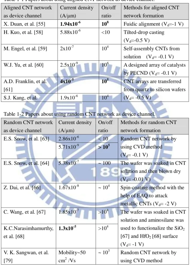
Table 1-1 Papers about using aligned CNT network as device channel……….11 Table 1-2 Papers about using random CNT network as device channel……….11
Chapter 3
Table 3-1 Summary of optimized CNT coating density for channel length ranging from 1.4 to 7 μm and channel width varying from 5 to 50 μm…………..43 Table 3-2 Summary of effects of CNT solution properties and device parameters on on-state current and on/off ratio……...……….…….43 Table 3-3 Comparison of simulation and experimental percolation threshold for
x
List of Figures
Chapter 1
Fig.1-1 (a) Scanning tunneling microscope (STM) image of a SWNT [4]. (b) Cross-section TEM images of MWNT with different sheets [2]………….12 Fig.1-2 Schematic description of the three types of SWNTs on the two-dimensional
graphene layer: zigzag, chiral, and armchair SWNTs [6]………...….13
Chapter 2
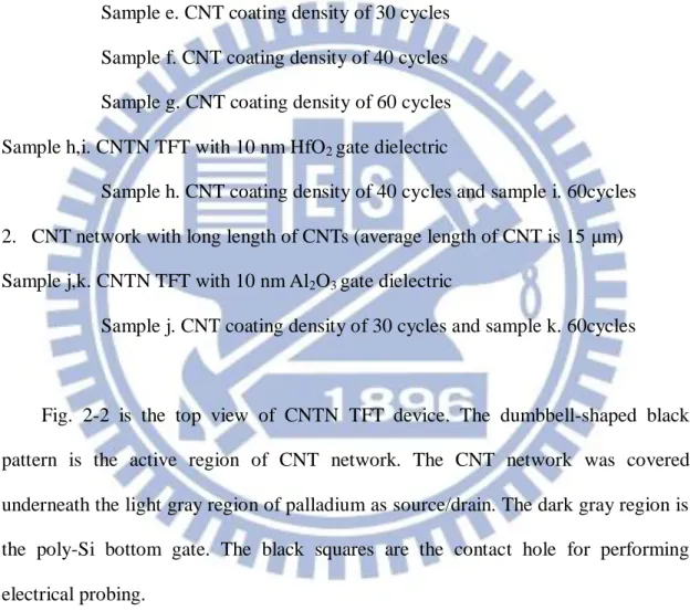
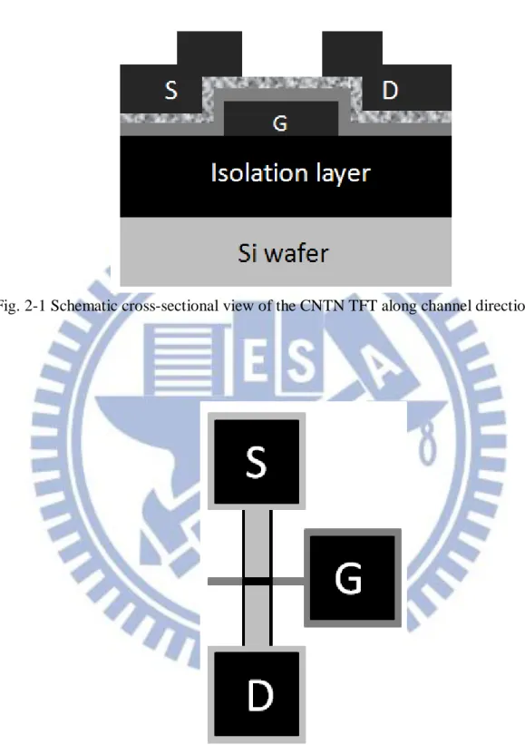
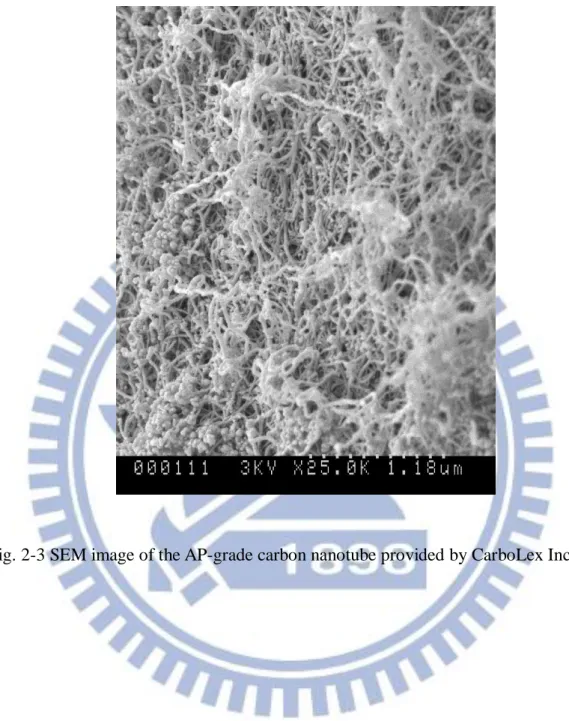
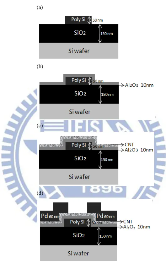
Fig. 2-1 Schematic cross-sectional view of the CNTN TFT along channel direction.21 Fig. 2-2 Schematic top-view of the CNTN TFT……….….21 Fig. 2-3 SEM image of the AP-grade carbon nanotube provided by CarboLex Inc ..22 Fig. 2-4 Process flows of the CNTN TFT. (a) SiO2 isolation layer and in-situ doped
poly Si gate definition (b) ALD Al2O3 gate dielectric layer and furnace
annealing for Al2O3 layer densification (c) bottom gate contact hole etching
and spin-coating CNT network (d) Pd source/drain formation by sputter deposition and lift-off method………..23 Fig. 2-5 SEM images of CNT coating 40 cycles on Al2O3 layer (a) 50k x
magnification (b) 80k x magnification……….24
Chapter 3
Fig. 3-1 SEM images of CNT networks with CNT coating density ranging from 20 to 60 cycles on Al2O3 film (a) 20 cycles (b) 30 cycles (c) 40 cycles (d) 60 cycles,
increasing CNT coating cycles results in the increase of CNT density…....44 Fig. 3-2 (a) SEM image of CNT network with CNT coating 60 cycles on HfO2 film.
xi
The poor wet ability of HfO2 film attributes low CNT network coverage.
(b)(c) SEM images of CNT network with 15-μm-long CNTs coating 30 cycles on Al2O3 film. It is noted that the CNT bundles are found. ((b) 6.5k x
and (c) 80k x magnification) (d) A large number of CNTs were coated on the substrate rather than the bottom gate due to geometrical rise………..……..45 Fig. 3-3 Transfer characteristics (Id vs. Vg) at Vd= -0.1V for devices with 10 nm Al2O3
gate dielectric layer (device dimension L= 0.4 μm and W= 50 μm) with CNT coating density varying from 20 to 60 cycles (a) CNT coating 20 cycles (b) CNT coating 30 cycles (c) CNT coating 40 cycles (d) CNT coating 60 cycles. All devices exhibit metallic behavior on this condition………46 Fig. 3-4 Transfer characteristics (Id vs. Vg) at Vd= -0.1V for devices with 10 nm Al2O3
gate dielectric layer (device dimension L= 1.4 μm and W= 50 μm) for CNT coating density varying from 20 to 60 cycles (a) CNT coating 20 cycles (b) CNT coating 30 cycles (c) CNT coating 40 cycles (d) CNT coating 60 cycles ………...47 Fig. 3-5 Transfer characteristics (Id vs. Vg) at Vd= -0.1V for devices with 10 nm Al2O3
gate dielectric layer (device dimension L= 4 μm and W= 50 μm) for CNT coating density varying from 30 to 60 cycles (a) CNT coating 30 cycles (b) CNT coating 40 cycles (c) CNT coating 60 cycles………48 Fig. 3-6 Transfer characteristics (Id vs. Vg) at Vd= -0.1V for devices with 10 nm Al2O3
gate dielectric layer (fixed channel width W= 50 μm) (a) L= 7 μm, CNT coating 40 cycles (b) L= 7 μm, CNT coating 60 cycles (c) L= 9 μm, CNT coating 60 cycles (d) L= 14 μm, CNT coating 60 cycles. All devices exhibit semiconducting behavior………....49 Fig. 3-7 On-state current vs. CNT coating density with various channel length L, fixed channel width W= 50 μm and Al2O3 gate dielectric thickness of 10 nm (a) L=
xii
0.4 μm (b) L= 1.4 μm (c) L= 4 μm (d) L= 7 μm. Increasing CNT coating density increases on-state current………..50 Fig. 3-8 On/off ratio vs. CNT coating density with various channel length L, fixed
channel width W= 50 μm and Al2O3 gate dielectric thickness of 10 nm (a) L=
0.4 μm (b) L= 1.4 μm (c) L= 4 μm (d) L= 7μm……….51 Fig. 3-9 On-state current against on/off ratio for various CNT coating density at varying channel lengths, fixed channel width W= 50 μm, and Al2O3 gate
dielectric layer of 10 nm (a) L= 1.4 μm (b) L= 4 μm (c) L= 7 μm. The blue line indicates On/off ratio = 100. Optimized CNT density are 20, 40, and 60 coating cycles for channel length L= 1.4, 4, and 7μm, respectively………..52 Fig. 3-10 CNT networks with CNT coating density of 30 cycles (a) on-state current vs.
channel length shows increasing channel length decreases on-state current nonlinearly. (b) on/off ratio vs. channel length shows increasing channel length improves on/off ratio. (c) on-state current vs. off-state current for various channel length (d) on-state current vs. on/off ratio for various channel length………..…53 Fig. 3-11 CNT networks with CNT coating density of 40 cycles (a) on-state current vs.
channel length (b) on/off ratio vs. channel length (c) on-state current vs. off-state current for various channel length (d) on-state current vs. on/off ratio for various channel length………..………..54 Fig. 3-12 CNT networks with CNT coating density of 60 cycles (a) on-state current vs.
channel length (b) on/off ratio vs. channel length (c) on-state current vs. off-state current for various channel length (d) on-state current vs. on/off ratio for various channel length.……….…..55 Fig. 3-13 Conducting percolation threshold (black line), metallic percolation threshold
xiii
0.4 to 14 μm. Devices exhibit metallic behavior when CNT density is above metallic percolation threshold. Besides, if devices exhibit semiconducting behavior, the yield is lower than 100%. There is a trade-off between 100% yield and metallic behavior………..………56 Fig. 3-14 CNT density and channel length dependence of on-state current and on/off
ratio are shown in 3D diagram. (a) on-state current- CNT density- channel length (b) on/off.………..…57 Fig. 3-15 Channel width dependence of on-state current and on/off ratio (device
dimension of fixed channel length L= 0.4 μm and width varying from W= 5 to 50 μm) (a) on-state current vs. CNT coating density (b) on/off ratio vs. CNT coating density. Decreasing channel width results in the decrease of on-state current and the improvement of on/off ratio……….…….58 Fig. 3-16 Channel width dependence of on-state current and on/off ratio (device
dimension of fixed channel length L= 1.4 μm and width varying from W= 5 to 50 μm) (a) on-state current vs. CNT coating density (b) on/off ratio vs. CNT coating density. It is noticed that increasing channel length would make on-state current decrease non-linearly due to nonuniform CNT network coverage. In addition, increasing channel length also improves on/off ratio significantly………..…59 Fig. 3-17 Channel width dependence of on-state current and on/off ratio (device
dimension of fixed channel length L= 4 μm and width varying from W= 5 to 50 μm) (a) on-state current vs. CNT coating density (b) on/off ratio vs. CNT coating density. The on/off ratio maintains a certain value which is not affected by channel width for devices with L= 4 μm………..60 Fig. 3-18 Channel width dependence of on-state current and on/off ratio (device
xiv
to 50 μm) (a) on-state current vs. CNT coating density (b) on/off ratio vs. CNT coating density. The on/off ratio is not affected by channel width for devices with L= 7 μm……….…..61 Fig. 3-19 On-state current plotted against on/off ratio for various CNT coating density at varying channel lengths and fixed channel width W= 20 μm, and 10 nm Al2O3 gate dielectric layer (a) L= 1.4 μm (b) L= 4 μm (c) L= 7 μm. The blue
line indicates On/off ratio = 100. Optimized CNT density are 30, 40, and 60 coating cycles for channel length L= 1.4, 4, and 7μm, respectively………..62 Fig. 3-20 On-state current plotted against on/off ratio for various CNT coating density at varying channel lengths and fixed channel width W= 5 μm, and 10 nm Al2O3 gate dielectric layer (a) L= 1.4 μm (b) L= 4 μm. Optimized CNT
density are 40 and 60 coating cycles for channel length L= 1.4 and 4μm, respectively………...63 Fig. 3-21 Gate dielectric thickness dependence on on-state current plotted against CNT coating density with various channel length L (a) L= 0.4 μm (b) L= 1.4 μm (c) L= 4 μm (d) L= 7 μm. Since device variation is larger than gate dielectric thickness change, decreasing gate dielectric thickness does not increase on-state current obviously………..64 Fig. 3-22 Gate dielectric thickness dependence on on/off ratio plotted against CNT coating density with various channel length L (a) L= 0.4 μm (b) L= 1.4 μm (c) L= 4 μm (d) L= 7 μm. Since device variation is larger than gate dielectric thickness change, decreasing gate dielectric thickness does not increase on/off ratio dramatically………65 Fig. 3-23 On-state current vs. on/off ratio for various CNT coating density at varying
channel lengths, fixed channel width W= 50 μm, and 5 nm Al2O3 gate
xv
indicates On/off ratio = 100. Optimized CNT density are 30, 40, and 60 coating cycles for channel length L= 1.4, 4, and 7μm, respectively…...….66 Fig. 3-24 Transfer characteristics (Id vs. Vg) at Vd= -0.1V for devices coated with
average CNT length of 15 μm. (a) CNT coating 30 cycles (b) CNT coating 60 cycles. Increasing CNT length results in the increase of on-state current significantly………..67 Fig. 3-25 Coating surface dependence (10-nm-thickness Al2O3 and HfO2) of on-state
current and on/off ratio (device dimension of L= 0.4 μm and W= 50 μm) (a) on-state current vs. CNT coating density (b) on/off ratio vs. CNT coating density. Poor wet ability of HfO2 film attributes low on-state current…...…68
Fig. 3-26 Coating surface dependence (10-nm-thickness Al2O3 and HfO2) of on-state
current and on/off ratio (device dimension of L= 1.4 μm and W= 50 μm) (a) on-state current vs. CNT coating density (b) on/off ratio vs. CNT coating density. Devices with HfO2 film improves on/off ratio with channel length L=
1.4 μm……….……69 Fig. 3-27 Percolation threshold for devices with fixed W= 50 μm and channel length varying from L= 1.4, 4, to 7 μm, respectively. (a) percolation threshold is 125 (CNTs) /70 μm2 = 1.79 CNTs/μm2 for L= 1.4 μm (b) 550 (CNTs)/ 200 μm2
= 2.75 CNTs/μm2 for L= 4 μm (c) 1050 (CNTs)/ 350 μm2 = 3 CNTs /μm2 for L= 7 μm………..………...70 Fig. 3-28 Mobility was plotted against channel length for devices with channel width
W= 50 μm and Al2O3 film of 10 nm for CNT coating density ranging from
20 to 60 cycles (a) CNT coating 20 cycles (b) CNT coating 30 cycles (c) CNT coating 40 cycles (d) CNT coating 60 cycles. Increasing channel length decreases mobility………...71 Fig. 3-29 Mobility was plotted against channel length for devices with channel width
xvi
W= 50 μm and Al2O3 film of 5 nm for CNT coating density ranging from 20
to 60 cycles (a) CNT coating 20 cycles (b) CNT coating 30 cycles (c) CNT coating 40 cycles (d) CNT coating 60 cycles. Increasing channel length decreases mobility.………...72 Fig. 3-30 Mobility was plotted against channel length for devices with channel width
W= 50 μm and HfO2 film of 10 nm for CNT coating density ranging from 40
to 60 cycles (a) CNT coating 40 cycles (b) CNT coating 60 cycles………..73 Fig. 3-31 Transfer characteristics (Id vs. Vg) before and after applying adapted
electrical breakdown method (device dimension of channel length L= 0.4 and 1.4 μm, fixed channel width W= 50 μm, and Al2O3 film of 5 nm) (a) L=
0.4 μm (b) L= 1.4 μm. By performing electrical breakdown method, on/off ratio improves 2 orders of magnitude……….……….74 Fig. 3-32 Transfer characteristics (Id vs. Vg) before and after applying adapted
electrical breakdown method (device dimension of channel length L= 0.4 and 1.4 μm, fixed channel width W= 50 μm, and Al2O3 film of 10 nm) (a)
L= 0.4 μm (b) L= 1.4 μm. On/off ratio improves more than 2 orders of magnitude with the increase of gate dielectric thickness……….75
1
Chapter 1
Introduction
1-1 Fundamental Properties and Fabrication of Carbon
Nanotubes
In 1985, R. Smalley, H. Kroto, and R. Curl found C60 molecule formed by
performing laser irradiation to vaporize graphite [1]. This carbonaceous product has a truncated icosahedrons structure, which is commonly considered as the football called buckyball. This C60 molecule has a stable structure which all sites are satisfied with
one double bond and two single bonds. The discovery of C60 caught researcher’s eyes
and made significant study of carbonaceous product.
In 1991, S. Iijima, a researcher of NEC corporation, first found multi-walled nanotubes (MWNTs) in fullerene synthesis [2]. MWNTs have hollow cylinder structure consisting of multiple concentric shells of graphite. Soon after the discovery of MWNTs, in 1993, Iijima discovered single-walled nanotubes (SWNTs) grown by using transition metals as catalysts [3].
Carbon nanotubes (CNTs) are hollow cylinder structures with diameter verying from 1 to several nm and length up to tens of μm. We can imagine that CNTs are made by wrapping graphene sheets to tube structures. There are two types of CNTs including single-walled nanotubes (SWNTs) and multi-walled nanotubes (MWNTs) shown in Fig. 1-1 [2,4]. The diameter of a SWNT is usually 1-2 nm whereas the diameter of a MWNT is ranging from 1 nm to hundreds of nm depending on the number of graphite shells with the spacing of 0.34 nm between each interlayer [5]. The characteristics of MWNTs are hard to analyze due to the complex interaction of
2
multiple shells. In addition, CNT bundles could be formed owing to van der Waals force between successive graphene layers.
The diameter and the way graphite layer wrapped of SWNT are defined uniquely by the chiral vector c= na1+ ma2, which denoted as (n,m) indices on
two-dimensional graphene layer, where a1 and a2 are lattice vectors and (n,m) are
integers shown in Fig. 1-2 [6-7]. SWNTs exhibit metallic or semiconducting behavior which are affected by (n,m) indices. There are three types of SWNTs including zigzag, chiral and armchair SWNTs. Zigzag (n,0) SWNTs which the index of m= 0 could exhibit metallic behavior as n/3 is an integer, otherwise zigzag SWNTs exhibit semiconducting behavior. Chiral (n,m) SWNTs also can have metallic or semiconducting behavior, when (2n+m)/3 is an integer, SWNTs exhibit metallic behavior and in other cases of (n,m) semiconducting SWNTs exist. Armchair (n,n) SWNTs which the index of m= n only exhibit metallic behavior. The calculation results derived from electronic band structure also confirmed that about l/3 SWNTs are metallic and 2/3 SWNTs are semiconducting [8-9]. The diameter of SWNTs is defined as d =|c|
π = a π n1
2+ n
1n2+ n22, where a= 0.246 nm, which is the unit vector of graphene lattice [8]. In addition, the band gap is inversely linear proportion to the diameter of SWNTs [4,10].
CNTs could be synthesized by various methods such as arc discharge [11], laser ablation [12-13], and chemical vapor deposition (CVD) [14-16].
The arc discharge method was performed to form the fullerenes in the beginning and is a simple way to produce CNTs. The reaction chamber is filled with inert gas at low pressure. The high temperature discharge occurs between two carbon electrodes by applying high potential difference. The discharge would vaporize and consume the positive carbon electrode. On the other hand, the carbonaceous products containing
3
CNTs are produced in the negative electrode. The product formed in this method is a complex mixture containing both SWNTs and MWNTs with some defects and catalysts. Thus, the purification is needed. The yield is low and depends on the gas pressure in the reaction chamber and the temperature of discharge.
The laser ablation method is conducted by using a laser pulse to vaporize the target which is a mixture of graphite and metal catalyst particles such as cobalt or nickel in the chamber filled with inert gas. As the carbonaceous vaporization condenses, SWNTs are formed on the cool surface. This method is with high yield of 70% and synthesizes SWNTs with controllable diameter and better quality. The diameter of SWNTs could be defined by tuning the growth temperature and catalyst composition. However, it is much expensive than arc discharge and CVD method.
The principle of chemical vapor deposition (CVD) method is that by feeding process gas such as hydrogen and carbonaceous gas such as methane or ethylene into reaction chamber, CNTs would grow at the location of metal catalysts on the substrate at high temperature. The diameter of CNTs depends on the size of metal catalysts [17]. In addition, the alignment of CNTs can be realized by applying electric field on silicon substrate with patterned metal catalysts [18] or on single crystal quartz substrate [19]. The CVD method is suitable for large scale production for commercial industry to decrease the cost of SWNT production.
1-2. Potential Applications of CNTs
CNTs have various potential properties such as one-dimensional transport , extraordinary electrical, thermal, mechanical, optical, and chemical property, which are attractive and studied in many applications including TFTs [20-21], diodes [21], logic circuits [22], optical modulators [23], strain-sensing devices [24], chemical
4 [25-26] and biological [27-28] sensors.
The metallic CNTs could carry electric current density of 4 × 10⁹ A/cm2, which is 1000 times larger than copper [29]. CNTs exhibit high thermal conductivity of 3500 Wm-1K-1 along the tube direction, comparing to thermal conductivity of copper of 385 Wm-1K-1[30-31]. In addition, it is also an insulator with thermal conductivity of 1.52 Wm-1K-1 across the tube direction. CNTs have tensile strength of 63 GPa and are remarkably flexible with high elastic modulus due to formation of sp2 bond [32-33].
1-3. Electrical Characteristics of CNTFET with Single SWNT
In 1998, the first carbon nanotube field-effect transistor (CNTFET) consisting of one semiconducting SWNT as channel connected to metal S/D was fabricated [34-35]. The fabrication of this single molecule device realizes the potential for next generation of molecular electronics. Nowadays, CNTFETs exhibit high mobility of 100000 cm2/Vs [36], current carrying capacity > 109 A/cm2 [37], on/off ratio > 106 [38], and subthreshold swing < 80 mV/decade [39].In an ambient environment, the semiconducting CNTs usually exhibit p-type behavior [37] since the adsorbed oxygen on CNT surface results in the modification of the Schottky barriers between metal contacts and CNT [40]. The location of Fermi level pinning is close to the valence band. Studies also showed that the conversion from p-type to n-type CNTTFT could be done by doping CNTs with alkali metals [41-42] or polyethylene (PEI) [21,43] to change barrier thickness and shift the threshold voltage, or anneal CNTTFTs [40] to remove adsorbed oxygen. It is noticed that oxygen modifies the barrier at contact rather than dopes the bulk of tube. The oxygen would oxidize the metal contact and then changes the charge transfer from metals. In addition, by lining up the valence or conduction band of CNTs to Fermi
5
level of metal contact, for instance, palladium (Pd) for p-type and scandium (Sc) for n-type CNTTFT were demonstrated [37,44].
The electrical characteristics of CNTTFT would be affected by various factors such as chirality and diameter of CNTs [45], types of metal contacts [46], environmental conditions. The band gap of CNT is inversely proportion to the diameter of CNTs and different chirality of CNTs contributes to metallic or semiconducting behavior. Choosing proper metals which have strong interaction with carbon results in good contact between S/D and CNTs. CNTTFTs are also sensitive to environmental conditions such as gas type, vapor, and vacuity. Charge transfer occurs from adsorbed gas molecules to CNTs [47-49] and water vapors contribute the hysteresis of CNTTFT due to charge trapping by water molecules around the CNTs [50-52]. In addition, the irradiation of electrical beam would damage CNT structure and decrease the conductivity of CNTs [53-54]. Although CNTTFTs with individual SWNT exhibit superior performance, the large variation of electrical characteristics between each device hurdles the development of CNTTFTs which are not suitable for large scale production.
1-4. Percolating CNT network TFT
In order to minimize the variation between each SWNT, TFTs based on SWNT networks consisting of large number of SWNTs rather than individual SWNT are fabricated to average individual SWNT deviation by SWNT networks. In 2003, Duan et al. proposed TFTs fabricated with aligned CNTs as channel by using flow-directed alignment method [55]. This work offered a new direction for high performance TFTs. Since then, many studies of CNT network TFT are published.
6
orient. Y. Huang showed that parallel CNT array could be formed by using fluidic alignment and flow direction control with surface-patterning of PDMS mold [56]. CNT orientation also could be controlled by the direction of gas flow with a tilt angle [57-58]. M. Engel used evaporation self-assembly method to orient CNT arrays [59]. The CNT array also could be fabricated on a designed array of catalysts by using PECVD [60]. A.D. Franklin proposed aligned CNT array FETs with current density > 40 uA/μm at on/off ratio >105 [61], however, the CNT array needed to transfer from quartz to silicon wafers. This CNT transfer process preserved CNT density and alignment by using thermal release adhesive tape, but the process was complex and unsuitable for large scale manufacture [62]. The drawback of aligned CNT network is that the assembling process is complex and lack of precise control of CNT alignment. Although CNT arrays would align along specific direction, intersections between CNTs still exist. Papers listed above about aligned CNT network as device channel are shown in Table 1-1.
Due to the simplicity for the formation of CNT network, random CNT network TFTs which CNTs orient with no preferential directions are suitable for large scale fabrication. A large number of CNTs average deviation of individual CNT. E.S. Snow reported a random SWNT networks TFTs with field-effect mobility of 10 cm2/Vs at on/off ratio > 105 for low CNT density and field-effect mobility > 100 cm2/Vs at on/off ratio < 10for high CNT density [63-64]. CNT powder dissolved in SDS [65] or EAQ/DMF [66] solution with gradient ultracentrifugation were used to separate CNT bundles and improved the uniformity of CNT networks formed by spin-coating method. In addition, aminosilane such as aminopropyltriethoxy silane (APTES) was used to functionalize the SiO2 [67] and HfOx [68] surface to achieve high density and uniform CNT network due to its well-known affinity to the CNTs.
7
method. However, about 1/3 metallic and 2/3 semiconducting CNTs both exist in network. Once metallic CNT conducting paths bridge channel, the on/off ratio would significantly degrades. Recently some works studied percolation theory [69-71] which was studied in the formation of CNT conducting paths in the network. J. N. Coleman reported an organic composite consisted of mixture of organic polymer and CNTs [72]. The CNT concentration increased with the significant increase of conductivity of organic composite which was in agreement of percolating behavior. L. Hu studied the sheet conductance and transparency of CNT network as a function of CNT density [73]. When the CNT density is above the percolation threshold, conductivity of CNT network increases obviously. This means the CNT conducting paths are formed. On the other hand, the percolation theory is not suitable for study of optical transparency of CNT network since transparency is determined by CNT excitation rather than CNT conductance. H. E. Unalan found that device performance of CNT TFT is limited by metallic CNTs as percolation density of metallic CNTs is much below percolation threshold of conducting paths [74]. S. Kumar studied a computational model containing ballistic and diffusive transport limit to analysis the conductance of CNT network [75]. A. Behnam performed Monte Carlo simulations to study the geometry-dependant resistivity of CNT films and found that the lowest resistivity occured in the partially aligned CNTs rather than perfectly aligned CNTs [76]. J. Hicks reported the CNT length distribution dependent on the resistivity for junction-resistance-dominant and intrinsic-resistance-dominant CNT networks, respectively [77]. S. Seppälä computed percolating network of CNT bundles due to van der Waals interaction for varying bundle length and bundle density. This work discovered semiconducting CNT bundle paths were more frequently formed for low density comparing with ordinary SWNT networks [78]. V. K. Sangwan performed experiments and simulations to determine that the percolating CNTTFT with mobility
8
of 5~50 cm2/Vs at on/off ratio > 103 at L > 70 μm and W= 50 μm for CNT density of 0.54~0.81 CNTs/μm2 [79]. Table 1-2 shows papers discussing random CNT networks as device channel.
1-5. Motivation
Recently, most percolation issues were emphasized on the conductance of CNT network rather than device performance of CNT network TFTs. Although some studies showed experimental electrical characteristics of devices fabricated with CNT percolating networks, a few works focused on the analytical study of properties of CNT networks TFT. This thesis systematically studied the effects of CNT property and device geometry on device performance based on CNT networks for both experiments and simulations. By studying the percolating CNT network with proper fabrication condition and device structure, the suitable device design and control could be obtained.
This thesis studies the carbon nanotube network thin film transistor (CNTN TFT) structure consisting of an extra poly-Si gate as local bottom gate instead of using heavily-doped Si substrate as a back gate. The merit of back gate structure is easy to fabricate. However, the back gate structure would not control each device on whole wafer respectively at single operation. Besides, devices with back gate structure need thicker gate dielectric layer to prevent gate leakage since that source/drain is totally overlapped by back gate. But increasing gate dielectric thickness would degrade the gate-to-channel control ability.
To improve the drawback of back gate structure, some papers proposed the idea of top-gated CNT TFT [39]. Though top gate structure would control each device respectively, the surface coverage of top gate dielectric layer and gate leakage are
9
severe issues. First, the gate dielectric would not be formed by thermal oxide since the CNT network which belongs to back-end process is formed prior to gate dielectric. Other methods to form gate dielectric layer would be sputter, plasma enhanced chemical vapor deposition (PECVD), E-gun evaporation, atomic layer deposition (ALD), and so on. But note that for some process such as PECVD would strongly damage CNTs by plasma bombardment. G. Zhang presented a plasma hydrocarbonation reaction to selectively etch metallic CNTs and remain semiconducting CNTs [80]. The key process to selective etch metallic CNTs was to use methane plasma instead of hydrogen plasma due to its moderate reactivity.
Recently ALD is a popular process to form the gate dielectric to cover on CNT network. However, ALD process is still difficult to grow high quality of thin film on CNT network since the chemical inert exterior surface of CNTs would retard the precursor to absorb on. Therefore, to form perfect ALD gate dielectric layer on CNT network needs another CNT functionalization to improve the surface coverage of top gate dielectric layer and prevent gate leakage. B Damon made NO2 functional group
attach to nanotube surface to improve the ALD Al2O3 layer uniformity due to the
reactivity of precursors enhencement [81-82].
The second issue of top gate structure is gate leakage. In order to avoid damaging CNTs, the source/drain fabrication also needs to prevent CNTs exposing in the plasma atmosphere. Therefore, the metal source/drain definition process is performed by lift-off method rather than metal dry etching. The disadvantage of lift-off method is the sharp edge of source/drain affects the conformal ALD gate dielectric and makes gate dielectric locally thinner near sharp edge of source/drain. This locally sharp region further enhances the electric field and then increases the probability of gate leakage.
10
horizontal furnace of front-end process is studied. Bottom gate structure would eliminate the gate dielectric coverage issue since the gate dielectric formation is prior to CNT network fabrication. There is no need to employ other functionalization to CNTs. The reduction of overlap between bottom gate and source/drain could decrease the parasitic capacitance and scale the gate dielectric thickness to operate device at low operation voltage. Besides, devices with bottom gate structure would control single device at single operation.
1-6. Thesis Organization
The first chapter is the introduction including fundamental properties of CNTs, the CNT fabrication methods, and various applications using CNTs. Then, the review of individual CNT TFT and percolating random CNT network TFT are discussed. The second chapter shows the device structure of CNTN TFT, experimental settings and process flow.
Experiment results are discussed in the third chapter. Firstly, the CNT network distribution and various CNT densities corresponding to spin-coating cycles were determined by scanning electron microscopy (SEM) images. Electrical characteristics such as on-state current, on/off ratio, and field-effect mobility were conducted to study the following effects of CNT density and length, channel length and width dependence, gate dielectric thickness, and coating surface consisted of Al2O3 and
HfO2 on the device performance. The Monte Carlo simulation of percolating CNT
network was also performed to determine percolation threshold with varying CNT density and device channel length. Finally, the adapted electrical breakdown is introduced to improve on/off ratio. The last chapter is the summary and future works of this thesis.
11
Table 1-1 Papers about using aligned CNT network as device channel. Aligned CNT network as device channel Current density (A/μm) On/off ratio
Methods for aligned CNT network formation
X. Duan, et al. [55] 1.94x10⁻⁶ 108 Fuidic alignment (Vd=-1 V)
H. Kuo, et al. [58] 5.88x10⁻⁶ <10 Tilted-drop casting (Vd=-0.5 V)
M. Engel, et al. [59] 2x10⁻⁷ 104 Self-assembly CNTs from solution (Vd= -0.1 V)
W.J. Yu, et al. [60] 2.5x10⁻⁹ 106 A designed array of catalysts by PECND (Vd= -0.1 V)
A.D. Franklin, et al. [61]
4x10⁻⁵ 105 CNT arrays are transferred from quartz to silicon wafers (Vd= -0.5 V)
S.J. Kang, et al. 1.9x10⁻⁶ 104
Table 1-2 Papers about using random CNT network as device channel. Random CNT network as device channel Current density (A/μm) On/off ratio
Methods for random CNT network formation E.S. Snow, et al. [63] 2.86x10⁻⁶ < 10 Random CNT network by
using CVD method (Vd= -0.1 V)
5.71x10⁻⁹ > 105
E.S. Snow, et al. [64] 5.38x10⁻⁷ ~ 100 The wafer was soaked in CNT solution and then blown dry (Vd= -0.01 V)
Z. Dai, et al. [66] 1.67x10⁻⁸ ~ 104 Spin-coating method with the help of EAQ to attack
metallic CNTs (Vd= -2 V)
C. Wang, et al. [67] 1.85x10⁻⁷ >104 The wafer was soaked in CNT solution and aminosilane was used to functionalize the SiO2
[67] and HfO2 [68] surface
(Vd= -1 V) K.C.Narasimhamurthy, et al. [68] 1.3x10⁻⁵ >104 V. K. Sangwan, et al. [79] Mobility~50 cm2 /Vs ~ 103 Random CNT network by using CVD method
12 (a)
(b)
Fig. 1-1 (a) Scanning tunneling microscope (STM) image of a SWNT [4]. (b) Cross-section TEM images of MWNT with different sheets [2].
13
Fig. 1-2 Schematic description of the three types of SWNTs on the two-dimensional graphene layer: zigzag, chiral, and armchair SWNTs [6].
14
Chapter 2
Experimental Settings and Device Fabrication
2-1 Device Structure of CNTN TFT
Fig. 2-1 shows the CNTN network with bottom gate structure. First, a SiO2
isolation layer was formed. Then, the in-situ doped N+ poly-Si bottom gate was defined and a 900 °C, 20 seconds RTA was performed to activate dopant of poly-Si. Atomic layer deposition (ALD) was performed to deposit Al2O3 and HfO2 layer as
gate dielectric respectively and then a 700°C, 30 minutes N2 annealing was performed
for Al2O3 layer densification. After the contact hole etching by dipping wafers in BOE
solution, CNT network was formed by spin-coating method and defined by O2 plasma.
The CNT powder was dissolved in dimethylformamide (DMF) solution with 24-hours-socication for preparation. Finally, the palladium (Pd) source/drain was formed by lift-off process. Palladium had good interaction with CNTs and due to its high work function, the ohmic contact was formed between palladium and CNTs to reduce the barrier of hole transport [105]. Source/drain deposition after CNT network formation would reduce the gate leakage due to locally sharp edge of source/drain caused by metal source/drain lift-off method. The details of process flow would be described in section 2-4.
2-2 Experimental Settings
This thesis studies CNTN TFT with bottom gate structure. Devices are listed as following for electrical characterization:
15
Sample a-d. CNTN TFT with 10 nm Al2O3 gate dielectric
Sample a. CNT coating density of 20 cycles Sample b. CNT coating density of 30 cycles Sample c. CNT coating density of 40 cycles Sample d. CNT coating density of 60 cycles Sample e-g. CNTN TFT with 5 nm Al2O3 gate dielectric
Sample e. CNT coating density of 30 cycles Sample f. CNT coating density of 40 cycles Sample g. CNT coating density of 60 cycles Sample h,i. CNTN TFT with 10 nm HfO2 gate dielectric
Sample h. CNT coating density of 40 cycles and sample i. 60cycles 2. CNT network with long length of CNTs (average length of CNT is 15 μm) Sample j,k. CNTN TFT with 10 nm Al2O3 gate dielectric
Sample j. CNT coating density of 30 cycles and sample k. 60cycles
Fig. 2-2 is the top view of CNTN TFT device. The dumbbell-shaped black pattern is the active region of CNT network. The CNT network was covered underneath the light gray region of palladium as source/drain. The dark gray region is the poly-Si bottom gate. The black squares are the contact hole for performing electrical probing.
In this thesis, there are 8 sizes of channel length for mask layout: ranging from 0.4, 1.4, 4, 7, 9, 14, 29 to 49 μm. The channel widths of 5 μm, 20 μm, 50 μm are defined. For channel length of 0.4 μm and 1.4 μm, the source/drain to gate overlap is 0.3 μm. For other dimensions of channel length, the source/drain to gate overlap is 0.5 μm. Therefore, the gate lengths of devices are 1, 2, 5, 8, 10, 15, 30 and 50 μm respectively.
16
2-3 Carbon Nanotube Solution Makeup
The AP-Grade carbon nanotube powder was commercially obtained from CarboLex Inc. The carbon nanotbes were made by arc discharge method which produced both single and multi-walled nanotubes (MWNT). Since the AP-Grade carbon nanotube powder was not performed by any chemical treatment, the quality of CNTs is high and the purity of CNTs is between 50 to 70 vol%. The residual catalyst impurities are nickel (Ni) and yttrium (Y). There are 66.7% semiconducting SWNT and 33.3% metallic SWNT with diameter 1.4 nm and length about 1.4 μm. The diameter of CNT bundle is 20 nm. Fig. 2-3 shows the SEM image of AP-grade carbon nanotube provided by CarboLex Inc.
The carbon nanotube powder of 1 mg was dissolved in 40 ml dimethylformamide (DMF) solution which is very effective on separating and suspending CNTs. Note that if the concentration of CNT powder > 0.025 mg/ml, the concentration of CNT solution would exceed the saturation concentration and then deposit CNT residues. These residues of CNT bundles would make the CNT network non-uniform after employing spin-coating and then affect device electrical characterization. After dissolving the CNT powder in DMF solution, a 24-hours of sonication was performed to separate the tangled CNT bundles. The duration of sonication would not be longer than 24 hours to avoid the length reduction of CNT and the CNT quality degradation.
2-4 Process Flow
The details of process are showed in Fig. 2.4: 1. Laser marking of 6-inch Si wafer
17
Corp. Then laser marker NEC SL473D2 was used to mark the wafers for label. To remove the particles produced by laser marking, an standard clean 1 (SC-1) which is the cleaning process of soaking wafers into solution containing NH4OH : H2O2 : H2O
= 1 : 4 : 20 for 600 seconds at 75 °C was performed after laser marking. 2. Pre-furnace standard (STD) clean and wet oxide 150nm
Before the wet oxidation, the wafers were performed the STD clean. The STD clean contains SC-1 and SC-2. The DI water rinse was performed before and after each clean. SC-2 is the cleaning process of soaking wafers into solution containing HCl : H2O2 : H2O = 1 : 1 : 6 for 600 seconds at 75 °C. After the STD
clean, the wet oxidation of 150 nm SiO2 isolation layer was grown at 980 °C by
horizontal furnace.
3. Pre-furnace STD clean and in-situ doped N+ poly Si 50 nm
If this deposition process was subsequent to previous process, the STD clean could be skipped. Otherwise, after the pre-furnace STD clean, in-situ doped N+ poly Si layer of 50-nm-thickness was formed by vertical furnace and used for bottom gate. 4. RTA process for dopant activation of in-situ doped N+ poly Si bottom gate
After in-situ doped N+ poly Si formation, the HEATPAULSE AG-610i system was used for 900 °C rapid thermal annealing (RTA) process for 20 seconds. The RTA process was performed to activate PH3 dopant of in-situ doped N+ poly Si layer and
made the grain size grow to reduce the gate resistance. 5. Bottom gate patterning
The lithography process was performed by TEL CLEAN TRACK MK-8 for photo resist (PR) coating and development. The Canon FPA-3000i5+ Stepper was used for exposure. After the lithography process, the 50 nm poly-Si bottom gate was patterned by TCP 9400SE poly etcher. The Mattson AspenII Asher was used to remove the PR residue by O2 plasma when patterning process was completed.
18
6. RCA clean and ALD 10 nm Al2O3 and HfO2 gate dielectric layer respectively
Before gate dielectric layer was formed, the RCA clean was performed to remove contaminants and native oxide from wafer surface. Cambridge NanoTech Fiji-202 DC system was used to atomic layer deposition (ALD) process. There were two split conditions for gate dielectric layer: one was Al2O3 and another was HfO2 layer.
Trimethylaluminium (TMA) and H2O were the ALD precursors for Al2O3 layer.
Tetrakis(ethylmethylamino)hafnium (TEMAH) and H2O were precursors for HfO2
layer. Then each wafer put in a 8-inch chuck at 250 °C. The deposition cycle was composed of one H2O pulse and one TMA/TEMAH precursor pulse. The
10-seconds-wait and pumping were performed after each pulse to remove reaction byproducts and residual precursors. The ALD deposition rate were 0.99 Å per cycle for Al2O3 layer and 0.85 Å per cycle for HfO2 layer respectively.
7. Horizontal furnace annealing for ALD Al2O3 layer
After ALD Al2O3 deposition, a 30 minutes, 700 °C, N2 annealing was performed
to densify Al2O3 layer and decrease the gate leakage by horizontal furnace. The HfO2
layer was not performed annealing process since high-temperature-annealing might cause HfO2 agglomeration to increase gate leakage.
8. Bottom gate contact hole etching
After the I-line lithography process, the wafers were soaking in buffered oxide etchant (BOE) solution containing NH4F : Hf = 6 : 1 for 10 seconds to etch the 10 nm
Al2O3 layer. Then wafers were sonicated in acetone for 5 minutes to remove the
residual photo resists.
9. CNT network formation by spin-coating method
The details of CNT solution preparation is described in section 2-3. The 1 mg CNT powder was dissolved in 40 ml DMF solution with 24-hours-socication. Then, using a burette to drop about 0.1 ml CNT solution and a 2-step spin-coating was
19
performed by Synrex 1-PM101D-R790 photo resist spinner. The first step was with rotation speed of 500 rpm for 10 seconds to make CNT solution spread on the wafer uniformly. The second step was with 2500 rpm rotation speed for 20 seconds to remove residual solution on the wafer. After the spin-coating, wafers were baked on the hot-plate for 120°C, 180 seconds to evaporate DMF residues which would affect device electrical characteristics.
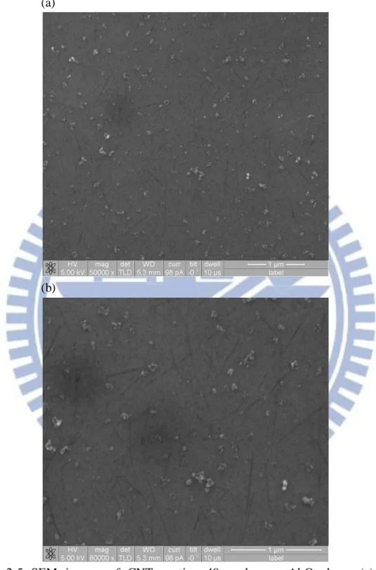
The high rotation speed of second step would affect the number of CNTs on the device channel. The higher the rotation speed was, the less the number of CNTs were on the channel. Fig. 2-5 shows the SEM image of CNT coating 40 cycles on Al2O3
film. The CNT network was spread on the wafer without any aggregation. From the SEM image we can derive the coverage rate of CNT network is about 1% since the coverage area of single CNT is equal to 1.4 nm CNT diameter times CNT length. Fig. 2-5 also shows that the CNT length is ranged from 0.3 μm to 1.4 μm due to some broken CNTs caused by sonication.
10. CNT stripe definition by O2 plasma
The lithography process of CNT network was performed by I-line lithography system. The Anelva ILD-4100 Metal etcher was used to define the CNT stripes by O2
plasma. The photoresists were covered on the device active region and then the O2
plasma was used to remove CNTs which were not protected by photoresists. The CNT network patterned to CNT stripes would further define the channel region precisely. After the patterning process, the wafers were sonicated in acetone for 2 minutes to remove the residual photo resist.
11. 60 nm Pd source/drain patterning by sputter deposition and lift-off method After the lithography process using I-line lithography system, the 60 nm
palladium (Pd) source/drain were deposited by Ion Tech Microvac 450CB sputter system. The DC sputter process under Ar gas of 24.4 sccm was performed with
20
pressure 7.6 mbar. The deposition rate is 0.78 nm per minute with DC power of 17 W. The residual photo-resist and metal were sonicated in acetone for 10 seconds by lifted-off method. Then the whole process was finished.
21
Fig. 2-1 Schematic cross-sectional view of the CNTN TFT along channel direction.
22
23 (a)
(b)
(c)
(d)
Fig. 2-4 Process flows of the CNTN TFT. (a) SiO2 isolation layer and in-situ doped
poly Si gate definition (b) ALD Al2O3 gate dielectric layer and furnace annealing for
Al2O3 layer densification (c) Bottom gate contact hole etching and spin-coating CNT
24 (a)
(b)
Fig. 2-5 SEM images of CNT coating 40 cycles on Al2O3 layer (a) 50k x
25
Chapter 3
Results and Discussion
3-1 Scanning Electron Microscopy (SEM) Analysis of CNT
Networks
FEI Nova 200 Dual beam (focused ion beam and electron beam) System (FIB/SEM) was performed to observe the dispersion and coating density of CNT networks. The accelerate voltage is 5 kV. The dual beam FIB/SEM system is with high solution since pure metal would occur field emission in high electric field to enhance resolution limit.
The SEM images were used to analyze the effect of CNT coating density, average CNT length and coating surface types on CNT network coverage. In addition, the number of CNTs on device channel was also shown in SEM images.
Fig. 3-1a to 3-1d show the CNT networks on the active channel region with Al2O3 surface for 1-μm-long CNT coating density ranging from 20 to 60 cycles. The
CNTs were dispersed without aggregation on Al2O3 film. By approximately counting
the number of CNTs in the 3.2 μm × 2.5 μm channel area in Fig. 3-1a to 3-1c, the CNT density were 2.13, 3.75, and 6.5 CNTs/μm2, respectively. Note that lighter CNTs (white CNTs) occur in the dense network for CNT coating density of 60 cycles in Fig 3-1d rather than dark CNTs shown in Fig 3-1a to 3-1c. For SEM analysis, the lighter images exhibit the higher conductivity. This suggests that increasing CNT density increases the electrical conduction in the CNT network.
For the SEM images of Fig. 3-1a to 3-1d, increasing CNT coating cycle would increase the number of CNTs and CNT conducting paths in the channel. In addition,
26
the catalyst particles and carbon residues increase with the increase of CNT coating density.
Besides the CNT density, the coating surface property is also a crucial factor to affect the CNT network dispersion. For the same concentration of CNT solution and spin condition, the CNT density is much lower on the HfO2 surface (~ 0.63 CNT/μm2)
shown in Fig. 3-2a. The sparse network is due to the poor wet ability of HfO2 film
which also affects the electrical characterization discussed in section 3-3.
In Fig 3-2b and 3-2c, the long CNT networks with average CNT length of 15 μm were formed instead of short CNTs of 1 μm shown in Fig 3-1. The CNT conducting paths were formed up to tens of μm. Thus, the lower CNT coating density of 30 cycles was able to bridge source and drain in channel length L= 50 μm. However, the bundled CNTs rather than single CNTs occurred in Fig. 3-2(c) to affect the device electrical properties for long length CNTs.
Fig. 3-2d shows that there were a large number of CNTs on the substrate rather than on the bottom gate since the height of 50 nm between bottom gate and substrate would hinder CNTs on the channel during spin-coating method. The geometrical rise of bottom gate would decrease the CNT network density in the channel region and cause non-uniform CNT dispersion for devices with channel length L > 4 μm.
3-2 Effects of CNT Properties and Device Parameters - Al
2O
3Gate Dielectric
The electrical characterization of CNTN TFTs was conducted in ambient condition using the probe station of Cascade Microtech Inc and Agilent 4156C semiconductor parameter analyzer. Device characteristics were measured and used to analyze device on-state current, off-state current, on/off ratio and effective field-effect
27 mobility in linear region.
This thesis studies the following effects on CNTN TFT device performance: 1. CNT density
2. Channel length dependence ranging from 0.4 to 14 μm 3. Channel width dependence ranging from 5 to 50 μm 4. Gate dielectric thickness
5. CNT length
6. Coating surface types including Al2O3 and HfO2 gate dielectric layer
We measured 12 devices with same device dimension for each factor mentioned above to average the individual deviation of CNTN TFTs and then the statistical diagrams were performed to analyze each effect which affects device performance.
The gate voltage (Vg) swept from -4 V to 4 V for devices with 10 nm Al2O3 layer
to obtain the Id-Vg transfer characteristics at Vd= -0.1 V since the CNTN TFTs
proposed in this thesis exhibit p-type behavior.
Fig. 3-3 to 3-6 show the Id-Vg characteristics of CNTN TFTs with various channel length L= 0.4 – 14 μm and fixed channel width W= 50 μm for CNT coating density varying from 20 to 60 cycles. The CNT density increases by increasing the number of spin-coating cycles of CNT solution.
The transfer characteristics are divided roughly into two cases, one extreme case is shown in Fig 3.3 with high on-state current of 10-5 A and low on/off ratio < 10, and another extreme case shown in Fig 3.6 with low on-state current of 10-8 A and high on/off ratio > 103. In between these two extreme cases, other transfer characteristics shown in Fig. 3-4 and 3-5 depend on the interaction between CNT coating density and channel length. CNTN TFTs with the same CNT coating density and device dimension could exhibit either metallic or semiconducting behavior since CNT conducting paths in channel were mixed with both metallic and semiconducting CNTs.
28
Once the conducting path contains one semiconducting CNT at least, the conducting path exhibits the semiconducting behavior with high on/off ratio.
3-2.1 Effect of CNT Density
In order to further analyze the effect of CNT density on on-state current and on/off ratio, the transfer characteristics measured in Fig. 3-3 to 3-6 were also performed to statistical diagrams of on-state current and on/off ratio against various CNT coating density at channel length L= 0.4-7 μm shown in Fig. 3-7 and 3-8. Fig. 3-7(a)-(d) show that increasing CNT coating density results in the increase of on-state current for all channel length.
For channel length L= 0.4 μm, Fig. 3-7(a) and 3-8(a) show the on-state current and on/off ratio are plotted against various CNT coating density. The on-state current increases with CNT coating density increasing from 20 to 60 cycles. Larger variation of on-state current was found for CNT coating density of 20 cycles due to sparse CNT conducting paths. The device on/off ratio is not affected by CNT coating density since channel length of L= 0.4 μm < average CNT length of 1 μm, a single CNT could bridge the channel. Once a metallic CNT connects the channel, the device would exhibit metallic behavior at on/off ratio < 10 no matter other conducting paths are semiconducting or not. Although metallic conducting paths could contribute to high on-state current, metallic CNTs also increase off-state current to cause low on/off ratio.
For channel length L= 1.4 μm, Figs. 3-7(b) shows the on-state current vs. CNT coating density. Channel length L= 1.4 μm is larger than average CNT length of 1 μm. Therefore, the conducting paths in channel need more than one CNT to form. Increasing CNT coating density from 20 to 60 cycles results in the increase of on-state
29
current. Increasing CNT density achieves high on-state current by increasing the number of CNT conducting paths in the channel. Note that the on-state current for CNT coating density of 30 cycles exhibits large deviation since devices exhibit either metallic behavior with high on-state current or semiconducting behavior with low on-state current shown in Fig 3-4(b). In addition, increasing the CNT coating density reduces the on-state current variation.
In Fig. 3-8(b), for L= 1.4 μm, the device on/off ratio is in the range from 10 to 103 with CNT coating density of 20-30 cycles. Since the channel length > average CNT length, each conducting path contains more than one CNT. For lower CNT coating density, if there is at least one semiconducting CNT in each conducting path, the device would exhibit the semiconducting behavior to enhance the on/off ratio to 103. In contrast, the on/off ratio suddenly drops to 10 for CNT density > 30 cycles. This means that at least one conducting path in the channel contains all metallic CNTs to decrease the on/off ratio.
Fig. 3-9(a) plots the on-state current vs. on/off ratio for L= 1.4 μm to determine which CNT coating density is appropriate for device with high on-state current and good on/off ratio which on/off ratio > 100 is acceptable in this thesis. The blue line shown in Fig. 3-9(a) indicates that on/off ratio = 100. The on/off ratio < 10 could be improved by 2 orders of magnitude by using adapted electrical breakdown method discussed later in section 3-6. Thus, CNT coating density in the range of 20 and 30 cycles is the proper one.
For channel length L= 4 μm, Figs. 3-7(c) and 3-8(c) show the on-state current and on/off ratio vs. various CNT coating density. The on-state current also increases with CNT coating density increasing from 30 to 60 cycles. The conducting paths were not formed for CNT coating density of 20 cycles. Increasing CNT coating density first results in increase of on/off ratio, whereas on/off ratio drops when CNT density > 40
30
cycles. This suggests the metallic CNT density exceeds percolation threshold to let device exhibit metallic behavior for CNT coating density of 60 cycles.
Fig 3-9(b) shows the on-state current and on/off ratio as a function of CNT density for channel length L= 4 μm. It is noticed that the electrical breakdown method is not suitable for devices with L> 4 μm since that devices with long channel length require higher stress bias approaching breakdown voltage to burn out metallic conducting paths. High stress voltage reduces the yield of devices applied electrical breakdown method. Although devices for CNT density of 60 cycles achieve high on-state current, some devices at on/off ratio < 100 exist. Thus, the appropriate CNT density for L= 4 μm is 40 cycles with high on-state current and acceptable on/off ratio.
For channel length L= 7 μm, Fig. 3-7(d) shows that the on-state current increases with CNT coating density increasing from 40 to 60 cycles. The conducting paths were not formed for CNT density of 20 and 30 cycles. Fig. 3-8(d) shows that although the device on/off ratio decreases slightly with increasing CNT density for L= 7 μm, note that the on/off ratio still remains > 103. This suggests that the metallic CNT conducting paths are not able to connect the channel even for CNT density up to 60 cycles. Fig 3-9(c) shows the on-state current and on/off ratio as a function of CNT density. The appropriate CNT coating density for L= 7 μm is 60 cycles with higher on-state current and on/off ratio > 100.
For CNT coating density of 20 cycles, the maximum conducting channel length is only L= 1.4 μm. In this case, the CNT network is too sparse to form the CNT conducting paths and then reduce the conducting channel length. At higher CNT coating density, more conducting paths are formed which result in increase of conducting channel length. For CNT coating density of 30, 40, and 60 cycles, the maximum CNT conducting path in the channel are 4, 7, and 14 μm, respectively.
![Fig. 1-2 Schematic description of the three types of SWNTs on the two-dimensional graphene layer: zigzag, chiral, and armchair SWNTs [6]](https://thumb-ap.123doks.com/thumbv2/9libinfo/8095301.164829/31.892.146.759.131.916/schematic-description-swnts-dimensional-graphene-zigzag-chiral-armchair.webp)