國
立
交
通
大
學
材料科學與工程學系
博 士 論
文
使用簡單的化學氧化物及鎳驅入式結晶法改善金屬
誘發結晶低溫多晶矽薄膜電晶體之效能及可靠度
Improved performance and reliability of MIC LTPS-TFTs using
simply chemical oxide and drive-in nickel induced crystallization
研 究 生:賴明輝
指導教授:吳耀銓 教授
使用簡單的化學氧化物及鎳驅入式結晶法改善金屬
誘發結晶低溫多晶矽薄膜電晶體之效能及可靠度
Improved performance and reliability of MIC LTPS-TFTs using
simply chemical oxide and drive-in nickel induced crystallization
研 究 生 : 賴明輝 Student: Ming-Hui Lai
指導教授 : 吳耀銓 博士 Advisor: Dr. YewChung Sermon Wu
國 立 交 通 大 學
材 料 科 學 與 工 程 學 系
博 士 論 文
A Thesis
Submitted to Department of Material Science and Engineering College of Engineering
National Chiao Tung University in partial Fulfillment of the Requirements
for the Degree of Doctor of Philosophy
in Materials Science and Engineering in September 2011
使用簡單的化學氧化物及鎳驅入式結晶法改善金屬
誘發結晶低溫多晶矽薄膜電晶體之效能及可靠度
學生:賴明輝 指導教授:吳耀銓 博士
國立交通大學材料科學與工程研究所
摘要
鎳金屬誘發非晶矽薄膜結晶的技術(MIC)已經被廣泛地使用於製作低溫
多晶矽(LTPS)薄膜電晶體(TFTs)。然而,由於鎳金屬雜質殘留於鎳金屬誘發
多晶矽薄膜之中,高漏電流一直是鎳金屬誘發結晶多晶矽薄膜電晶體(MIC
TFTs)的一個問題。因此,本論文的主要目的為減少鎳金屬雜質的殘留量,
提升鎳金屬誘發結晶多晶矽薄膜電晶體的電特性,並進一步探討鎳金屬濃
度對於其它重要電性質之影響。
首先,我們將化學氧化過濾層(chemical oxide filter layer)引入鎳金屬誘
發結晶技術的流程,以降低鎳金屬誘發結晶多晶矽薄膜電晶體的漏電流,
此方法很簡單且不需額外昂貴的儀器。在沉積鎳金屬之前,我們只需額外
將已沉積好非晶矽薄膜的試片浸泡入化學溶液的一個步驟。由實驗結果發
現,化學氧化層的引入成功地降低鎳金屬誘發多晶矽薄膜中的鎳金屬含
的金屬誘發結晶多晶矽薄膜電晶體 (MIC TFTs),引入化學氧化物的金屬誘
發結晶多晶矽薄膜電晶體(CF-MIC TFTs)呈現在最低洩漏電流下 14.3 倍,在
開/關電流比增加 17.3 倍。其原因為化學氧化層可避免鎳金屬與非晶矽薄膜
直接接觸,避免過量的鎳原子進入非晶矽薄膜並且使未反應的鎳金屬容易
從表面除去。
除此之外,我們進一步地利用傳輸線的方法(transmission line method)
研究鎳金屬濃度對源/漏串聯電阻(S/ D series resistance)的影響。鎳金屬的影
響除了在已知的漏電流之外,鎳濃度的降低可能會造成金屬誘發結晶多晶
矽薄膜電晶體的源/漏接觸電阻隨之變化,進而影響了元件的效能(驅動能
力)。因此,我們獲得一個新發現—鎳金屬濃度和元件電阻之間的相互關
係。由結果顯示,源/漏接觸電阻和通道電阻皆隨著金屬誘發結晶多晶矽薄
膜之中的鎳金屬濃度減少而降低。近年來,關於主 動 式 有 機 發 光 顯 示 器
(AMOLED)的應用,電偏壓的可靠度(bias reliability)和熱穩定性(thermal
stability)已成為主要關注的課題,尤其是當元件操作於熱載子(Hot carrier)
狀態及高溫環境中。本研究中也探討了鎳金屬濃度對於電偏壓可靠度及熱
穩定性的影響。結果發現,低鎳金屬殘留量的元件對於熱載子應力(hot
carrier stress)和升溫操作下呈現較高的抵抗能力。以上現象證明,除了已知
的漏電流,減少金屬誘發結晶多晶矽薄膜之中的鎳金屬濃度亦有利於源/漏
接觸電阻,電偏壓可靠度和熱穩定性。
最後,我們提出了一個新的製作多晶矽薄膜電晶體的方法,驅入式鎳金
屬誘發結晶(DIC),主要是利用氟離子佈植的方式驅使鎳金屬進入非晶矽薄
膜而進行後續的金屬誘發結晶。結果發現,此方法可以有效地減少鎳金屬
濃度並且鈍化(passivate)二氧化矽與多晶矽界面附近的捕捉態(trap-state),因
而使得元件的電特性(尤其是漏電流)和熱穩定性都獲得相當地改善。然而,
在開啟電流(on-state current)的部份無法獲得明顯的改善,其原因可能是由
於離子佈植過程中造成的通道損害或缺陷產生所致。因此,我們將暫時的
氧化層引入驅入式鎳金屬誘發結晶的製程中(DICC),主要來降低由離子佈
植過程中所造成的傷害,而獲得更進一步的改善。相較於傳統的金屬誘發
結晶多晶矽薄膜電晶體,此方法製備的薄膜電晶體呈現在開/關電流比
(Ion/Ioff)增加 9.7 倍,在最低洩漏電流
(Imin)則由 4.06 pA/μm 下降至 19.20 pA/μm,另
Improved performance and reliability of MIC LTPS-TFTs using
simply chemical oxide and drive-in nickel induced crystallization
Student: Ming-Hui Lai Advisor: Dr. YewChung Sermon Wu
Department of Material Science and Engineering
National Chiao Tung University
Abstract
Ni-metal-induced crystallization (MIC) of amorphous Si (α-Si) has been widely
employed to fabricate low-temperature polycrystalline silicon (LTPS) thin-film transistors
(TFTs). However, the high leakage current is an issue of MIC TFTs because Ni impurities
trapped inside the MIC poly-Si films. Therefore, the main purposes of this thesis are to reduce
Ni residues, to improve electrical performance of MIC TFTs, and further to investigate the
effects of Ni concentration on others of importantly electrical characteristics.
First, a chemical oxide filter layer was introduced into MIC processes to reduce the
leakage current of MIC TFTs, which was simple and without extra expensive instrument. It
just added a step of dipping α-Si coated sample into chemical solution before depositing the
and the electrical performance of MIC TFTs with chemical oxide layer was significantly
improved. Compared with conventional MIC TFTs, CF-MIC TFTs shows a 14.3-fold
decrease in the minimum leakage current and a 17.3-fold increase in the on/off current ratio.
This is because the chemical oxide layer can avoid Ni directly contact with α-Si, avoid excess
of Ni atoms into α-Si layer and remove unreacted Ni easily from surface.
Furthermore, the Ni concentration effect on source/drain (S/D) series resistance was
investigated by transmission line method. In addition to well known Ni effects on leakage
current, however, the S/D series resistance of MIC TFTs might be changed with reduction of
Ni concentration, which also influences the device performance (driving ability). Therefore,
we attained a new finding for the relation between Ni concentration and resistance. As the
results, the S/D series resistance and channel resistance were decreased with the reduction of
Ni concentration in MIC poly-Si. Recently, the bias reliability and thermal stability became
major concerns for AMOLED display applications especially when devices are operated
under hot carrier condition and high temperature environment. In this study, the effect of Ni
concentration on bias reliability and thermal stability were also investigated. It was found
that the low Ni residues device presented high immunity against the hot-carrier stress and
elevated temperature. These findings proved that reducing Ni concentration in MIC films
was also beneficial for S/D series resistance, bias reliability and thermal stability.
crystallization (DIC) was proposed. In DIC, F+ implantation was used to drive Ni in the α-Si
layer. It was found that the electrical performance (especially leakage current) and thermal
stability of DIC TFTs were improved due to the reduction of Ni concentration and
passivation of trap states near the SiO2/poly-Si interface. However, the on-state currents
were nearly unchanged due to the channel damages/defects caused by ion implantation.
Therefore, a cap oxide layer was introduced into DIC process (DICC) to reduce ion implant
damages. Compared with that of MIC TFTs, the on/off current ratio (Ion/Ioff) of DICC TFTs
was increased by a factor of 9.7 from 9.21×10⁴ to 8.94×10⁵. The minimum leakage current
(Imin) of DICC TFTs was 4.06 pA/μm, which was much lower than that of the MIC TFTs
(19.20 pA/μm). DICC TFTs also possess high immunity against the hot-carrier stress and
誌謝
終於寫到論文的最後部分,此時的心情是我這輩子從未感受過的,因為我即將拿到 人生中最重要的那張紙。這四年來,過程雖然沒有很順利,但心中始終堅持著一個信念, 勤能補「卓」,也因此克服萬難完成了博士學位。當然,要感謝這一路上所有幫助過我 的人,不管是實驗上、生活上,有你們不吝嗇的幫忙才有今天的我。 首先,我要感謝我的指導老師吳耀銓教授,感謝您當初不計較我碩士論文與老師研 究方向的不相關,願意收留我進入實驗室從頭訓練我。也感謝您除了學術知識與實驗技 能上的指導,在人與人相處及人生規劃上也給我許多啟發。最重要的,感謝老師願意讓 我四年畢業,正所謂「好的老師帶你上天堂,不好的老師……」,阿門!謝謝您,我的 好老師—吳耀銓教授。 另外,我要感謝電子所林鴻志老師、材料所吳文偉老師、明道大學黃俊杰老師、 隆達電子趙志偉副理在百忙之中抽空來參加我的博士口試,有您們的指導使我的論文 更佳完善。特別感謝黃俊杰老師,不厭其煩的協助我完成第四篇、第五篇 paper 的研 究。在元件製作上,感謝中美矽晶四年來無限量提供實驗用的wafer。感謝交大奈米中 心的何惟梅小姐,謝謝你的照顧,我才有機會擔任中心的考官和糾察隊,讓我在實驗 之餘可以賺取一些生活費。也感謝中心的徐秀鑾小姐、黃月美小姐、范秀蘭小姐、胡 進章先生,感謝你們在實驗上的幫忙,讓我的實驗進度有如光速般進行。感謝李美儀 學姊、賴東彥學弟、吳鴻佑學弟、楊子明學弟,謝謝你們在NDL 儀器上的幫忙,也提 供我許多製程上的建議。同時,感謝 SIMS 分析的郭美玲小姐,你總是有辦法在關鍵 時刻幫忙我把data 生出來,讓我對這項需要排隊很久的分析上有了一點信心。 實驗室的同仁們,怎能忘記你們呢!我們可是以 Team work 著稱的實驗室,光靠我 ㄧ個人是無法完成實驗的。感謝最有耐心回答學弟問題的胡晟民學長,在我進實驗室 的第一年給我許多實驗上的建議和幫助。也感謝張志榜學長傳承我很多在奈米中心的 生存之道,以及寫paper、與 reviewer 應對的技巧,甚至還在公司準備個位置繼續「罩」 顧我。感謝王寶明學長一段學開手排車的故事,讓我知道博士的學習一切要以理論開始才能得最好的效果。感謝兩位好爸爸廖崢學長和鄭季豪學長,這幾年跟你們相處下 來,除了學術上的建議也讓我感受到學生也可以很穩重,你們真是實驗室裡好男人的 代表。感謝林博文學長每次辛苦的從回收堆中幫我挑出可用的 wafer 讓我做實驗,沒 有你我的實驗都不知道從何開始了。也感謝黃秉緯學長讓我深深體會到畢業這兩個字 是如此的重要。接著要感謝實驗室的學弟妹們,博士的生涯中有你們的陪伴真的很開 心。感謝陳建誌學弟和陳俞中學弟在元件製作上的幫忙,雖然你們已經從 TFT group 叛逃了,我還是由衷的祝你們實驗順利、早早畢業。未來實驗室的大學長謝承佑學弟, 接下來就看你啦,在此把明年謝師宴的棒子交給你,祝你能順利拉出漂亮的收尾盤, 也感謝你和張勝傑學弟在TEM 上的幫忙,謝謝你們高效率的試片製作讓我能夠短時間 內回復 reviewer 的問題。還有已經畢業分別進入職場及繼續升學的邱偉哲學弟和陳亦 宏學弟,祝你們順利。感謝以下熱愛健身的猛男學弟們,張岱民、廖偉志、錢奐宇、 鍾承璋、許堉程,也感謝那些年我們一起健身的櫃台小姐,跟你們一起的那段日子真 的很歡樂。感謝鄭筑文學妹給我網拍商品的優惠折扣,雖然妳畢業後就沒出現了,但 你的八卦始終與我們同在,嘿嘿嘿。同期畢業的鄭文豪學弟和卓昕如學妹,感謝你們 碩士口試後積極的籌畫實驗室出遊和謝師宴。感謝又正又可愛的牛振儀學妹和邱郁珈 學妹,謝謝你們把YSW Lab 失去的活力、歡樂、熱鬧的氣氛又找回來了。還有從前就 認識的胡人立學弟,你進入實驗室之後讓我對你改觀了,其實你很認真、很努力也很 上進,但有時候三思而後行會讓實驗更順利唷,加油!還有後來加入實驗室的碩一新 生,黃冠賓學弟、林敬富學弟、方星凱學弟,也祝你們將來順利。最後感謝已經畢業 的在職碩班的學弟們,曾卿杰、趙育誠、黃璽豪、童騰賦、蕭豐慶,你們選擇辭去工 作專心向學的態度,深深感動我,也讓我因此更了解讀書的重要性,謝謝你們。 謝謝上人街的好朋友們,這我就不一一列表了(約 15 人),能跟你們成為好朋友真 的很幸福,感謝你們從大學就對我無微不至的照顧,也一起考上了碩班,畢業後也選 擇一起在新竹工作,在博班的日子裡持續有你們的熱情相挺,我才能順利完成博士學 位。感謝碩班磁性實驗室的陳士堃教授、廖文銘學長、鍾志業學長、蕭世男學長,感
謝謝我的女友孟澐,感謝你可以獨立照顧自己,接受這段遠距離的戀愛,讓我在 非假日的時間內可以百分之百的專注在實驗上,才能有飛快的實驗進度。更感謝妳在 我實驗不順時候,能包容我的壞脾氣,幫我到各大廟宇祈求神明保佑,順利畢業。謝 謝妳這些日子不斷的關心、鼓勵,讓我覺得畢業不再只是個夢想。感謝上帝讓我擁有 妳,我的世界變得更加完美,有妳真好。 最重要的,要感謝我的家人。父親賴煌進先生、母親施貴花女士、哥哥賴明忠、 妹妹賴雅玲,感謝你們一路上的支持,雖然家裡經濟狀況不是非常富有,你們仍省吃 儉用的供我完成追求博士學業的理想,並且讓我無憂無慮的專注於課業上,辛苦你們 了。如今,我已完成學業,該是我回報的時候了,謝謝你們給我溫暖又和樂的家。 ~ 2011 年 09 月 新竹 交大工六館
Contents
Abstract (Chinese) ...i
Abstract (English)...iv
Acknowledgment (Chinese) ……….. ivii Chapter 1 Introduction ... 1
1.1 Overview of low temperature polycrystalline silicon thin-film transistors (TFTs) technology... 1
1.2 Low temperature crystallization of amorphous silicon ... 3
1.2.1 Solid phase crystallization (SPC) method ... 3
1.2.2 Excimer laser crystallization (ELC) method... 4
1.2.3 Ni-metal induced crystallization (MIC) method... 5
1.3 Issues of polycrystalline silicon films ... 10
1.4 Electrical characteristics of Ni-metal induced crystallization (MIC) TFTs.... 11
1.5 Motivation and thesis organization... 13
Chapter 2 Reduced Leakage Current of Nickel Induced Crystallization Poly-Si TFTs by a Simple Chemical Oxide Layer... 16
2.1 Introduction ... 16
2.3 Results and discussion ... 20
2.3.1 Characterization of chemical oxide layer... 20
2.3.2 Reduction of Ni concentration in MIC poly-Si films... 23
2.3.3 Surface roughness of MIC poly-Si films after crystallization ... 26
2.3.4 Electrical performance of MIC and CF-MIC TFTs... 27
2.3.5 Influence of grain size on field-effect mobility... 29
2.4 Summary ... 32
Chapter 3 Effect of Nickel Concentration on Electrical Characteristics of MIC TFTs: Source/Drain Series Resistance, Bias Reliability and Thermal Stability ... 33
3.1 Introduction ... 33
3.2 Experimental procedure ... 35
3.2.1 Transmission line method (TLM) ... 35
3.2.2 Hot carriers stress and thermal stress ... 36
3.3 Results and discussion ... 37
3.3.1 Effects of Ni concentration on source/drain series resistance ... 37
3.3.2 Effects of Ni concentration on bias reliability... 45
3.3.3 Effects of Ni concentration on thermal stability ... 48
3.4 Summary ... 51 Chapter 4 Improved electrical characteristics and reliability of MIC TFTs Using
4.1 Introduction ... 53
4.2 Part 1: Investigation of driven-in Ni induced crystallization (DIC) ... 54
4.2.1 Experimental procedure ... 55
4.2.2 Results and discussion ... 57
4.2.2.1 Grain size and Ni concentration of MIC and DIC poly-Si film .. 57
4.2.2.2 Electrical performance of MIC and DIC TFTs ... 59
4.2.2.3 Ni concentration effect on leakage current ... 61
4.2.2.4 Effects of fluorine ion implantation ... 62
4.2.2.5 Surface roughness of MIC and DIC poly-Si films ... 64
4.2.2.6 Thermal stability of MIC TFTs and DIC TFTs ... 65
4.2.3 Notability for driven-in Ni induced crystallization (DIC) ... 69
4.3 Part 2: Investigation driven-in Ni induced crystallization with a cap oxide (DICC) ... 69
4.3.1 Experimental procedure ... 69
4.3.2 Results and discussion ... 72
4.3.2.1 Transfer characteristics of DIC TFTs, DICC TFTs and MIC TFTs... 72
4.3.2.2 Optimization of device performance by DICC process ... 74
4.3.3 Notability for driven-in Ni induced crystallization with a chemical oxide
(DICC) ... 81
4.4 Summary ... 82
Chapter 5 Conclusions and future work ... 83
5.1 Conclusions ... 83
5.2 Future works ... 86
5.2.1 CF-MIC method combines with structure design ... 86
5.2.2 Fabrication of poly-Si thin film solar cell by using CF-MIC... 87
References ... 88
Vita... 103
List of Figures
Fig. 1-1 The crystalline structures of Si and NiSi2...7
Fig. 1-2 The formation temperature map of thin-film Ni silicides on (a) α-Si, and (b) c-Si ....8
Fig. 1-3 The equilibrium molar free-energy diagram for NiSi2 in contact with α-Si and c-Si .8
Fig. 1-4 A possible modification of the c-Si growth mechanism involving the formation of a thin layer of c-Si at the α-Si/NiSi2 interface ...9
Fig. 1- 5 Schematic representation of band structure for inhomogenous-film model ...11
Fig. 1- 6 The band diagram for the leakage current model. (a) Case of weak electric field. (b) Case of medium electric field. (c) Case of strong electric field. ...13
Fig. 2-1 Schematic diagrams of process flow of MIC TFTs with chemical oxide filter layer. 19
Fig. 2-2 TEM cross-section image of chemical oxide layer after dipped for 20 min...21
Fig. 2-3 Formation thickness of chemical oxide layer versus immersed time. ...21
Fig. 2-4 X-ray photoelectron spectroscopy (XPS) of Si2p peak for the chemical oxide on top of α-Si layer. ...22
Fig. 2-5 SEM images of the silicide etching holes of MIC and CF-MIC poly-Si films. ...23
Fig. 2-6 SIMS depth profiles of nickel in the structure of MIC and CF-MIC poly-Si films....24
Fig. 2-7 A relation of Ni intensity at a depth of 50 nm versus immersed time by SIMS after MIC annealing. ...25
Fig. 2-9 Typical IDS-VGS transfer characteristics and filed-effect mobility of of MIC, CF-MIC
and SPC TFTs (W / L = 10 / 10 μm) ...28
Fig. 2-10 The plane-view images of transmission electronic microscopy (TEM) of MIC and CF-MIC poly-Si films. ...31
Fig. 3-1 Schematic diagrams of an intrinsic transistor with a lumped parameter representation of the S/D series resistance ...36
Fig. 3-2 Measured On-resistance of conventional MIC TFTs as a function of channel length. The transistors have a channel width of 20 μm. ...39
Fig. 3-3 Measured On-resistance of CF-MIC TFTs as a function of channel length. The
transistors have a channel width of 20 μm. ...40
Fig. 3-4 The extracted S/D series resistance and channel resistance as a function of the gate voltage (W / L = 20 / 20 μm)...41
Fig. 3-5 Raman spectra of undoped and heavily doped MIC poly-Si films after dopant
activation at 600°C for 24 h...43
Fig. 3-6 Schematic diagrams of MIC growth at at 500°C and SPC retard MIC growth at 600°C ...44
Fig. 3-7 Plot of ln [ID / (VG-VFB)] vs. 1 / (VG-VFB)2 and the extracted trap state density of MIC
and CF-MIC...45
Fig. 3-8 Variation of threshold voltage versus hot-carrier stress time for MIC and CF-MIC..46
Fig. 3-9 Variation of on-state current versus hot-carrier stress time for MIC and CF-MIC ....47
Fig. 3-10 Schematic weaker Si-H bonds and Si-Si bonds at MIC grain boundaries of
Fig. 3-11 I-V curves of the MIC and CF-MIC at temperature from 25 to 125°C . ...49
Fig. 3-12 Degradations of the threshold voltage and the minimum leakage current versus temperature at VDS = 5 V...50
Fig. 4-1 Schematic illustration of DIC TFT fabrication process: (a) F+ implantation to drive Ni in the α-Si layer, (b) removing of remained Ni film, (c) fabrication of TFT devices by standard IC processes, and (d) formation of source/drain and gate...56
Fig. 4-2 The plane-view images of transmission electronic microscopy (TEM) of MIC and DIC poly-Si films ...58
Fig. 4-3 Secondary-ion mass spectrometry (SIMS) depth profiles of Ni in the structure of MIC and DIC poly-Si films ...59
Fig. 4-4 Typical IDS-VGS transfer characteristics and filed-effect mobility of DIC TFTs and MIC TFT (W / L = 10 / 10 μm)...60
Fig. 4-5 SIMS depth profiles of Ni in the structure of MIC and DIC poly-Si films ...62
Fig. 4-6 Schematic of F atoms eliminating dangling bonds and strain bonds...63
Fig. 4-7 Surface roughness of MIC and DIC poly-Si films ...65
Fig. 4-8 I-V curves of the MIC and CF-MIC at temperature from 25 to 125°C. ...67
Fig. 4-9 The degradations of threshold voltage and off-state current versus temperature at VDS = 5 V. ...68
Fig. 4-10 Schematic illustration of DICC TFTs process: (a) F+ implantation process to drive Ni in the α-Si layer, and (b) removing of remained Ni film and chemical oxide...70
Fig. 4-12 Typical IDS-VGS transfer characteristics of DIC TFTs, DICC TFTs and MIC TFTs 73
Fig. 4-13 SIMS depth profiles of (a) nickel and (b) fluorine in the structure of poly-Si films.75
Fig. 4-14 Atomic force microscopy (AFM) images and the root mean square (rms)
roughnesses of poly-Si after remained Ni and chemical oxide were removed. ...76
Fig. 4-15 The ln [IDS / (VGS-VFB)] vs. 1 / (VGS-VFB)2 at low VDS and high VGS of TFTs....77
Fig. 4-16 The I-V curves of DICC TFTs and MIC TFTs after the stress...79
Fig. 4-17 Variation of on-state current versus stress time for the DICC TFTs and MIC TFTs80
Fig. 4-18 Variation of threshold voltage shift versus stress time for the DICC TFTs and MIC TFTs. ...80
List of Tables
Table 2-1 Average device characteristics of MIC, CF-MIC and SPC TFTs with standard deviations in parentheses...28
Table 4-1 Average device characteristics of DIC TFTs and MIC TFTs with standard
deviations in parentheses...61
Table 4-2 The bonding energy of the Si-Si, Si-H and Si-F bonds [96]...68
Table 4-3 The deduced crystallization process parameters of all poly-Si films...72
Table 4-4 Average device characteristics of DIC TFTs, DICC TFTs and MIC TFTs with standard deviations in parentheses ...73
Chapter 1
Introduction
1.1 Overview of low temperature polycrystalline silicon thin-film
transistors (TFTs) technology
The first generation of active matrix liquid crystal displays (AMLCDs) used amorphous
silicon (α-Si) TFTs as the pixel switching device due to the advantages such as low
temperature process (<350°C) [1]-[2] suitable for large area, non-expensive glass substrate
and lower leakage current that is enabling for pixel switching. However, the low electron field
effect mobility (typically < 1 cm2/Vs) of α-Si TFTs limits the capability of advanced and
integrated circuit. To achieve the adequate current for the grayscale of the frame, large size of
α-Si TFTs device will result in lower resolution of the display. Polycrystalline silicon (poly-Si)
TFTs technology is one of the potential methods to achieve the requirement of high-resolution
TFT LCD due to high mobility.
High temperature poly-Si TFTs had been fabricated by using chemical-vapor deposition
in 1980, which achieved good carrier mobility (around 50 cm2/V-s) and electrical
characteristics [3]. These high temperature poly-Si TFTs were employed gate insulator SiO2
currently low-cost glass substrates. Recently, low-temperature poly silicon (LTPS)
technologies have attracted significant interest from many research organizations around the
world, and have been considered one of the most important next-generation large-area
electronic techniques. Various applied devices regard LTPS as a potential solution for the
future due to electrical performance and cost-down issue, such as displays, sensors, memories,
and even other 3-dimensional complicated integrated circuits [4]-[6]. Several techniques for
crystallization of α-Si at low temperature (below 600°C) have been developed to increase
mobility, consequently to be able to integrate drive circuitry [7]-[8] and more compatible with
the glass substrate. In fact, the field effect mobility of poly-Si TFTs are significantly higher
than that of α-Si about two orders of magnitudes. The higher drive current allows small TFTs
dimension to be used as the pixel switching elements, resulting in higher aperture ratio and
lower parasitic gate-line capacitance for improved display performance [9].
Moreover, the manufacturing of poly-Si TFTs can be combined with MOSFETs process
on the inexpensive glass substrates, leading to cheaper expenditure. A various techniques
have been investigated for crystallization of α-Si at low temperature such as: (1) solid phase
crystallization (SPC) (2) excimer laser crystallization (ELC) (3) Ni-metal induced
crystallization (MIC). In the following section, we will review the crystallization method that
1.2 Low temperature crystallization of amorphous silicon
Low temperature crystallization of α-Si films has been considered as the most important
process step in the fabrication of LTPS TFTs. The quality of crystallized poly-Si films is quite
sensitive to the performance of poly-Si TFTs. In poly-Si films, most defects are generated at
the grain boundaries. Enlarging the grain size can promote the quality of poly-Si, as deposited
poly-Si generally exhibits small grain size. In general, the poly-Si crystallized from α-Si
usually has larger grain size than that of as-deposited poly-Si. Historically, solid phase
crystallization [10] was the first technology to produce poly-Si films for display applications,
followed by laser crystallization. The ultimate goal of the LTPS technology is to integrate the
pixel-driving circuits on the display substrate.
1.2.1 Solid phase crystallization (SPC) method
α-Si is a thermodynamically metastable phase possessing a driving force for
transformation to polycrystalline phase given a sufficient energy to overcome the initial
energy barrier. Deposited α-Si thin films were transformed to poly-Si using SPC method has
obtained better TFT device electrical performance [11] than as-deposited poly-Si films. For
the SPC method, to crystallized α-Si films in a furnace at temperature about 600°C for
duration time (about 24 h). The polycrystalline grains are generally in oval-shaped and large
A key factor affecting crystallization is the nucleation rate in the α-Si films. The
nucleation rate is strongly influenced by the selected deposition method and condition
[12]-[13]. The structural order/disorder in the α-Si films affects the films to form stable nuclei.
Higher disorder structure increases the energy barrier required to form the Si nuclei, this
concept has been used in the past to increase the grain size of poly-Si films. Ideally, a small
number of fast-growing nuclei are needed to maximize the grain size. However, the reality of
the situation is that the probability that additional nucleation events will occur within the
volume separating growing nuclei increases geometrically with the separation distance.
1.2.2 Excimer laser crystallization (ELC) method
By means of the melt-induced poly-Si growth, ELC method provides poly-Si material
with high quality than SPC method. For the crystallization process, the laser is irradiated at
the α-Si and the silicon is heated above 1200°C. However, only sustained for a very short
time, therefore it will not damage the glass substrate. Moreover, there are two major
transformation regimes (occurring at low and high laser energy, respectively) and one minor
transformation regime in between (that so-called superlateral growth, or SLG) [14]-[15]. The
low laser energy regime describes a situation where the incident laser is sufficient to induce
melting of the silicon films, but it is low enough that a continuous layer of silicon at the
regime. The high laser energy regime corresponds to a situation that the laser energy is
sufficiently high to completely melt the silicon film; this regime is also referred to as
complete melting regime. In addition to these two regimes, a third regime has been found to
exist within a very narrow experimental window in between the two main regimes. Despite
the small extent of this region, it is nonetheless one with great technological significance,
because the poly-Si films within the regime feature large-grained polycrystalline
microstructures [16]. Although the highest quality poly-Si films were fabricated by ELC
method, the poor grain size uniformity and high roughness ELC poly-Si films degraded the
performance of TFTs [17].
1.2.3 Ni-metal induced crystallization (MIC) method
Solid phase crystallization of α-Si is needed a high temperature and longer annealing
time for furnace annealing process. By using MIC method, the annealing time and
temperature could be reduced, and the grain size of MIC poly-Si films uniformly over large
area. In 1964, Wagner and Ellis [18] found that the presence of small amounts of a metallic
phase could enhance the Si crystal growth. In general, two groups can be classified in the
MIC mechanism. One is to form eutectics with Si (Al [19], Au [20], and Sb [21]) and another
is metastable silicide forming metals (Ni [22]-[25], Pd [26]-[27] and Co [28]). For example,
α-Si films in contact with Al occurs at temperatures as low as 200oC.
Figure 1-1 shows the diamond structure of Si and the fluorite structure of NiSi2. The
lattice constant of Si and NiSi2 is 5.430 Å and 5.406 Å, respectively, leading to very small
lattice mismatch of 0.4 % with Si. The Ni-metal is considerably suitable for the formation of
epitaxial Si and is therefore employed for the fabrication of MIC poly-Si films in this thesis.
When a Ni film is deposited on a c-Si substrate and annealed, the Ni2Si with PdCl2 structure
forms at ~200oC and transforms into NiSi with the MnP structure at 350-750oC [30]. These
two phase-transformations are diffusion-controlled processes. Finally the NiSi transforms into
the end phase NiSi2 by a nucleation-controlled process at high transformation temperature in
the range 450-750oC. However, the NiSi transforming into the NiSi2 is a diffusion-controlled
process for the α-Si. Hence it’s a low-temperature process as 350oC for NiSi2 precipitate
formation, as shown in Fig. 1-2 [31]. Subsequently, the NiSi2 crystallites serve as the nuclei
for crystallization. The diffusivity of Ni [32] in α-Si is higher than that in c-Si. Thus the
needle-like Si crystallite forms due to the diffusion of Ni in the α-Si network. Figure 1-3
shows the equilibrium molar free-energy diagram [25] for NiSi2 in with α-Si and c-Si.
Initially, several Ni-Si phases form in the silicide region and the NiSi2 phase is found near the
Si region [24]. The chemical potential of the Ni atoms is lower at the NiSi2/α-Si interface and
that of the Si atoms is lower at the NiSi2/c-Si interface. Thus there is a driving force for Ni
indicates that the α-Si is consumed at the NiSi2/α-Si during the migration of NiSi2 crystallite.
In 1993, C. Hayzelden and J. L. Batstone [25] found that a few layers of c-Si exist at the
leading edge of the NiSi2 precipitate. Therefore, they propose a possible modification of the
growth mechanism, as shown in Fig 1-4. The nucleation of c-Si on NiSi2 initially occurs and
Si atoms then diffuse through NiSi2 to c-Si, as illustrated in Fig 1-4 (a). Next a c-Si nucleates
at the leading edge of a migrating NiSi2 precipitate. Ni atoms then diffuse through NiSi2 to
α-Si due to its ability to lower the chemical potential at the NiSi2/α-Si, as shown in Fig 1-4 (b).
A fresh c-Si forms at the NiSi2/α-Si interface and the process repeats. Finally the needle-like
Si crystallite is formed after the migration of NiSi2 in a-Si network, as shown in Fig 1-4 (c).
Fig. 1-2 The formation temperature map of thin-film Ni silicides on (a) α-Si, and (b) c-Si [31].
Fig. 1-3 The equilibrium molar free-energy diagram for NiSi2 in contact with α-Si and c-Si
Fig. 1-4 A possible modification of the c-Si growth mechanism involving the formation of a
thin layer of c-Si at the α-Si/NiSi2 interface [25].
As a result, Ni is the undisputed metal of choice for silicide assisted crystallization. It
growth phase. In practice, these metal and metallic compounds would degrade performance of
device. Therefore, Ni concentration in MIC poly-Si should be reduced. The atomic layer
deposition (ALD) and gettering method have been employed to reduce the amount of
undesired metal impurity. However, both methods are complex and incur high cost.
In this thesis, we will focus on the Ni-metal induced crystallization method.
Simultaneously, by using some simple technologies reduce Ni residues and further improve
device performance.
1.3 Issues of polycrystalline silicon films
Compared with devices fabricated on single crystal silicon, poly-Si TFTs present a poor
performance because numerous grain boundaries and intragranular defects exert a strong
influence on device characteristics and degrade carrier transport, such as threshold voltage,
subthreshold swing, leakage current, mobility and transconductance. The dangling bonds in
poly-Si film grain boundaries serve as the trapping centers, which trap many free carriers
(either electrons or holes) and consequently hinder carriers from conduction [33]-[35]. As
shown in Fig. 1-5 [33], the trapped carrier will then deplete the charge nearby the grain
boundaries and further a voltage barrier is built across the grain boundaries. Therefore,
attempts have been made to modify or remove those grain boundaries owning to traps are
bonds and other defects at grain boundaries by terminating them with hydrogen atoms [35].
As the number of trapped carriers decreases, the potential barrier associated with the grain
boundary also decreases [36].
Fig. 1- 5 Schematic representation of band structure for inhomogenous-film model [33].
1.4 Electrical characteristics of Ni-metal induced crystallization
(MIC) TFTs
MIC method has some advantages over other crystallization methods such as lower
equipment cost, better uniformity than ELC method, and lower thermal budget than SPC
method. However, several intrinsic growth characteristics of MIC method always resulted in
poor TFT performance, such as higher leakage current (Ilk) and poor electrical stability due to
the leakage current model using band diagrams [42]-[44], the first situation in Fig. 1-6 (a) is
described only the thermal activation of an electron from the valence band to the conduction
band. The second situation in Fig. 1-6 (b), which is induced due to the trap or surface state
in the band gap and as the drain bias increase, the activation energy decreases, this suggest
that the high field in the drain depletion region has reduced the barrier that the electron must
overcome. This situation comprises two steps: the first step is the thermal activation of an
electron from the valence band to a trap state (Et) in the band gap, and the second step is
electron tunneling through this reduced barrier to the conduction band. As such, the dominate
leakage current mechanism is thermionic field emission. The third situation in Fig. 1-6 (c) is
induced under strong electric field, the dominate leakage current mechanism is pure tunneling.
The tunneling length decreases as the electric field increases, in this situation, the presence of
the trap state in the band gap assists the process by shorting the effective tunneling length of
the electron. In addition, the trap state in the band gap plays an important role in the leakage
current model. In the traditional MOSFET, those situations do not occur easily because the
trap state is low. This causes different leakage current between MOSFET and TFTs.
As mentioned earlier, the Ni contamination within the MIC poly-Si films which was
purposed to form the active layer of TFTs device, that the Ni impurity can degrade the
minority carrier lifetime and increase the leakage current. The leakage current is proportional
poly-Si is the first concern of this thesis.
1.5 Motivation and thesis organization
The major research subject of this thesis is Ni-metal-induced crystallization (MIC) of
amorphous Si (α-Si), which has been widely employed to fabricate low-temperature
polycrystalline silicon (LTPS) thin-film transistors (TFTs). However, the high leakage current
is an annoying issue of MIC TFTs because Ni residues trapped inside the MIC poly-Si films.
The Ni residues could be reduced by gettering method or metal-induced crystallization
through a cap layer (MICC). Gettering method was an efficient technology to capture Ni
residues from poly-Si, but the process was complex and the on-state current of poly-Si films
decreased. MICC used a SiNx cap layer to reduce Ni diffusion into poly-Si film, however that
still needed high temperature and long annealing time, and the Ni degree of reduction is not Fig. 1- 6 The band diagram for the leakage current model. (a) Case of weak electric field. (b)
conspicuous. Besides, these two methods need extra expensive and complicated vacuum
instrument. However, both methods are complex and incur high cost. Additionally, a
hydrogen plasma treatment process has been utilized to eliminate the trap states of poly-Si
film to improve the on-state current. However, the hydrogen concentration in the poly-Si film
was hard to control, and the formed Si-H bonds were too weak to resist the hot carrier
generation. Therefore, the main purpose of this thesis is to reduce Ni residues, to improve
electrical performance of MIC TFTs, and further to investigate the effects of Ni concentration
on others of importantly electrical characteristics.
The thesis is divided into five chapters listed following:
In chapter 1, overview of low temperature polycrystalline silicon TFT technology is
reviewed, then the processes of low temperature crystallization of amorphous silicon, Issues
of polycrystalline silicon films, and electrical characteristics of Ni-metal induced
crystallization (MIC) TFTs. Finally, the motivation of this study and the outline of the
dissertation are provided.
In chapter 2, a chemical oxide filter layer was introduced into MIC processes to reduce
the Ni residues in poly-Si films, which was simple and without extra expensive instrument.
The optimum thickness of chemical oxide layer in Ni reduction was extracted to fabricate
TFT devices. Moreover, the electrical performance of MIC TFTs with and without chemical
In chapter 3, effect of Ni concentration on electrical characteristics of MIC TFTs was
studied, including source/drain (S/D) series resistance, bias reliability and thermal stability. In
this work, the transmission line method (TLM) test structure is employed to measure the S/D
series resistance of a top-gate TFT device used to induce electrons into the channel. Moreover,
the bias reliability and thermal stability was investigated under hot carrier condition and high
temperature environment. The results of this chapter proved that how reducing Ni
concentration affected the S/D series resistance, bias reliability and thermal stability.
In chapter 4, a new manufacturing method for poly-Si TFTs using drive-in Ni induced
crystallization (DIC) was proposed to reduce Ni concentration and minimize the trap-state
density. In DIC, F+ implantation was used to drive Ni in the α-Si layer. To further
improvement, a cap oxide layer was introduced into DIC process (DICC) to reduce ion
implant damages. Simultaneously, bias reliability was also studied by using the hot-carrier
stress.
Chapter 2
Reduced Leakage Current of Nickel Induced
Crystallization Poly-Si TFTs by a Simple Chemical
Oxide Layer
2.1 Introduction
Low-temperature polycrystalline silicon (LTPS) thin-film transistors (TFTs) have
attracted considerable interest for high resolution integrated active-matrix liquid crystal
displays (AMLCDs) and active-matrix organic light-emitting diodes (AMOLED) because
they exhibit good electrical properties and can be used in the realization of system-on-glass
(SOG) [47]-[48]. Intensive studies have been carried out to lower the crystallization
temperature of amorphous silicon (α-Si) films. The solid phase crystallization (SPC) method
is a well-established poly-Si formation technique [49]. The major drawback of SPC is that the
α-Si films need to be annealed for about 24 h at 600°C, which is higher than the strain
temperature of a normal glass substrate. In contrast, metal induced crystallization (MIC) and
metal induced lateral crystallization (MILC) methods require a lower thermal budget and
crystallize at a temperature below 600°C. Unfortunately, the uniformity is poor, annealing
time is long, and extra mask is needed to define the Ni window. In contrast, MIC method is
much simple for commercial manufacturing. No extra mask is needed, the annealing time is
short (0.5 - 5 h), and the uniformity is good. Compared with various metal, Ni-MIC process
produces crystallized α-Si thin films of the best quality because NiSi2 has the lowest lattice
mismatch (0.4%) with Si [50]-[51] Unfortunately, Ni and NiSi2 residues in the poly-Si film
increased the leakage current and shifted the threshold voltage [52]-[53]. The Ni residues
could be reduced by gettering method or metal diffusion filter layer (MICC). Gettering
method was an efficient technology to capture Ni residues from poly-Si, but the process was
complex and the on-state current of poly-Si films decreased [54]. MICC used a SiNx cap
layer to reduce Ni diffusion into poly-Si film, however that still needed high temperature and
long annealing time, and the Ni degree of reduction is not conspicuous [55]-[56]. Besides,
these two methods need extra expensive and complicated vacuum instrument.
In this study, a simple chemical oxide layer was introduced between α-Si layer and Ni
layer to avoid excess of Ni atoms into α-Si layer during MIC process. The manufacture
processes were very simple and without extra expensive instrument. It was found that the
2.2 Experimental procedure
N-channel poly-Si TFTs were investigated in this study. Figure 2-1 shows Schematic
diagrams of process flow of chemical oxide filter MIC TFTs (CF-MIC). A 100-nm-thick
undoped α-Si layer was deposited onto a 500-nm-thick oxide-coated Si wafer by low pressure
chemical vapor deposition (LPCVD) system. To form chemical oxide MIC poly-Si, samples
were dipped into a chemical solution of 3H2SO4 : 1H2O2 for 20 min to form a chemical oxide
filter layer on the top of α-Si. A 5-nm-thick Ni film was then deposited and subsequently
annealedat 500°C for 1 h in N2 for crystallization of α-Si. The unreacted Ni film and chemical
oxide layer were then removed by wet etching.
The islands of poly-Si regions on the wafers were defined by Reactive ion etching (RIE).
After cleaning process, a 100-nm-thick tetraethylorthosilicate/O2 (TEOS) oxide layer was
deposited as the gate insulator by plasma-enhanced chemical vapor deposition (PECVD).
Then a 100-nm-thick poly-Si film was deposited as the gate electrode by LPCVD. After
defining the gate, self-aligned 35 keV phosphorous ions were implanted at a dose of 5 × 10¹⁵
cm-2 to form the source/drain and gate. The dopant activation was performed at 600°C for 24
h. A 500-nm-thick TEOS oxide layer was deposited as the passivation layer by PECVD,
followed by a definition of contact holes. A 500-nm-thick Al layer was then deposited by
thermal evaporation and patterned as the electrode. Finally, sintering process was performed
It is worthy to note that this CF-MIC process does not need any additional annealing step
and expensive vacuum equipment, and is compatible with conventional MIC processes.
For the purpose of comparison, solid phase crystallization (SPC) TFTs, and conventional
MIC TFTs without chemical oxide layer were also fabricated under the same conditions.
2.3 Results and discussion
2.3.1 Characterization of chemical oxide layer
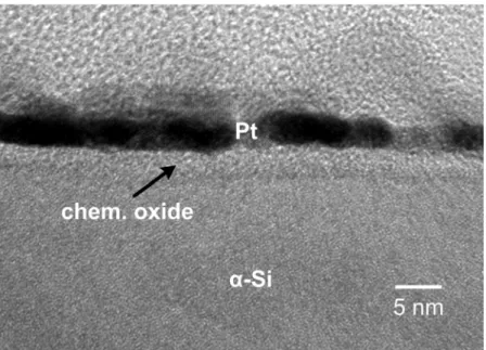
The transmission electronic microscopy (TEM) cross-section image of chemical oxide
layer was shown in Fig. 2-2. To examine the quality of chem-SiO2, after the chem-SiO2 layer
was formed, platinum was deposited on top of the chem-SiO2 for image contrast in TEM
sample preparation. A relation of chemical oxide thickness versus immersed time was also
investigated by TEM. As shown in Fig. 2-3, the chemical oxide growth controlled by
diffusion of reactants through the pre-existing layer conformed to the model of oxide growth.
The growth kinetic could be well represented with the expression (1) for the short time:
d = E ln ( 1 + Ft ) (1)
where E and F are adjusted parameters proportional to the penetration depth of the species and
to the concentration of the precursors, respectively [57]. In this work, there is an
approximately saturation thickness of 3.4 nm after dipped for 10 min. For this reason, it is
easy to achieve the same result when samples immersed into a chemical solution of 3H2SO4 :
1H2O2 over 10 or 15 min. For purposed comparison, the stable parameter at 20 min of
Fig. 2-3 Formation thickness of chemical oxide layer versus immersed time.
Fig. 2-2 TEM cross-section image of chemical oxide layer after dipped for 20 min. Platinum film deposited on the top of the chem-SiO2 layer was for the TEM sample preparation.
Figure 2-4 shows X-ray photoelectron spectroscopy (XPS) of Si2p peak for the chemical
oxide on top of α-Si layer with 20 min dipping. Black line is the raw data and the other lines
were obtained by the curve-fitting calculation. According to the detailed XPS studies of
surface oxidation layer of Si, it was observed Si, SiO and SiO2 peaks are located at binding
energy of 99.6, 101.7 and 103.2 eV, respectively [58]-[60]. We believe that the signal of Si
peak was obtained from the bottom layer (α-Si) because the thickness of chemical oxide layer
is less than XPS sampling depth. Therefore, it can be clear to define that the chemical oxide is
composed of SiO and SiO2.
Fig. 2-4 X-ray photoelectron spectroscopy (XPS) of Si2p peak for the chemical oxide on
2.3.2 Reduction of Ni concentration in MIC poly-Si films
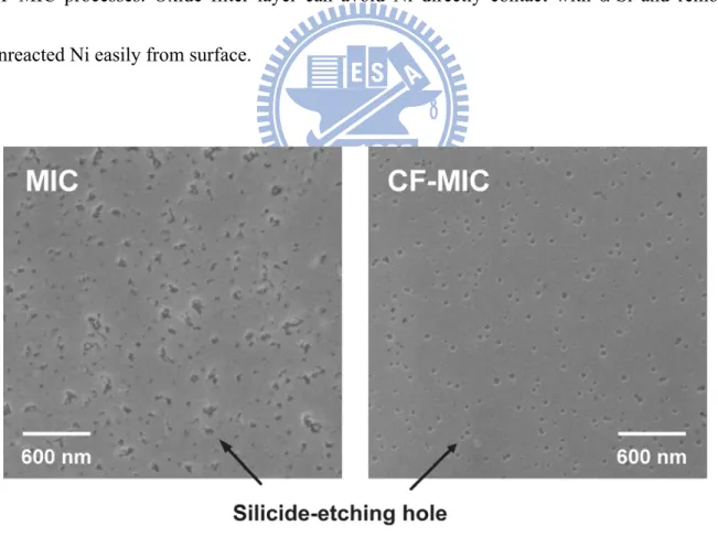
To investigate the effect of chemical oxide on the reduction of Ni residues, samples were
purposely dipped into a silicide-etching solution (HNO3:NH4F:H2O = 4:1:50) after unreacted
Ni film and chemical oxide layer were removed. As shown in Fig. 2-5, numerous holes were
observed. These holes were residues of Ni silicides that had been etched away by the
silicide-etching solution. The Ni residues in CF-MIC were much lower than those in
conventional MIC. This reduction must be due to the introduction of chemical oxide layer in
CF-MIC processes. Oxide filter layer can avoid Ni directly contact with α-Si and remove
unreacted Ni easily from surface.
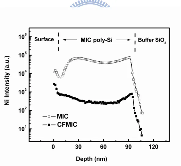
Secondary-ion mass spectroscopy (SIMS) depth profile was also used to analyze the Ni
concentrations (residues) in Si films (without silicide-etching process). As expected, Ni
content in CF-MIC was much less than that in MIC as shown in Fig. 2-6. Obviously,
chemical oxide layer can reduce the Ni concentrations in Si films. This is because the
diffusivity of Ni in α-Si is 108 times higher than that in SiO
2 at 500oC [61]-[62]. As a result,
chemical oxide serves as a filter, which can retard the in-diffusion of Ni into Si films. In
other words, Ni concentrations in Si films were reduced.
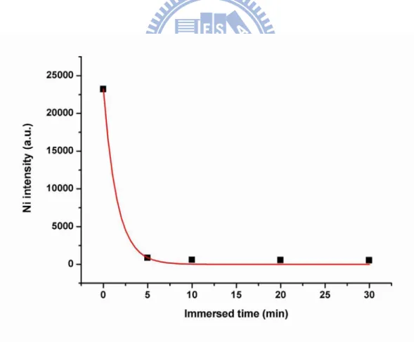
Moreover, to investigate the Ni reduction in various thicknesses of chemical oxide layer,
a relation of Ni intensity at a depth of 50 nm versus immersed time after MIC process is
shown in Fig. 2-7. It conformed to the basic diffusion model to presented exponential decay
as a function of immersed time and saturated at a minimum of Ni intensity after dipped for 10
min. The result indicated that the chemical oxide introduced between α-Si layer and Ni layer
can greatly reduced Ni concentration in MIC TFTs depended on thickness of the chemical
oxide. Hence the leakage current was improved to an optimum with the reduction of Ni
concentration because of increased thickness of chemical oxide.
Fig. 2-7 A relation of Ni intensity at a depth of 50 nm versus immersed time by SIMS after MIC annealing.
2.3.3 Surface roughness of MIC poly-Si films after crystallization
After Ni film and chemical oxidewere removed, their surfaces (without silicide-etching)
were measured using atomic force microscopy (AFM) to identify the degree of texturing. As
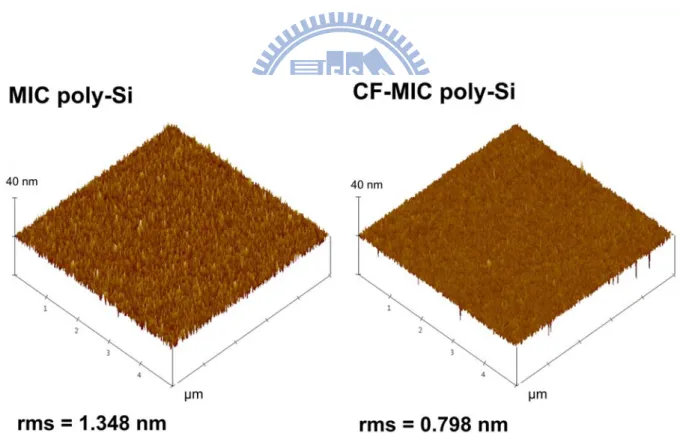
shown in Fig. 2-8, the root mean square surface (rms) roughness of CF-MIC surface (0.798
nm) was less than that of CF-MIC surface (1.348 nm). These results are in agreement with
the MICC studies of Choi et al. [56], who found that MIC with cap layer can achieve a clean
and smooth surface.
2.3.4 Electrical performance of MIC and CF-MIC TFTs
Figure 2-9 exhibits the ID–VG transfer characteristics of TFTs at a drain bias of 5 V. The
device parameters were extracted at W/L = 10/10 μm, and ten TFTs were measured. The
average values with standard deviations in parentheses were shown in Table 2-1. The
threshold voltage (Vth) is defined at a normalized drain current of IDS = (W/L) × 100nA at VDS
= 5V. The field-effect mobility (µFE) is extracted from the maximum value of
transconductance at VDS = 0.1V. As shown in Table 2-1, the electrical characters of CF-MIC
TFTs were significantly improved. This improvement must be due to the introduction of
chemical oxide layer in CF-MIC processes. Compared with conventional MIC TFTs, CF-MIC
TFTs shows a 17.3-fold increase in the on/off current ratio and a 14.3-fold decrease in the
Fig. 2-9 Typical IDS-VGS transfer characteristics and filed-effect mobility of of MIC, CF-MIC
and SPC TFTs (W / L = 10 / 10 μm)
Table 2-1 Average device characteristics of MIC, CF-MIC and SPC TFTs with standard deviations in parentheses
The leakage current improvement was attributed to the reduction of Ni concentration in
the CF-MIC films. It is known that Ni-related defects might degrade electric performance
because the trap states introduced dangling bonds and strain bonds [63]. The chemical oxide
layer reduced content of Ni (Ni-related defect) into channel layer during MIC annealing
process. With the reduction of the Ni concentration, the minimum leakage current was
reduced and therefore the on/off current ratio was increased [64]-[65]. In addition, the carrier
mobility also increased due to lower impurity scattering of Ni-related defects and grain
boundaries. However, the Vth of CF-MIC was showed a positive shift compared with
conventional MIC. The result is similar to earlier findings suggesting that the negative shift of
Vth was caused by positive charge in high Ni residues poly-Si film [54].
The electrical performances of SPC TFTs were also measured. As shown in Table 2-1,
Fig. 2-9, the on/off current ratio of CF-MIC TFTs was higher than that of SPC TFTs. The
leakage current of CF-MIC TFTs was as low that of SPC TFTs. This also demonstrated the
reduction of Ni residues through the introduction of chemical oxide layer.
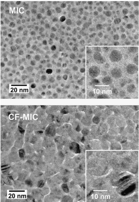
2.3.5 Influence of grain size on field-effect mobility
In general, the grains of MIC were crystallized from top to down and formed needle-like
approximately 8~10 nm and 15~18 nm, respectively. The variation of grain size was
attributed to the different Ni concentration during MIC annealing process [67]. The amount of
nucleation site of NiSi2 in MIC is higher than that in CF-MIC due to higher Ni concentration.
Therefore, the grain size of MIC was less than that of CF-MIC.
In the MIC poly-Si films, dangling bonds in grain boundaries serve as the trapping
centers, which trap many free carriers (either electrons or holes) and consequently hinder
carriers from conduction [33]-[35]. For this reason, the field-effect mobility increased from
Fig. 2-10 The plane-view images of transmission electronic microscopy (TEM) of MIC and CF-MIC poly-Si films.
2.4 Summary
The chemical oxide filter layer was introduced into MIC processes to reduce the leakage
current of MIC TFTs. The process was very simple and without extra expensive instrument. It
just added α-Si coated sample into chemical solution before depositing the Ni film. The
chemical oxide growth controlled by diffusion of reactants through the pre-existing layer
conformed to the model of oxide growth and there is a saturation thickness of 3.4 nm after
dipped for 10 min. It was also found that it conformed to the basic diffusion model to
presented exponential decay as a function of immersed time and saturated at a minimum of Ni
concentration after dipped for 10 min.
As the results, the electrical performance of MIC TFTs with chemical oxide layer was
significantly improved, including in higher field-effect mobility, superior subthreshold slope,
and higher on/off current ratio. Compared with conventional MIC TFTs, CF-MIC TFTs
shows a 14.3-fold decrease in the minimum leakage current and a 17.3-fold increase in the
on/off current ratio. This is because the chemical oxide layer can avoid Ni directly contact
with α-Si, avoid excess of Ni atoms into α-Si layer and remove unreacted Ni easily from
Chapter 3
Effect of Nickel Concentration on Electrical
Characteristics of MIC TFTs: Source/Drain Series
Resistance, Bias Reliability and Thermal Stability
3.1 Introduction
In recent years, low-temperature polycrystalline silicon (LTPS) thin-film transistors
(TFTs) have been widely applied to high resolution integrated active-matrix organic
light-emitting diodes (AMOLED), which exhibit good electrical properties and can be used in
the realization of glass substrate [48]. In various fabrication for LTPS, metal-induced
crystallization (MIC) is promising for use owing to its low cost, good uniformity, low
crystallization temperature (~500 ) and short crystallization time (0.5 ℃ - 5 h) [50]-[51].
Unfortunately, Ni and NiSi2 residues in the poly-Si film increases the leakage current and
shifts the threshold voltage [52]-[53]. In chapter 2, the leakage current has been significantly
reduced by decreasing the Ni concentration through use of a chemical oxide filter layer
(CF-MIC).
Noteworthily, while most studies have focused only on reducing Ni contamination to
series resistance of MIC TFTs. Inevitably, the S/D series resistance negatively influences on
the device performance, especially on-state current and mobility [68]-[70]. This phenomenon
becomes seriously due to increased ratio of the S/D series resistance at short channel devices.
Therefore, improving the performance of MIC TFTs requires understanding in detail how the
Ni concentration affects S/D series resistance. However, to our knowledge, exactly how Ni
concentration and series resistance are related at the S/D region has not been examined. In the
part 1, the S/D series resistance of MIC TFTs was investigated by using transmission line
method [69].
Moreover, bias reliability and thermal stability became major concerns for AMOLED
display applications, especially when devices are operated under hot carrier condition and
high temperature environment. It is known that hot carrier stress under high gate and high
drain voltages decreases on-state current and increases the threshold voltage (Vth) [71]-[72].
Furthermore, devices in high temperature environment show a poor thermal stability leading
to large leakage current and shifts Vth [73]-[74]. Although reducing Ni concentration is an
effective way to improve leakage current, the Ni concentration effect on bias reliability and
thermal stability was also important for AMOLED display application. It is interesting how
the reduction of Ni concentration affect the bias reliability and thermal stability of MIC TFTs.
In the part 2, the effect of Ni concentration on bias reliability and thermal stability were
In this study, exactly how the Ni concentration affects these electrical characteristics of
MIC TFTs is examined by using the conventional MIC and CF-MIC to represent high and
low Ni concentration devices, respectively. Results of this study demonstrate that the S/D
series resistance and channel resistance were decreased with the reduction of Ni concentration
in MIC poly-Si. It was also found that reducing Ni concentration in MIC films was also
beneficial for bias reliability and thermal stability.
3.2 Experimental procedure
Two kinds of MIC TFTs were investigated in this study, which were fabricated by using
the method in chapter 2. One is “MIC” fabricated by conventional nickel-induced
crystallization with high Ni concentration, and the other is “CF-MIC” fabricated by
metal-induced crystallization through a chemical oxide layer with low Ni concentration. After
the devices fabrication, transfer characteristics of TFTs were measured at room temperature
by using KEITHLEY 4200 semiconductor parameter analyzer.
3.2.1 Transmission line method (TLM)
In the part 1, the source/drain (S/D) series resistance of TFTs was extracted by using
transmission line method (TLM). In general, the TLM method is used to determine the series
to measure the series resistance of a top-gate TFT devices used to induce electrons into the
channel. The extraction of S/D series resistance in these gated structures differs slightly from
that of conventional TLM method since the measurement is performed at various gate
voltages. The method is commonly used to determine the series resistance between the source
and the drain of a transistor. It is comprised of the source resistance (RS), the channel
resistance (RCH) and also the drain resistance (RD). The total series resistance (RS/D) is the sum
of the resistance seen by RS and RD; RS/D = RS + RD. As shown in Fig. 3-1, S/D series
resistances are more complex in that they also include spreading resistance from the probe to
the channel and sheet resistance from the contact electrodes.
3.2.2 Hot carriers stress and thermal stress
In the part 2, the stressing voltage is setting at saturation region of on-state. Early studies
have demonstrated that the degradation of device increased with stress voltage from 20 V to Fig. 3-1 Schematic diagrams of an intrinsic transistor with a lumped parameter representation of the S/D series resistance [75].
30 V. In this case, the stress voltage was set at VDS = 20 V and VGS = 20 V for 7500 s
[76]-[78]. In general, hot carriers are particles that attain a very high kinetic energy from
being accelerated by a high electric field. These energetic carriers can be injected into
normally forbidden regions of the device, as the gate dielectric, where they can get trapped or
cause interface states to be generated. These defects then lead to threshold voltage shifts and
on-state current degradation of TFT devices. Moreover, thermal stability was examined at
elevated temperatures from 25 to 125°C. It is easy to the raise off-state curves with increase
of operation temperature due to mechanism of thermionic field emission [79].
3.3 Results and discussion
3.3.1 Effects of Ni concentration on source/drain series resistance
The transmission line method was employed to investigate the S/D series resistance
(RS/D), which is a standard approach for the extraction of the RS/D by fitting the ON-resistance
(RON) as a function of the channel length. In the linear region of the TFT output
characteristics (low drain voltage and high gate voltage), RON is assumed to consist of channel
resistance (RCH) and RS/D. The ON-resistance can be estimated as the following equations:
RON = (∂ VD/ ∂ID) = RCH + RS/D, RCH = L / [W µox Ci (VG-Vt)]
where Ci is the gate oxide capacitance per unit area and W, L, and Vt are the device channel
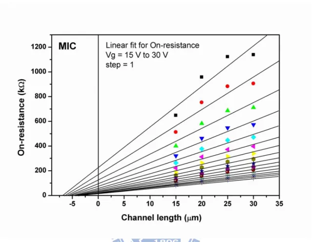
Figure 3-2 and figure 3-3 show the ON-resistance data of MIC TFTs and CF-MIC TFTs
as a function of the channel length, respectively. The ON-resistance of TFTs were evaluated
at VD = 0.1 V of the TFT output characteristics. Notably, the transistors have a fixed channel
width of 20 μm. The results showed that the ON-resistance increased with the increase of
device channel length; a large ON-resistance in the high Ni concentration device (MIC TFTs)
was also observed. By the linear fitting for different gate voltages, the interception with the
y-axis indicated the S/D series resistance of TFTs. Figure 3-4 shows the extracted S/D series
resistance and channel resistance as a function of the gate voltage. As the results, the S/D
series resistance and channel resistance of CF-MIC TFTs were lower than those of the
Fig. 3-2 Measured On-resistance of conventional MIC TFTs as a function of channel length.
Fig. 3-3 Measured On-resistance of CF-MIC TFTs as a function of channel length. The
In the S/D region, the device with a high Ni concentration (MIC TFTs) exhibited a
larger S/D series resistance than that of CF-MIC TFTs. Notably, the S/D series resistance can
be affected by crystalline quality and dopant concentration in the S/D region. First, in terms of
crystalline quality, samples were annealed at 600°C for dopant activation and
re-crystallization after ion implantation because the poly-Si in S/D region was amorphized by
a heavily doped implantation at a dosage of 5 × 1015 cm-2 [80]. Figure 3-5 shows the Raman
spectra of undoped and heavily doped poly-Si films after dopant activation at 600°C for 24 h. Fig. 3-4 The extracted S/D series resistance and channel resistance as a function of the gate
This figure reveals a poly-Si peak at 520 cm-1. Meanwhile, no a-Si peak appears at 480 cm-1,
indicating that all samples are transferred to polycrystalline structure. The heavily doped
poly-Si films show a lower Raman spectra intensity since re-crystallization of a-Si with Ni at
600°C is not oriented and growth is limited by formation of solid-state crystallization (SPC),
subsequently lowering crystallinity in the S/D region, as shown in Fig. 3-6. Furthermore, the
crystallinity of “CF-MIC + SPC” is superior to that of “MIC + SPC” because the less
nucleation site of NiSi2 causes a larger grain size in CF-MIC poly-Si films with a low Ni
concentration [67]. However, the crystallinity of S/D region is not different in a general
re-crystallization without Ni due to the only SPC mechanism. Second, the variation in S/D
series resistance can also be attributed to the dopant concentration. As is well known, heavily
doped implantation can significantly decrease the resistance of Si films. Unfortunately, Ni
atoms serve as acceptor-like dopants in silicon [81], which counteract the effects of
phosphorous doping and ultimately reduce the donor concentration in the S/D region. For this
reason, high Ni concentration decreases the conductivity of the S/D region, leading to large
S/D series resistance in MIC TFTs. As mentioned earlier, CF-MIC has a lower S/D series
Moreover, in the channel region, MIC TFTs also shows a larger channel resistance (RCH)
due to the high trap-state density and impurity scattering (Ni-related defects). According to
Fig. 3-5, CF-MIC presents a better crystalline quality than that of MIC at channel region.
Figure 3-7 shows the effective trap state density (Nt) uses Levinson and Proano’s method,
which can estimate the Nt from the slope of the linear segment of ln [ID / (VG-VFB)] vs. 1 /
(VG-VFB)2 at low VD and high VG, where VFB is defined as the gate voltage that yields the
Fig. 3-5 Raman spectra of undoped and heavily doped MIC poly-Si films after dopant
minimum drain current at VD = 0.1 V [82]-[83].Notably, the Nt of CF-MIC TFTs is 4.65×10¹²
cm-2, smaller than that of MIC TFTs (6.08×1012 cm-2). The results imply that the defects are
minimized in CF-MIC TFTs due to the reduced Ni concentration. As mentioned earlier, the
Ni atoms are obstructers for performance and S/D conductivity of the MIC TFTs. These
results verified that it is an efficient means to improve the electrical characteristics of a
channel and S/D region by reducing the Ni concentration in MIC TFTs.
Fig. 3-6 Schematic diagrams of MIC growth at at 500°C and SPC retard MIC growth at
![Fig. 1-2 The formation temperature map of thin-film Ni silicides on (a) α-Si, and (b) c-Si [31].](https://thumb-ap.123doks.com/thumbv2/9libinfo/8150486.167072/28.892.158.780.115.426/fig-formation-temperature-map-film-ni-silicides-si.webp)
![Fig. 1- 5 Schematic representation of band structure for inhomogenous-film model [33]](https://thumb-ap.123doks.com/thumbv2/9libinfo/8150486.167072/31.892.181.739.299.706/fig-schematic-representation-band-structure-inhomogenous-film-model.webp)