國 立 交 通 大 學
電機學院微電子奈米科技產業研發碩士班
碩士論文
以離子植入矽化物技術製作在矽化鎳與矽介面處低溫
摻雜活化的相關研究
Research of Low Temperature Dopant Activation at
Nickel Silicide and Silicon interface Using Implant Into
Silicide
研 究 生:林勝軍 Student:Sheng-Chun Lin
指導教授:張國明 博士 Advisor:Dr. Kow-Ming Chang
以離子植入矽化物技術製作在矽化鎳與矽介面處低溫
摻雜活化的相關研究
Research of Low Temperature Dopant Activation at
Nickel Silicide and Silicon interface Using Implant Into
Silicide
研 究 生:林勝軍 Student:Sheng-Chun Lin
指導教授:張國明 博士 Advisor:Dr. Kow-Ming Chang
國 立 交 通 大 學
電機學院微電子奈米科技產業研發碩士班
碩 士 論 文
A Thesis
Submitted to College of Electrical and Computer Engineering National Chiao Tung University
in partial Fulfillment of the Requirements for the Degree of
Master in
Industrial Technology R & D Master Program on Microelectronics and Nano Sciences
January 2008,
Hsinchu, Taiwan, Republic of China
以離子植入矽化物技術製作在矽化鎳與矽介面處低溫
摻雜活化的相關研究
研究生:林 勝 軍 指導教授:張 國 明 博士 國立交通大學電機學院產業研發碩士班摘要
金屬氧化半導體元件持續微縮至奈米等級時,將會使得源極、閘極和汲極的寄生 阻抗變大。因此,為了降低寄生阻抗和改善元件的性能,金屬矽化物的技術被發 展在深次微米的應用上。在奈米金屬氧化半場效電晶體的製造中,矽化製程是必 須的,為了抑制源極及汲極的超淺接面形成所產生的短通道效應。在本論文中, 對於先進元件的製造上,淺接面的形成和熱預算的控制是很重要的。我們結合了 離子植入矽化物技術製造和固態磊晶再成長的觀念去達成這兩個需求。對於金屬 和矽接面的二階段金屬快速退火60秒而言,磷離子植入的試片顯現出會比硼離子 植入更像是歐姆接觸。基於固態磊晶再成長摻雜物推積在介面處和離子植入矽化 物技術,我們的實驗將可以達到高劑量的活化和使用低溫退火,並且結合了電流 電壓和電容電壓量測法來了解固態磊晶再成長的行為。在固態磊晶再成長製程完 成之後,N基底和P基底的試片隨著較高的溫度預算400℃和500℃有可能會引起 缺陷的形成和摻雜物的反活化現象發生。 iResearch of Low Temperature Dopant Activation at Nickel
Silicide and Silicon interface Using Implant Into Silicide
Student: Sheng-Chun Lin Advisor:Dr. Kow-Ming Chang
Industrial Technology R & D Master Program of Electrical and Computer Engineering College
National Chiao Tung University
Abstract
With the continuing scaling-down to nanometer regime of metal- oxide-semiconductor (MOS) device will increase parasitic resistance of gate, source and drain. As a result, metal silicide has been developed used in deep submicron application for reducing the parasitic resistance and to improve device performance. In nanometer MOSFET fabrication, this silicidation process requires considering to suppress short channel effect (SCE) when forming the ultra shallow source and drain junction. In this thesis, Sallow junction formation and low thermal budget control are important for advanced device manufacturing. We combined the concept of implant into silicide (IIS) and solid phase epitaxial regrowth (SPER) to achieve both requirements. For M/S junction with 2nd RTA 60s, P+ implantation samples shows more like ohmic contact behaviors than BF2+
implantation samples. Based on the IIS dopant segregation pile-up at interface and SPER, our experiment would achieve the high dosage activation and using low temperature annealing, and combine the I-V and C-V measurement to know SPER behavior. After SPER process finished,
samples may cause defect formation and dopant deactivation phenomenon with higher thermal budget treatment above 450℃ for
N-sub and 500℃ for P-sub.
誌 謝
隨著碩士論文完成之際,回想在交大這兩年來的學習中,首先感 謝指導教授張國明教授的開明管教方式和諄諄教誨讓我們的研究生 涯受益良多,老師的鼓勵和關懷下,讓我們更快的融入實驗室的好環 境和氣氛,且在實驗室的豐富資源下學習和成長,不但學習到研究學 問的態度和方法,也學到待人接物的道理。謝謝老師。 同時也要感謝博士班學長、同學及學弟的教導與幫忙。另外特別 感謝一直指導我的林建宏學長,不論是在實驗、論文,及準備口試上 提供的建議及指導,讓我能順利的進行且完成。還有感謝交大奈米中 心、國家奈米實驗室提供著優良的環境和各種實驗設備,尤其是林聖 欽先生的協助。 最後要感謝我的父母,林榮森先生與陳春香女士,謝謝他們從小 到大對我的養育之恩以及教導我待人處世的道理,也要感謝賴淑惠小 姐陪伴我這兩年時間且給予的支持,沒有你們的支持與鼓勵我也沒辦 法順利完成碩士學位。Contents Chinese Abstract---i English Abstract---ii Acknowledgements--- iv Contents---v Table Captions---viii Figure Captions---xi Chapter 1 Introduction 1.1 General background---01
1.1.1 Silicide process technology---02
1.1.2 TiSi2 process---03
1.1.3 CoSi2 process---04
1.1.4 NiSi process---05
1.1.5 Implant into silicide (IIS)---06
1.1.6 Solid phase epitaxial regrowth (SPER)--- ---07
1.2 Motivation---08
1.3 Organization of thesis---09
1.4 References---10
Chapter 2 Formation of NiSi/p+n, NiSi / n+p Shallow Junction and NiSi/p+p, NiSi/n+n Metal-Semiconductor (MS) Junction 2.1 Introduction---13
2.2 Experimental procedures---16
2.3 Reference---17
Chapter 3 Electrical Characteristics and Physical Properties of NiSi/p+p, NiSi/n+n Metal- Semiconductor (MS) Junction Using Implant Into Silicide. 3.1 Surface morphology by AFM inspection ---21
3.2 Electrical measurements ---22
3.2.1 I-V measurements---22
3.2.2 Reverse leakage current density---24
3.2.3 Current-Temperature measurement---25
3.2.4 C-V measurements---25
3.3 References---26
Chapter 4 Electrical Characteristics of NiSi/n+p, NiSi/p+n ultra shallow Junction Using Implant Into Silicide. 4.1 C-V measurement---28
4.1.1 C-V measurement introduction---28
4.1.2 Results and discussion of C-V---30
4.2 I-V measurement---31
4.2.1 I-V measurement introduction---31
4.2.2 Results and discussion of I-V---32
4.3 Activation energy measurement---34
Chapter 5 Conclusion and Future Work ---36
Table Captions
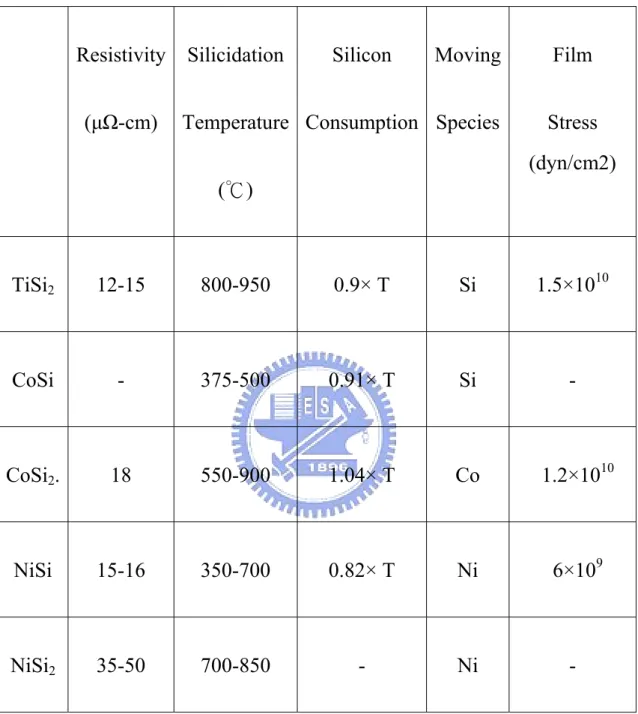
Table 1.1 Comparison the characteristics of Ti, Co and Ni silicides. ---39
Table 2.1 Process recipe of P+P, N+/N and P+N and N+/P junction by IIS
scheme. ---45
Table 2.2 Process recipe of P+P, N+/N and P+N and N+/P junction at
Figure Captions
Fig.1.1 Continuation of Moor’s Law from intel’s high-k/metal gate
announcement (2003). ---38
Fig.1.2 Schematic of issue associated with silicide process. ---38
Fig. 1.3 With/without bridging phenomenon of metal silicides. ---40
Fig. 1.4 Standard deviation of sheet resistance vs silicidation temperature.
---41
Fig. 2.1 Process flow of P+P, N+/N and P+N and N+/P junction samples of
silicide contact for I-V and C-V electrical properties measurement. ---45
Fig. 3.1 AFM image shows NiSi/Si interface morphology by 2nd RTP
annealing (a) 400 (b) 500 (c) 600 (d) 700 for 30 sec.℃ ℃ ℃ ℃
---47
Fig. 3.2 Four basic transport process under forward bias. ---48
Fig. 3.3 Depletion-type contacts to n-type substrates with increasing
doping concentrations. The electron flow is schematically indicated by the electrons and their arrows. ---48
Fig. 3.4 The forward ID-VD characteristic curves of the M/S junction
diode with 2nd RTA 30 sec by (a) BF2+ implantation and (b) P+
implantation. ---49
Fig. 3.5 The ID-VD characteristic curves of the M/S junction diode with
2nd RTA 60 sec by (a) BF2+ implantation and (b) P+ implantation.
---50
Fig. 3.6 The forward bias current density versus annealing temperature
for the NiSi / Si junction diodes fabricated with (a) BF2+ and (b)
P+ implantation at various annealing time. ---51
Fig. 3.7 The reverse bias current density versus annealing temperature for
the NiSi / Si junction diodes fabricated with (a) BF2+ and (b) P+
implantation at various annealing time. ---52
Fig. 3.8 The ID-VD characteristic curves of the M/S junction diode with
2nd RTA 60 sec by BF2+ implantation and measure temperature at
25, 45, 85 and 105℃, respectively. ---53
Fig. 3.9 The ID-VD characteristic curves of the M/S junction diode with
2nd RTA 60 sec by P+ implantation and measure temperature at 25, 45, 85 and 105℃, respectively. ---54
Fig. 3.10 The capacitance-voltage characteristics of Schottky junction
diodes implanted (a) BF2+ and (b) P+ without 2nd RTA. ---55
Fig. 4.1 Abrupt p-n junction in thermal equilibrium. (a) Space-charge
distribution. Dashed lines indicate corrections to depletion approximation. (b) Electric-field distribution. (c)Potential distribution where Vbi(Ψbi) is the built-in potential. (d)
energy-band diagram. ---56
Fig. 4.2 A 1/C2-V plot can yield the built-in potential and doping density.
---57
Fig. 4.3 Actually measure 1/C2-V plot. ---57
Fig. 4.4 Ψbi (a)N-sub samples (b)P-sub samples. ---58
Fig. 4.5 The dopant activation density of IIS at MS interface (a)Boron
doping density for N-sub samples (b)Phosphorous doping density for P-sub samples. ---59
becomes deeper away from M/S interface with 2nd RTA temperature. ---60
Fig. 4.7 ideal factor (a)N-sub samples (b)P-sub samples. ---61
Fig. 4.8 Ion - Ioff relation graphics (a)N-sub samples (b)P-sub samples
(Ion: Forward bias at 1V and Ioff: Reverse bias at 2V). ---62
Fig. 4.9 The reverse current density curves of the P/N junction diode with
2nd RTA 60 sec by (a) BF2+ implantation (b) P+ implantation. ---63
Fig. 4.10 Compare to the forward current density curves of the P/N
junction diode with 2nd RTA 60 sec by BF2+ implantation (a)
20keV/5E13cm-2 (b) 50keV/5E15cm-2. ---64
Fig. 4.11 Compare to the forward current density curves of the P/N
junction diode with 2nd RTA 60 sec by P+ implantation (a) 20keV/5E13cm-2 (b) 30keV/5E15cm-2. ---65
Fig. 4.12 Arrhenius plot for NiSi/Si interface (a) P+N junction fabricated
by BF2+ implantation. (b) N+P junction fabricated by P+
implantation. The measurement was conducted at 2V reverse bias. ---66
Fig. 4.13 The activation energy of NiSi/Si interface (a) P+N junction
fabricated by BF2+ implantation. (b) N+P junction fabricated
by P+ implantation. ---67
Chapter 1
Introduction
1.1 General background
With the continuing scaling-down to nanometer regime of metal- oxide-semiconductor (MOS) device, resulting in large packing density and increased complexity on the chip. Hence, the line width of interconnects becomes narrower and thus increases the interconnect resistance. Complementary metal-oxide- semiconductor (CMOS) device with gate length down to 0.1um will increase parasitic resistance of gate, source and drain, resulting in a lower switching speed and more power consumption. Therefore, the parasitic resistance between the metal and the source/drain becomes significant relative to other resistance in the circuit. Metal silicide has been widely used in deep submicron application for reducing the parasitic resistance and to improve device performance.
According to the 45nm CMOS technology node of Intel’s high-k/metal gate announcement, as shown in Fig. 1.1, gate dielectric and gate electrode are using high-k and metal material, respectively. In this thesis, we employ characteristic of metal silicide to form shallow junction which combined the concept of implant into silicide (IIS) and solid phase epitaxial regrowth (SPER). Future generations of CMOS technology have very strong requirements for junction activation level, abruptness, and depth control [1].
In other words, shallow junction formation is important beyond the 45nm CMOS node.
1.1.1 Silicide process technology
Metal silicide are often used on source/drain junction, gate and local interconnects to reduce the series resistance of the device, lead to higher switching speed for the device [2-3]. silicide is formed by solid-state reaction between a metal and Si. The metal-Si reaction is much faster than the metal–SiO2 reaction. Hence, the silicide formation is a self-aligned
process because of silicide forms merely in regions where Si is exposed. As a result, silicide technology is compatible with conventional CMOS process since no extra mask is needed in the self-aligned process. Before metal deposition to minimize the amount of native oxide because the solid-state reaction is very sensitive to impurities such as oxygen at the metal-Si interface or in the metal itself [4]. It has to be concerned about thermal process environment. Annealing must be done in a furnace with a low background concentration of oxygen to ensure that the metal does not oxidize during silicide formation. In actual, it is ensure to achieve low oxygen concentration in rapid thermal annealing (RTA) chamber than in furnace [5].
Silicides formation by solid state reaction often consumes contamination and defects at the original metal-Si interface, resulting in low contact resistance for ohmic contacts. Therefore, some critical drawbacks associated with the silicide process. Overly surface defect and contamination or doping can suppress silicide formed, resulting in higher sheet resistance and
non-uniform silicide thickness. During high temperature annealing will cause silicide prominent and junction leakage current. For silicides on polysilicon gates, grain growth in the polysilicon can occur resulting in threshold voltage shifts or gate oxide leakage. Those issue as shown in Fig. 1.2.
Recently, many silicide have been discussed to use to improve device performance, such as PtSi2, TiSi2, CoSi2, MoSi2, WSi2 and NiSi and so on.
Some of the silicide such as TiSi2, CoSi2 and NiSi is widely used in
integrated circuit (IC) process. Compare the characteristic between Ti, Co and Ni silicides as shown in Table 1.1. For TiSi2 and CoSi2 have low
resistivity and rather high thermal stability so that widely used in silicides application. Nowadays TiSi2 and CoSi2 can not become the trend because of
it has critical issue limit their development to future nanometer regime. Below, some unique properties and problems associated with the most common silicides are discussed.
1.1.2 TiSi2 process
There are two phase of TiSi2, corresponding to different crystal structures.
The C49 phase formed at first with high resistivity(60 – 300 μohm-cm) whereas the C54 phase with low resistivity(15 – 35 μohm-cm). However, we hope to obtain C54 phase with low resistivity. TiSi2 is generally formed
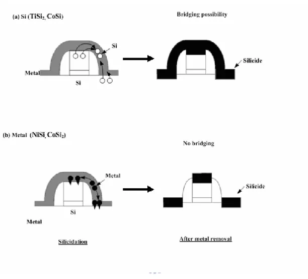
with a two-step annealing process because of Si is the dominant moving species during silicide formation, which results in excessive lateral silicide and bridging formed during over high the first annealing temperature. Another explained is that the conversion to the low resistivity phase of C54
is nucleation limited, requiring high thermal budget to ensure complete conversion [6].
TiSi2 has need two-step annealing to eliminate bridging effect (as show in
Fig. 1.3) and complete conversion to C54 phase. In addition, as the line width less than 0.2um, the sheet resistivity of TiSi2 increase with decrease
line width. Generally, the first annealing at 600 - 700℃ with nitrogen ambient result in formation phase of C49 of TiSi2. Nitrogen diffusion into
the Ti will form TiN/TiSi2 bi-layer rather than TiSi2 along. TiN would block
the lateral diffusion of Si which is used to prevent bridging. Then, second annealing is performed at a higher thermal budget to convert the TiSi2 to the
low resistance C54 phase. In addition, Ti is very effective reducing native oxides in contact, because of the high solubility of oxygen in Ti [7].
1.1.3 CoSi2 Process
Although the resistivity and thermal stability of CoSi2 similar to TiSi2.
Unlike TiSi2, the sheet resistivity of CoSi2 is insensitive to decrease line
width [8]. The CoSi2 is generally formed at first step which is a low
temperature anneal (400 - 500℃) to form the Co-rich silicide to reduce lateral silicide formation. Then a more high temperature anneal (600 - 800℃) to form CoSi2 with low resistivity.
Compared with the process windows of CoSi2 is less than the TiSi2 which
is a possible alternative to TiSi2 for silicide applications. However, high Si
consumption during the formation of CoSi2 silicide is a major drawback for
shallow junction. In addition, CoSi2 is sensitivity to interfacial oxide,
consequently generally capping a passivation layer to prevent oxidation [9-10]. When the device dimensions are scaled down and pattern density is increased it is important to minimize the stress induced by silicide formation because dislocations will be generated when the stress exceeds. Beside CoSi2 can be used as a diffusion source to form shallow junctions [11].
1.1.4 NiSi process
Recently there has been great interest in using NiSi for nanometer regime application. Ni-silicide has been identified as the best candidate for nanometer regime for main advantage are listed below: (1) low resistivity (15-16μΩ-cm), (2)low silicidation temperature (350-700 ℃ ), (3)low Si consumption (0.82× TNiSi), (4) Formation controlled by Ni diffusion, (5)
Low film stress (6×10⁹ dyn/cm2).
Nickel silicide has a low electrical resistivity which is comparable to those of TiSi2 and CoSi2. The sheet resistance of NiSi is relatively insensitive to
the line width of the silicide [12]. The NiSi has a lower formation temperature than TiSi2 and CoSi2. The conventional NiSi silicide usually
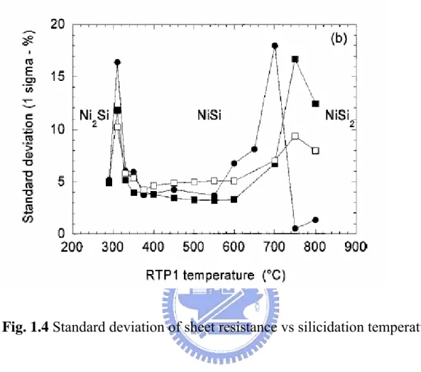
formed by one-step rapid thermal annealing (RTA) process. Hence, excess silicidation was found with one-step RTA NiSi leading to insensitive to line width of sheet resistance, increased diode leakage, and lower diode breakdown issues. To avoid excess silicidation formation was using to two-step RTA NiSi for CMOS applications. NiSi silicidation formed has three main regime, Ni2Si, NiSi and NiSi2 phase. The two peaks in the
transformation (as show in Fig. 1.4), respectively [13]. At temperature lower than 300 ℃ , Ni2Si formed which the resistance is higher. When the
annealing temperature between 300-400℃, the silicdie formed is Ni2Si or
mixture of Ni2Si/NiSi. The lower resistive NiSi is the stable phase for
temperatures ranging between 400 and 600℃. At temperature higher than 700℃, NiSi transform to NiSi2 phase with agglomeration which is two to
three time higher compared to the resistivity of NiSi phase. Therefore, NiSi has lower formation temperature than TiSi2 and CoSi2 with resistivity, which
compatible to High-k dielectric for future device fabrication.
NiSi has lower Si consumption than CoSi2 and TiSi2 that effective reduce
spiking shallow junction to obtain lower reverse bias leakage current. If dominant moving species is Si, the movement of Si atoms into metal film causing CMOS device fail, such as TiSi2. Moreover, Ni is the dominant
moving species during formation NiSi process, which effectively reduce the bridging phenomenon. Actual film stress can affect the electrical properties of device. NiSi has characteristic of lower film stress to reduce dislocations generated, junction leakage and gate oxide leakage.
1.1.5 Implant into silicide (IIS)
The implant into silicide (IIS) processes has been investigated for shallow junction formation. The IIS process consists of implanting dopants into silicide or metal layer and the subsequent thermal annealing to form a silicide-contacted shallow junction [14-17]. The IIS scheme in particular is of much benefit to the formation of shallow junction. This is because metal silicides have a larger nuclear stopping power than silicon for the implanted
dopant ions and thus can reduce the channeling effect; in addition, the junction formed by the IIS scheme can be almost free of implant damage, which is mostly confined in the silicide layer. And dopant segregation phenomenon can pile up the dopant concentration profile at the silicide/silicon interface after thermal annealing, it has a potential to form a better ohmic contact. Thus, the post-implant annealing temperature can be lowered while shallow junctions with superb characteristics can be obtained. Moreover, the silicided junction is conformal to the silicide/silicon interface, and thus the possibility of junction penetration by the silicide is reduced.
1.1.6 Solid phase epitaxial regrowth (SPER)
For high performance device applications, it is important to overcome the doping solid solubility limited by the conventional RTA at high temperature for reducing the resistance of source and drain. The use of low temperature solid phase epitaxial regrowth has been demonstrated in recent years as an alternative to the high temperature anneal method for junction formation. The SPER works on the principle that dopants in an amorphous Si region will activate to a level above the equilibrium solid solubility during crystalline regrowth. The SPER main advantages are the above equilibrium solid solubility dopants, good control junction depth, conventional high temperature was superseded and compatibility with high-k and metal gate thermal budget requirements. The main drawback of SPER is related to the relative high density of interstitial defect band at end-of-range (EOR) after the annealing, due to the relatively low thermal budget of the low temperature SPER anneal [18-20]. These EOR defects are not what we want, which result in increased junction leakage current.
1.2 Motivation
In the advanced integrated circuit technology, the channel length of MOSFET has been scaled down which require to reduce junction depth of source and drain minimize short channel effect. Into nanometer regime, the performance and electrical properties of CMOS will to support more difficulties. In next generation, high-k/metal gate stack technology is promising become to trend beyond the 45nm CMOS device, although it is need to be overcome more issue. The conventional junction of S/D required activation at high temperature annealing, but higher thermal budget will cause to affect the dopant concentration profile and the high-k dielectric crystallized. However, low temperature activation is required that formation ultra shallow junction for future CMOS technology. The formation shallow, abrupt, and activation junction is one of the main challenges for future minimize transistor dimension [21].
The Hf-base is possible alternative candidate for high-k dielectric in near term. The high-k dielectric will be crystallized at high temperature process, result in the gate leakage current increased. Since thermal reliability is playing an import role for high-k/metal gate stack, so we lead in NiSi to form metal gate material because of the NiSi has low and wide process windows. It is not only low process windows moreover would be to employ characteristic of NiSi to formation shallow and activation junction. In addition, the NiSi is a good diffusion source which the silicide as diffusion source (SADS) process has been proposed for the formation of silicide contacted shallow junction [22].
In parallel with the gate dielectric engineering to improve the thermal reliability of high-k dielectric, we are interesting in the project about low temperature activation. If the process temperature after gate dielectric formation can be lowered, the issue of high-k dielectric crystallized in process integration can also be minimized. We combined the concept of implant into silicide (IIS) and solid phase epitaxial regrowth (SPER) to control junction depth and junction activation. To make silicides with shallow junctions are to implant dopant through a deposited metal layer or silicided layer, called the implant into silicide. SPER works on the principle that dopants in an amorphous silicon region will activate to a level above the equilibrium solid solubility during crystalline regrowth.
These two methods lower the dopant activation temperature through the concept of change the surface energy of silicon and pile up the dopant concentration in NiSi/Si interface by dopant segregation and/or higher the solubility of the dopant in Si through the Si re-crystallization process. Details about these two methods with our experiment will be discussed in the following chapters.
1.3 Organization of the Thesis
In this thesis, we concentrate our efforts on the activation of B and P implant through silicide by RTA process. However, studies the fabrication and characterization of the NiSi contacted NiSi/p+n and NiSi/n+p shallow junction diodes and NiSi/n+n and NiSi/p+p ohmic contact formed by implant into silicide.
and the motivation of this thesis are mentioned.
In chapter 2, Formation of NiSi/p+n, NiSi/n+p Shallow Junction and NiSi/p+p, NiSi/n+n Metal-Semiconductor (MS) Junction.
In chapter 3, present Electrical Characteristics and Physical Properties of NiSi/p+p, NiSi/n+n Metal- Semiconductor (MS) Junction Using Implant Into Silicide.
In chapter 4, discuss Electrical Characteristics of NiSi/n+p, NiSi/p+n ultra shallow Junction Using Implant Into Silicide.
In chapter 5 is conclusions and future works.
1.4 References
[1] B. J. Pawl, R.Lindsay, R. Surdeanu, B. Dieu, L. Geenen, I. Hoflijk, O. Richard, R. Duffy, TClarysse, B. Brijs, W. Vandervorst, C. J. J. Dachs, J. Vac. Sci. Technol. B 22(1), Jan/Feb 2004, p.297-301.
[2] K. C. Saraswat and F. Mohammadi, IEEE Trans. Electron Devices, ED-29(1982) 645.
[3] D. B. Scott, W. R. Hunter and H. Shichijo, IEEE Trans. Electron Devices, ED-29(1982) 651.
[4] H. Berger and S. –Y. Lin, in S. Broydo and C. M. Osburn (eds.), ULSI Science and Technology, Vol. 87-11, Electrochemical Soc., Inc., Pennington, NJ, 1987, p.434.
[5] J. P Gambino, E. G. Colgan, Materials Chemistry and Physics 52 (1998) 99-146.
[6]. J. B. Lasky, J. S. Nakos, O. J. Cain and P. J. Geiss, IEDM Trans. Electron Devices, ED-3458 (1991) 262.
[7] T. B. Massalski (ed.), Binary Alloy Phase Diagrams, ASM International, Materials Park, OH, 1990.
[8] K.Maex, Mater. Sci. Eng. Rev., R11 (1993) 53.
[9] J. K. Kittl, Q. Z. Hong, H. Yang, N. Yu, S. B. Samavedam, and M. A. Gribelyuk, Thin Solid Films, 332, 404 (1998).
[10] K. Maex, A. Lauwers, P. Besser, E. Kondoh, M. de Potter, and A. Steegen, IEEE Trans. Electron Devices, ED-46, 1545 (1999).
[11] J. B. Lasky, J. S. Nakos, O. J. Cain and P. J. Geiss, IEDM Trans. Electron Devices, ED-3458 (1991) 262.
[12]T. Ohguro, S. Nakamura, E Morifuji, M. Ono, T. Yoshitomi, M. Saito, H. S. Momose and H. lwai Tech. Dig. Int. Electron Devices Meet. 1995, 453.
[13] A. Lauwers, A. Steegen, M.de Potter, R. Lindsay, A. Satta, H. Bender and K. Maex, J. Vac. Sci. Technol. B. B19, 2026 (2001).
[14] C.-Y. Lu, J. J. Sung, R. Liu, N.-S. Tsai, R. Sing, S. J. Hillenius, and H. C. Kirsch, IEEE Trans. Electron Devices 38, 246, (1991).
[15] Q. Wang, C. M. Osburn, C. A. Canovai, IEEE Trans. Electron Devices 39, 2486, (1992).
[16] R. Angelucci, S. Solmi, A. Armigliato, S. Guerri, M. Merli, A. Poggi, and R. Canteri, J. Appl. Phys. 69, 3962, (1991).
[17] B. S. Chen and M. C. Chen, IEEE Trans. Electron Devices 43, 258, (1996).
[18] R. Lindsay, S. Severi, B. J. Pawlak, K. Henson, A. Lauwers, X. Pages, A. Satta, R. Surdeanu, H. Lendzian, and K. Maex, IEEE 2004, p.70-75.
[19] S. Severi, B. J. Pawlak, R. Duffy, E. Augendre, K. Henson, R. Lindsay, and K. De Meyer, IEEE Electron Devices Letters, Vol. 28, NO. 3, March 2007, p.198-200.
[20] R. Duffy, M. Aboy, V. C. Venezia, L. Pelaz, S. Severi, B. J. Pawlak, P.eyben, T. Janssens, W. Vandervorst, J. Loo and F. Roozeboom, IEEE Trans. Electron Devices Vol. 53, NO. 1, January 2006, p.71-77.
[21] R. Lindsay, K. Henson, W. Vandervorst, and K. Maex, B. J. Pawlak, R. Duffy, R. Surdeanu, and P. Stolk, J. A. Kittl, S.Giangrandi, X.Pages and K. van der Jeugd, J. Vac. Sci. Technol. B 22(1), Jan/Feb 2004, p.306-311.
[22] C. C. Wang, C. J. Lin, M. C. Chen, Electrochemical Society, 150 (9) G557-G562 (2003).
Chapter 2
Formation of NiSi/p
+n, NiSi / n
+p Shallow Junction and
NiSi/p
+p, NiSi/n
+n Metal-Semiconductor (MS) Junction
2.1 Introduction
Conventional p-n junctions were formed by ion implantation dopant into Si substrate followed by high temperature furnace annealing for dopant activation and implantation damage annihilation. Therefore, channeling effect and high temperature dopant diffusion limit the formation of shallow junction. This is particularly important for the p+n junction because boron is a light element and diffuses fast in silicon. Consequently, low temperature activation technique is more important in nanometer regime. In recent years, many advanced junction formation techniques have been studied, such as, preamorphization [1, 2, 3], low energy implantation [4, 5], gas-immersion laser doping (GILD) [6, 7], decaborane (B4H10) implantation [8, 9], implant
into silicide (IIS) [13-16] and solid phase epitaxial regrowth (SPER) [17-21]. These new methods are briefly reviewed as follows:
(1) Pre-amorphization of silicon substrate before dopant implantation
Pre-amorphization has been widely used to control the channeling behavior of implanted dopant atoms. After the pre-amorphization of the silicon substrate surface layer, dopant implantation was performed followed
by crystal regrowth and annealing process for the junction formation. Many heavy atoms have been used as pre-amorphization species, such as Si and Ge. Solid phase epitaxial (SPE) scheme can be used to regrow the crystal from the amorphous layer at a temperature as low as 550 ℃. The growth rate depends on the element used for pre-amorphization as well as the dopant implanted following the pre-amorphization. A careful annealing process is needed to annihilate the massive defects and dislocation induced by the pre-amorphization.
(2) Low energy ion implantation
This is an extension of the conventional ion implantation technique. The implantation energy is lower than 1 keV and the implantation dose is typically from 1×10¹⁴ to 5×1014 cm-2. The major disadvantage of this method is that no commercial implantation system of such a low energy ion beam is available for high throughput mass production with reasonable cost.
(3) gas-immersion laser doping (GILD)
The gas immersion laser doping (GILD) process is a candidate technology for shallow junction formation. Gaseous dopant precursors (BCl3) are
chemisorbed on the silicon surface, and partially incorporated during the melting / recrystallisation of the Si top layer induced by an UV laser pulse (λ = 308 nm, pulse duration » 25 ns) [10]. The resulting thickness and dopant concentration of the doped layer depend on the laser energy density and the number of chemisorption / laser-induced incorporation cycles (up to 200). For the GILD technique both to eliminate the problems associated with ion implantation, and the unwanted diffusions that occur during the dopant activation anneals. Hence, GILD both have issues of Non-equilibrium phase
transformations and Strong dependence of recrystallized structure on the applied energy density.
(4) decaborane (B4H10) implantation
For CMOS scaling to nanometer region, particularly PMOSFET fabrication becomes more serious due to the difficulty of low energy boron ion implantation for source/drain (S/D). It can suppression of the boron diffusion which is caused by both transient enhanced diffusion (TED) and thermal diffusion (TD) that occur during the activation annealing. Therefore, implant boron atoms by conventional ion implantation is difficulty. Decaborane implantation technology has been proposed using boron cluster [11, 12]. The cluster contain n boron atoms, only one charge per cluster is required to accelerate n boron atoms. Clusters can be transported at relatively high energy for shallow junction, due to low impact energy per boron atom. Decaborane are contains 10 boron atoms where the energy per boron atom is about 1/11 that of the energy of the molecule. Therefore, decaborane technology can to achieve forms a shallow junction with a low temperature RTA to prevent thermal diffusion after deep S/D formation with a relatively high temperature RTA to maintain a high gate capacitance (Cgox)
and low contact resistance (Rc).
About above-mentioned methods, consideration high cost, massive defects and dislocation induced, high throughput mass production with reasonable cost and instrument and so on problems that make us inclined to use simpler, less damages and reach high dopant activation technology such as IIS and SPER. IIS and SPER technology were already discussed in chapter 1. Therefore, we conduct these two kinds of technology to formation
shallow junction in the experiment. IIS and SPER have played an important role while formation shallow junction in the future. IIS and SPER process potential advantages are more simples and effectively enhance activation than other method for formation of shallow junction. Briefly discuss advantages for IIS and SPER process. First, metal silicides have a larger nuclear stopping power than silicon for the implanted dopant and thus can reduce the channeling effect. Second, to formation shallow junction can greatly reduce ion implantation damages, due to ion implantation damages almost stay in the metal silicide. Third, silicides/silicon interface has thin amorphous silicon during silicidation process, in this time, we employ characteristic of SPER to raise dopant activation for shallow junction. In conventional process often make to pre-amorphous step which will increases more damages for shallow junction.
In this chapter, we investigate fabrication of NiSi/p+p, NiSi/n+n MS junction and NiSi/p+n, NiSi/n+p shallow junction. We would combine the dopant pile-up characteristic of IIS at interface and the ability of SPER to achieving the formation of shallow junction.
2.2 Experiment procedures
Samples were fabricated on p-type/n-type (100) oriented Si wafers. After a standard RCA clean process. Following, a 300 nm isolation oxide was grown on the wafer by wet oxidation at 1000℃ for 35 min. The active area regions were defined by the photolithography and etched by BOE (buffered oxide etchant) solution. Next, standard clean was used again to fully remove
the contamination. Following, a 200 Å Ni deposited on the wafer in a Dual E-gun Evaporation system with a base pressure of less than 2×10⁻⁶ torr, using a Ni target in vacuum ambient with a deposition rate of about 0.8- 1.2 Å/sec. After the Ni film deposition, the samples were rapid thermal annealed (RTA) at 400℃ for 30 sec in N2 ambient to form NiSi. The unreacted Ni
film was selectively etched using a solution of H2SO4 : H2O2 = 3 : 1 at
75~85℃ for 45 sec. Then, the sample of NiSi were implanted with BF2+/P+
ions at an energy of 20 to a dose of 5×1013 cm-2. We deposited Ti on NiSi with lift-off technology. Before samples were coated the Ti 50nm by Dual E-gun Evaporation system which used photolithography to define the four-point probe measuring pads, next to removed PR by ACE. Samples were deposited TaN 150nm by DC sputtering system on backside. Finally, followed by rapid thermal anneal (RTA) at 450 to 600℃for 60 sec in N2
ambient for the activation dopant, as shown in Fig. 2.1. Process recipe is listed in Table 2.1 and Table 2.2.
2.3 References
[1] M. C. Ozturk, J. J. Wortman, C. M. Osburn, A. Ajmera, G. A. Rozgonyi, E. Frey, W. –K. Chu, and C. Lee, IEEE Trans. Electron Devices Lett., vol. 35, p. 659, 1998.
[2] C. –M. Lin, A. J. Steckl, and T. P. Chow, IEEE Electron Device Letters, vol. 9, p. 594, 1998.
on Advanced MOS and Bi-Polar Devices, 1995.
[4] S. Talwar, G. Verma, and K. H. Weiner, 1998 International Conference on Ion Implantation Technology Proceedings, vol. 2, p. 1171, 1998.
[5] K. –I Goto, J. Matsuo, Y. Tada, T. Tanaka, Y. Momiyama, T. Sugii, and I. Yamada, 1997 Technical Digest. International Electron Devices Meeting, p. 471, 1997.
[6] P. G. Carey, K. H. Weiner, and Thomas W. Sigmon, IEEE Electron Device Letters, vol. 9, p.542, 1988.
[7] E. Ishida and L. Larson, University/Convernment/Industry Microelectronics Symposium, 1995. , Proceedings of the Eleventh Biennial, p. 105, 1995.
[8] M. A Foad, R. Webb, R. Smith E. Jones, A. Al-Bayati, M. Lee, V. Agrawal, S. Banerjee, J. Matsuo and I. Yamada, 1998 International Conference on Ion implantation Technology Proceedings, vol. 1, p. 106, 1998.
[9] K. Goto, J. Mastuo, T. Sugii, H. Minakata, I. Yamada, and T. Hisatsugu, 1996 International Electron Devices Meeting, p. 435, 1996.
[10] G. Kerrien, J. Boulmer, D. Débarre, D. Bouchier, A. Grouillet., D. Lenoble, Appl. Surf. Sci. 186 (2002) 45
[11] M. A. Foad, J. England, S. Moffatt, and D. G. Armour, Proc. 11th Inr. Conf On Ion Imp. Tech. -1996, IEEE, p.603,1997.
[12] K-I. Goto, J. Matsuo, T. Sugii, H. Minakata, I. Yamada, and T. Hisatsugu, Novel shallow junction technology using decaborane (B10H14)
IEDM Tech. Dig., pp.435-438, 1996.
[13] C.-Y. Lu, J. J. Sung, R. Liu, N.-S. Tsai, R. Sing, S. J. Hillenius, and H. C. Kirsch, IEEE Trans. Electron Devices 38, 246, (1991).
[14] Q. Wang, C. M. Osburn, C. A. Canovai, IEEE Trans. Electron Devices 39, 2486, (1992).
[15] R. Angelucci, S. Solmi, A. Armigliato, S. Guerri, M. Merli, A. Poggi, and R. Canteri, J. Appl. Phys. 69, 3962, (1991).
[16] B. S. Chen and M. C. Chen, IEEE Trans. Electron Devices 43, 258, (1996).
[17] B. J. Pawlak, R. Lindsay, R. Surdeanu, B.Dieu, L. Geenen, I. Hoflijk, and O. Richard, R. Duffy, T. Clarysse, B. Brijs, and W. Vandervorst, C. J. J. Dachs, J. Vac. Sci. Technol. B 22(1), Jan/Feb 2004, p.297-301.
[18] R. Lindsay, K. Henson, W. Vandervorst, and K. Maex, B. J. Pawlak, R. Duffy, R. Surdeanu, and P. Stolk, J. A. Kittl, S.Giangrandi, X.Pages and K. van der Jeugd, J. Vac. Sci. Technol. B 22(1), Jan/Feb 2004, p.306-311.
[19] R. Lindsay, S. Severi, B. J. Pawlak, K. Henson, A. Lauwers, X. Pages, A. Satta, R. Surdeanu, H. Lendzian, and K. Maex, IEEE 2004, p.70-75.
[20] S. Severi, B. J. Pawlak, R. Duffy, E. Augendre, K. Henson, R. Lindsay, and K. De Meyer, IEEE Electron Devices Letters, Vol. 28, NO. 3, March
2007, p.198-200.
[21] R. Duffy, M. Aboy, V. C. Venezia, L. Pelaz, S. Severi, B. J. Pawlak, P.eyben, T. Janssens, W. Vandervorst, J. Loo and F. Roozeboom, IEEE Trans. Electron Devices Vol. 53, NO. 1, January 2006, p.71-77.
Chapter 3
Electrical Characteristics and Physical Properties of NiSi/p
+p,
NiSi/n
+n Metal- Semiconductor (MS) Junction Using Implant
Into Silicide.
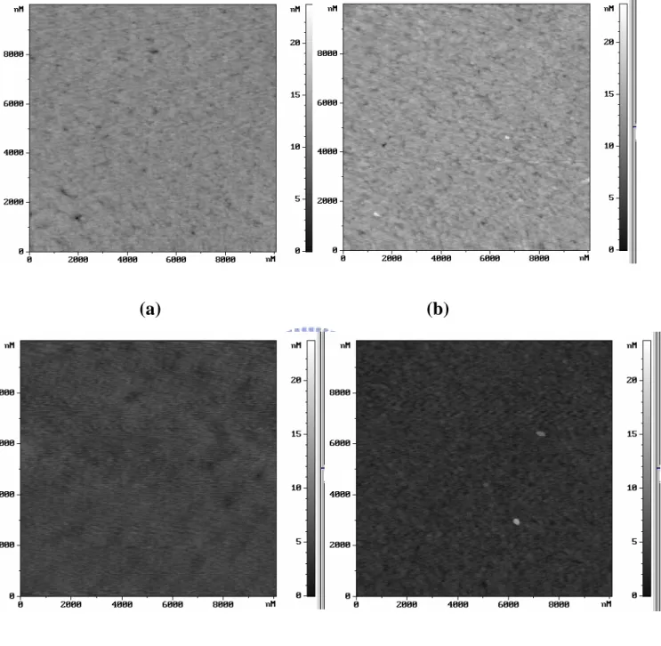
3.1 Surface morphology by AFM inspectionIn 1986, Binning et al. introduced another apparatus for surface characterization in atomic scale, the atomic force microscope (AFM). Since it can be applied to any types of material and environment, AFM has thus been used widely in surface characterization. Owing to its atomic scale resolution capability, AFM is also powerful equipment for nano-structure fabrication. We want to inspect the surface morphology of NiSi/ Si interface by AFM. Because of the roughness between the NiSi/ Si interface related to the junction leakage. We want to know the impact on roughness of temperature.
Fig. 3.1 AFM image shows NiSi/Si interface morphology by 2nd RTP annealing (a) 400℃ (b) 500℃ (c) 600℃ (d) 700℃ for 30 sec. Samples (n-type substrate, phosphorous doped) without 2nd RTA and with 2nd RTA 30sec at different temperatures (400, 500 ,600, and 700 ℃) are prepared. The AFM inspection results for these samples (Area: 10μm x 10μm), and all RMS values are around 1nm. For the 2nd annealing sample, the interface roughness at 700℃ 30sec is smoother than others sample. Therefore 2nd
annealing may improve interface roughness.
3.2 Electrical measurements
The electrical properties of the silicide-contacted shallow junction diodes fabricated by the IIS scheme are dependent on a number of factors, including the dopant activation level, implantation damage recovery, silicide/silicon interface roughness, and the distance between the silicide/silicon interfaces to the junction position. All of these are closely related to the energy and dosage of the dopant ion implantation as well as the dopant activation ability and the drive-in diffusion during the subsequent annealing process; this is especially important for the case of low thermal budget and low energy implantation for the IIS scheme.
3.2.1 I-V measurements
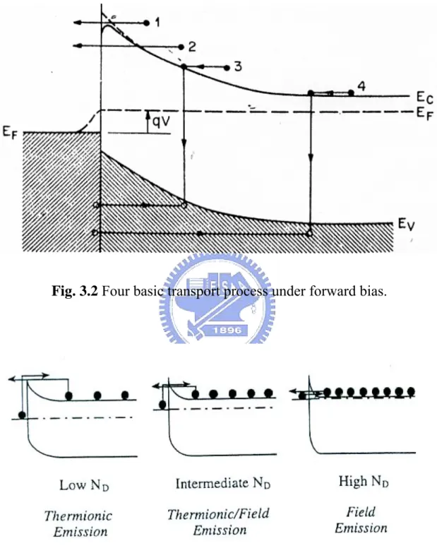
The current transport in metal-semiconductor contacts is mainly due to majority carriers, in contrast to p-n junction, where the minority carriers are responsible. Fig. 3.2 shows four basic transport processes under forward bias. The four processes are explains as following:
(1) Transport of electrons from the semiconductor over the potential barrier into the metal that the dominate process for Schottky diodes with moderately doped semiconductors such as Si with ND ≤ 1017cm-3
operated at moderate temperatures.
(2) Quantum-mechanical tunneling of electrons through the barrier height. This is important for heavily doped semiconductors and responsible for
most ohmic contacts.
(3) Recombination in the space-charge region (SCR) that identical to recombination process in a p-n junction.
(4) Hole injection from the metal to the semiconductor that equivalent to recombination in the neutral region [1].
With the SCR width being proportional to ND-1/2, it is obvious that highly
doped semiconductors have narrow SCR widths. For metal-semiconductor contacts with narrow SCR widths, electrons can to easy tunnel from the metal to the semiconductor and from the semiconductor to the metal. The conduction mechanisms for a metal to n-type semiconductor are illustrated in Fig. 3.3. For lowly doped semiconductors the current flows as a result of thermionic emission (TE) as show in Fig. 3.3(a) with electrons thermally excited over the barrier. In the intermediate doping range thermionic-field emission (TFE) dominates. The carriers are thermally excited to an energy barrier where the barrier is sufficiently narrow for tunneling to take place. For high doped densities, the barrier is sufficiently narrow at near the bottom of the conduction band for the electrons the tunneling directly, know as field emission (FE) [2].
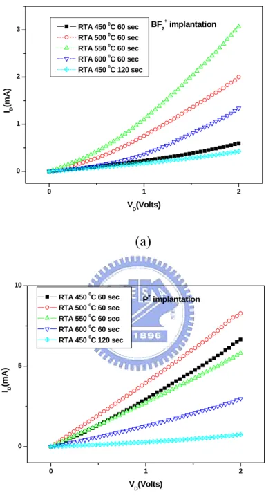
Fig. 3.4 shows the forward ID-VD characteristic curves of the NiSi/Si
junction diode with 2nd RTA 60 sec by (a) BF2+ implantation and (b) P+
implantation. We observe the activation of P+ implantation is more linear than BF2+ implantation, comparison between (a) and (b). Therefore, the P+
implantation curve presents the ohmic contact the linear curve to pass through 2nd RTA 60 sec. The forward currents rise along with the annealing temperature, nevertheless, after 550 ℃ and 500℃ maximize starts to reduce
along with the temperature rise for BF2+ and P+ implantation. According to
the extrapolation: NiSi/Si interface damage is recovered and roughness repaired at 500 ℃~550 ℃. This is assumes that as a result of the formation of dislocation above these temperature. In this temperature, forward bias currents are actually decreases. Some atoms that were already on substitutional site are believed to precipitate on or near these dislocations [3].
Fig. 3-5 shows ID-VD characteristic curves of the NiSi/Si junction diode
with 2nd RTA 60 sec by (a) BF2+ implantation and (b) P+ implantation. The
ID-VD characteristic curves approximate linear for P+ implantation. We knew
schottky contact turns ohmic contact after the annealing process. Fig. 3-6 Forward bias current density versus annealing temperature for the NiSi/Si junction diodes fabricated with (a) BF2+ and (b) P+ implantation at various
annealing time. Forward bias current density drops along with the time and the temperature rise. High thermal budget may promote interface state, causes the tunneling current is reduction [4-5].
3.2.2 Reverse leakage current density
Fig. 3-7 shows the reverse bias current density (JR) versus annealing temperature for the NiSi / Si junction diodes with an area of 0.0009 cm2 (300 × 300 µm) measured at a reverse bias of -2 V. The reverse bias current density (JR) is determined by directly dividing the measured current by the diode’s area. Roughness of the silicide/Si interface in a shallow junction may lead to the formation of localized Schottky contacts or the agglomeration-induced local silicide spiking, resulting in the increase of reverse bias current. After annealing at temperature above 550 60 sec℃
with BF2+ implantation, reverse bias currents are actually decrease. We
extrapolation the roughness of NiSi/Si interface related to junction leakages. With temperature rise the roughness of NiSi/Si interface is smoother, there is sufficient thermal budget to recovery defect and without agglomeration occur [6].
3.2.3 Current-Temperature measurement
We can obtain the activation level of M/S junction from current-temperature measurement. Fig. 3.8 and Fig. 3.9 shows the ID-VD
characteristic curves of the M/S junction diode with 2nd RTA 60 sec by BF2+
implantation and P+ implantation which measure temperature at 25, 45, 85 and 105℃, respectively. The BF2+ implantation curve presents the schottky
contact to pass through 2nd RTA 60 sec at room temperature measured. The schottky contact characteristic conversion to ohmic contact characteristic with measure temperature rise. For RTA 450 and 500℃ samples by BF2+
implantation, are tend to thermionic emission characteristic due to the current of M/S junction is sensitive to temperature. About RTA 550 and 600℃ samples by BF2+ implantation are trend to filed emission
characteristic. The current of P+ implantation samples are insensitive to temperature, therefore, have ohmic contact characteristic besides RTA 450℃ sample.
3.2.4 C-V measurement
The capacitance-voltage (C-V) technique relies on the fact that the width of a reverse-biased space-charge region (SCR) of a semiconductor junction device depends on applied voltage. This SCR width dependence on voltage
lies at the heart of the C-V technique. The C-V profiling method has been used with Schottky barrier diodes, p-n junction, MOS capacitance, and MOSFETs.
In this experiment, the results is not good to C-V measurement for us expect, however, other samples (as shows as Fig. 3.10.) can reach this expectancy which NiSi were implanted with BF2+/P+ ions at an energy of 20
and 10 k eV to a dose of 1×1013 cm-2. We extrapolation is capacitance of measure to bulk region for not good samples. In other words, N+N/P+P junction is so abruptness that depletion region occur near MS junction, consequently to measure C-V is not linear on reverse bias. Although we lack data of C-V measurement to estimation junction activation level, but only to know the different characteristics of I-V measurement with different 2nd RTA temperature should be contributed to the different in contact resistance. And P+ implantation samples shows more like ohmic contact behaviors than BF2+ implantation samples.
3.3 References
[1] S. M. Sze, Physics of Semiconductor Devices, 2nd ed., John Wiley &
Sons, Taipei, (1981).
[2] D. K. Schroder, Semiconductor Material and Device Characterization, 2nd ed., John Wiley & Sons, (1998).
[3] S. Wolf, and R.N. Tauber: “Silicon processing for the VLSI era”, second edition, Lattice press, Vol. 1, Chapter 10, 2000.
[4] F. Deng, R. A. Johnson, P. M. Asbeck, S. S. Lau W. B. Dubbelday T.Hsiao and J. Woo, J. Appl. Phys. 81, 8047, (1997).
[5] J. Chen, J. -P. Colinge, D. Flandre, R. GIllon, J. P. Raskin, and D.Vanhoenacker, J. Electrochem. Soc. 144, 2437, (1997).
[6] B. S. Chen and M. C. Chen, IEEE Trans. Electron Devices 43, 258, (1996).
Chapter 4
Electrical Characteristics of NiSi/n
+p, NiSi/p
+n ultra shallow
Junction Using Implant Into Silicide.
4.1 C-V Measurement
4.1.1 C-V Measurement Introduction
The effective dopant activation estimated that silicide dopant segregation
and pile-up at interface by capacitance-voltage (C-V) measurement. The measured capacitance was made up through three different capacitances in series, contain silicide/silicon junction capacitance, P-N junction depletion capacitance and backside contact capacitance. In silicide/silicon junction capacitance part, base on chapter three we can know where more likely to ohmic contact behavior. Consequently, we think that have high dopant concentration in silicide/silicon interface result in large capacitance. Let us can neglect the silicide/silicon capacitance in our analysis. About backside contact capacitance part, because of the area of contact is occupy wafer size which is larger than P-N junction area, therefore we also neglect backside contact capacitance term in our analysis [1]. As a result, the mainly measured capacitance was depletion capacitance and the model was shows in Fig. 4.1. The depletion-layer capacitance per unit area is defined as Cj =
dQ/dV, where Qis the incremental depletion charge on each side of the junction upon an incremental charge of the applied voltage dV [1]. For
one-side abrupt junctions, the capacitance per unit area is given by:
)
q
2kT
-(
2
C
V
V
N
q
W
bi B s s j−
=
=
ε
ε
(1)where V is positive/negative for forward/reverse bias. Rearrange the above Eq.(1): B s bi j
q
N
q
kT
V
V
ε
)
2
(
2
C
1
2−
−
=
(2)It is clear from Eq.(2) that by plotting 1/C2 versus V, a straight line should result from a one-sided abrupt junction as shows in Fig. 4.2. The slope gives the impurity concentration of the substrate (NB), and 1/C =0 gives
(Ψ
B
2
bi-2kT/q). Rearrange the above Eq.(2), we can obtain impurity
concentration at depletion layer edge.
]
)
/
1
(
[
q
2
(W)
N
2 s BC
d
dV
ε
=
(3) We know Ψbi equation: 2ln
i D A bin
N
N
q
kT
=
ψ
(4)Rearrange the above Eq.(4) which we can obtain the interface doping density can be estimate as following [2]:
kT q D i
e
biN
n
/ 2 AN
=
ψ for N-type (5) or kT q A ie
biN
n
2 / DN
=
ψ for P-type (6)4.1.2 Result and Discussion of C-V
The substrate doping density can be obtained from the different C-V data. We used Eq.(3) to plot the relationship between depletion capacitance and reverse bias voltage as shows in Fig. 4.3, and the building voltage of N+/P and P+/N junction can be obtained from 1/C2-V curve where 1/C2=0 as shows in Fig. 4.4. From linearly 1/C2-V curve implies that the linear abruptness junction is obtained. The results combined Eq.(3), Eq.(5) and Eq.(6) to estimate the doping density of N+/P and P+/N interface from average substrate doping density and building voltage as shows in Fig. 4.5 [3]. About above the results, at temperature above 500℃, doping density and building voltage of N+/P and P+/N interface are decrease with the temperature rise. The results were not conformed to us expect. Because the C-V measurement was measure the N+/P and P+/N junction interface, therefore, the junction interface went away from M/S junction interface with the annealing temperature increase as shows in Fig. 4.6. Moreover, the doping concentration was started to activation from the pile-up interface of MS junction. The measured result would exhibit the junction interface characteristic so that the higher temperature annealing showed the lower doping density.
4.2 I-V Measurement
4.2.1 I-V Measurement Introduction
For analyze the junction forming behavior, I-V measurement are adapted. The measuring sweep voltage was from forward bias to reverse bias for N-sub and P-sub samples. From the I-V curve, we could estimate the ideal factor by:
⎥
⎥
⎦
⎤
⎢
⎢
⎣
⎡
−
=
I
1
I
kT qV se
η (7)Rearrange the above Eq.(7):
⎥
⎥
⎦
⎤
⎢
⎢
⎣
⎡
=
kT qV se
ηI
I
as qV >> ηKT (8) or ) (ln J V kT q n ∂ ∂ = (9)Where η is called the ideality factor. The value of η is close to 1, when the forward current is dominated by diffusion current and is close to 2 when forward current is dominated by depletion recombination current. When both the diffusion current and recombination current are similar, the η is between 1 and 2.
4.2.2 Result and Discussion of I-V
The ideality factor can be determined from the slope of the linear segment of the I-V curve plotted on semilogarithmic coordinates [4]. The current range took to between 0.4 and 0.04 for N-sub samples which were between -0.4 and -0.04 for P-sub samples. The ideality factor of N+/P and P+N junction are exhibited in Fig. 4.7. The ideal factor would be affected by below factors: (1) contact resistance (2)generation-recombination current (3) substrate series resistance (4) high level injection. For the contact resistance, because high activation in junction, the MS interface would conversion from schottky contact to ohmic contact. For series resistance, cross to IR voltage bias of neutral region usually is smaller than KT/q so that can neglect this factor. And take current range does not the high level injection region so this does not dominate reason. We extrapolate the dominated factor might be due to defect induce generation-recombination current.
The on-off ratio as Jon (at VF = 1V) and Joff (at VR = 2V) of N+/P and P+N
diode are exhibited in Fig. 4.8. The reverse bias current is the minimum at 2nd RTA 450℃ 60s and 500℃ 60s treatment for N-sub and P-sub samples. Because exist defects in NiSi/Si interface result in higher reverse bias current. The defects may be derive from NiSi/Si interface (amorphous region) where is not entire recrystallized due to low thermal budget or low activation like at 2nd 450℃ for P-sub samples. With increasing 2nd RTA temperatures, the SPER process continuous going, and the Joff currents decreased, but
SPER process is completely at 2nd RTA 450℃ and 500℃ 60s treatment for N-sub and P-sub samples. The point of SPER process is completely to hold the most high on/off ratio. Although, the forward bias current is not mainly
factor for on/off ratio, but can be observed by the relative ideality factor which has the minimum ideality factor due to the forward bias is dominated by the diffusion current. After SPER is finished, with increasing 2nd RTA temperature, the reverse bias current will be reduces. The defect induce this results, due to SPER would be activation to a level above the equilibrium solid solubility during crystalline regrowth. While provide more thermal budget would be some atoms that were already on substitutional site are believed to precipitate on or near these dislocations after super-saturation. Another may be reason, dislocations start to form at the temperature range from 500 to 600℃ [5], itself or by some defect induced dopant deactivation at the P+/N and N+/P interface. The reverse bias current is mainly factor to affect on/off ratio at RTA temperature 550℃ to 600℃ for BF2+ implantation,
as show in Fig. 4.8(a). We extrapolation the defects start to dissolve in EOR regime at RTA temperature 600℃, result in the reverse bias current to drop. Another possible reason, because the behavior of junction is trend to Schottky-like region with doping layer width decrease under the fixed dopant concentration. Therefore, the reverse bias current will reduce due to the behavior is trend to PN-like at RTA temperature 600℃.
The current of PN junction was determined by minority carrier diffusion. However, the current of Schottky barrier diode was determined by thermionic majority carrier overcome potential barrier. The typical of generation current density of silicon PN junction is approximately 10-7 A/cm2, nevertheless, this is less than that of 2-3 order for the reverse current density of Schottky barrier diode, as shows as Fig. 4.9. In addition, threshold voltage of Schottky barrier diode is less than that of PN junction, as shows as Fig. 4.10 and Fig. 4.11. We clearly to know have Schottky barrier diode
characteristic with low energy and dose of ion implantation, due to high energy and dose of ion implantation to cause amorphous silicon region to deepen.
4.3 Activation Energy Measurement
The temperature dependence of reverse junction current IR can provide
insight into the leakage mechanism. The temperature dependence of reverse current IR is given by ) / exp( T IR ∝ 3 −Ea kT (10)
Where Ea is activation of the junction, k is the Boltzmann constant, and T is
the temperature at measurement. The value of Ea can be extracted from the slope of the semilogarithmic plot of log(IR/T3) versus 1000/T. The value of
Ea is close to the bandgap of silicon Eg when the reverse current is
dominated by the diffusion current and will be close to Eg /2 when the
reverse current is dominated by the generation current [6].
Fig. 4.12 shows the Arrhenius plots for the NiSi/P+N and NiSi/N+P junction fabricated by BF2+ implantation and P+ implantation. The
measurement was conducted at 2V reverse bias. Fig. 4.13 shows the activation energy of NiSi/ P+N and NiSi/N+P junction versus RTA temperature. We can observe Ea is close to Eg at the SPER process is
completely (450℃ for N-sub, 500℃ for P-sub samples) among all samples, which the reverse current is dominated by minority carrier diffusion current. After the SPER is finished, the Ea is reduces with the temperature increase,
and the reverse current is dominated by generation current. Compare Fig. 4.8 and Fig. 4.13, can to explain before extrapolation: because some atoms hold sufficient thermal budget that were already on subsitiutional site are to precipitate induce defects after super-saturation. The defects may be derive from amorphous region where is not entire recrystallized due to low thermal budget or low activation like at 2nd 450℃-500℃ for P-sub samples.
4.4 References
[1] K. M. Chang, J. H. Lin, C. H. Yang: accepted to the Fifth International Symposium on Control of Semiconductor Interface, (2007).
[2] S. M. Sze, Physics of Semiconductor Devices, 3rd ed., John Wiley & Sons, Taipei, (2007)
[3] C. H. Yang, “Research of Dopant Activation at the Interface between Nickel Silicide and Silicon during Nickel Silicide Formation”, NCTU(2007).
[4] C. C. Wang, Y. K. Wu, W. H. Wu and M. C.Chen, Japanese Journal of Applied Physics, Vol. 44, No 1A, 2005, pp. 108-113.
[5]S. Wolf, and R.N. Tauber: “Silicon processing for the VLSI era”, second edition, Lattice press, Vol. 1, Chapter 10, 2000.
[6] B. S. Chen and M. C. Chen, IEEE Trans. Electron Devices 43, 258, (1996).
Chapter 5
Conclusions and Future Work
In this thesis, we have been investigated the activation of B and P implant into silicide (IIS) by RTA process. With the device scale down, the shallow junction would be important because shallow junction formation can effectively suppress short channel effect (SCE). P+ implantation samples shows more like ohmic contact behaviors than BF2+ implantation samples
about P+/P and N+/N junction. Based on the IIS dopant segregation pile-up at interface and SPER, our experiment would achieve the high dosage activation and using low temperature annealing, and combine the I-V and C-V measurement to know SPER behavior of IIS method. We could find the best recipes for the device fabrication in the future. After SPER process finished, samples may cause defect formation and dopant deactivation phenomenon with higher thermal budget treatment above 450 and 500℃. With increasing 2nd RTA temperatures, the SPER process continuous going, and the Joff currents decreased, but SPER process is completely at 2nd RTA
450℃ and 500℃ 60s treatment for N-sub and P-sub samples. The point of SPER process is completely to hold the most high on/off ratio among all samples in this study. All in all, we achieved our purposes by means of the experiment and the results were beneficial.
In order to improve the shallow junction properties, we could make some
experiments to revise it in the future. We could use Spreading Resistance Profiling (SRP) to check the junction depth and the doping density. According to the actuality junction depth, we could also know that our fabricated junction does conform to the shallow junction condition or not. In
addition, we could also find the optimum value of annealing temperature. As long as the doping activation density and leakage current can attain our expectation at low annealing temperature, we can replace the high temperature fabrication.
Fig. 1.1 Continuation of Moor’s Law from intel’s high-k/metal gate
announcement (2003)
Fig. 1.2 Schematic of issue associated with silicide process.
Resistivity (μΩ-cm) Silicidation Temperature ( )℃ Silicon Consumption Moving Species Film Stress (dyn/cm2) 1.5×10¹⁰ TiSi2 12-15 800-950 0.9× T Si CoSi - 375-500 0.91× T Si - 1.2×10¹⁰ CoSi2. 18 550-900 1.04× T Co 6×10⁹ NiSi 15-16 350-700 0.82× T Ni NiSi2 35-50 700-850 - Ni -
T stands for thickness of silicide formed
Fig. 1.3 With/without bridging phenomenon of metal silicides.
P-type / N-type (100) Si sub.
z RCA clean
P-type / N-type (100) Si sub.
SiO2 300nm z Thermal Wet Oxidation
300nm
P-type / N-type (100) Si sub.
SiO2 SiO2 z Define active area region
(300μm x 300μm)
-z Ni film 20nm deposited by E-gun
P-type / N-type (100) Si sub.
SiO2 SiO2 z Silicidation by 1st RTA (400℃ 30s) z Selectively etch (H2SO4 : H2O2 = 3 : 1 ) 45 sec for unreact Ni
P-type / N-type (100) Si sub.
SiO2 SiO2
NiSi
z BF2 / Phosphorous ion
implantation
P-type / N-type (100) Si sub.
SiO2 SiO2
P-type / N-type (100) Si sub. PR SiO2 PR N+/P+ and P+/N+ NiSi
Ti SiO2 z Ti film 50nm deposited by E-gun
after coat PR next to remove PR. (lift-off)
z Coat TaN 150nm at backside by E-gun.
P-type / N-type (100) Si sub.
SiO2 SiO2
NiSi
N+/P+ and P+/N+
Ti
TaN 150nm
z Activation and junction formation by 2nd RTA (450 ~ 600℃) 60 sec
P-type / N-type (100) Si sub. SiO2 NiSi Ti N+/P+ and P+/N+ SiO2 44
-SiO2
Ti
Top View
Fig. 2.1 Process flow of P+/P, N+/N and P+/N and N+/P junction samples
of silicide contact for I-V and C-V electrical properties measurement.
Implanted ion 1st RTA 2nd RTA P substrate BF2+/20 keV/5E13 cm-2 PP + /20 keV/5E13 cm-2 400℃/60 sec 450 ~ 600℃ 60 sec N substrate PP + /20 keV/5E13 cm-2 BF2+/20 keV/5E13 cm-2 400℃/60 sec 450 ~ 600℃ 60 sec
Table 2.1 Process recipe of P+/P, N+/N and P+/N and N+/P junction by IIS
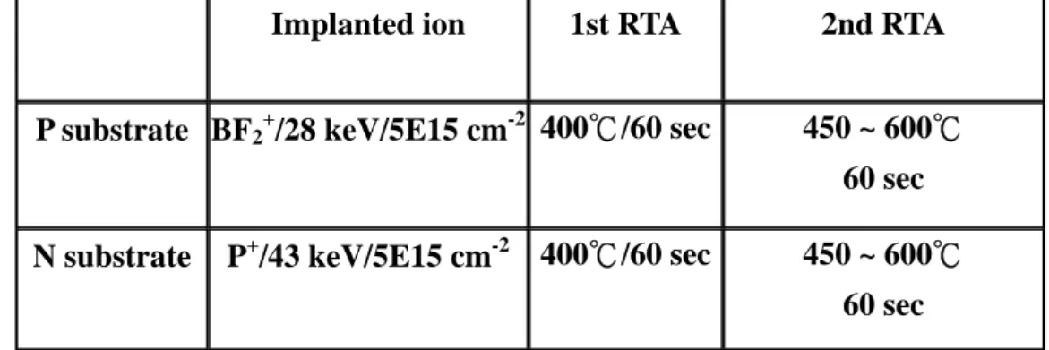
Implanted ion 1st RTA 2nd RTA P substrate BF2+/28 keV/5E15 cm-2 400℃/60 sec 450 ~ 600℃
60 sec N substrate PP
+
/43 keV/5E15 cm-2 400℃/60 sec 450 ~ 600℃ 60 sec
Table 2.2 Process recipe of P+/P, N+/N and P+/N and N+/P junction at
backside by IIS scheme.
-(a) (b)
(c) (d)
Fig. 3.1 AFM image shows NiSi/Si interface morphology by 2nd RTP
Fig. 3.2 Four basic transport process under forward bias.
Fig. 3.3 Depletion-type contacts to n-type substrates with increasing
doping concentrations. The electron flow is schematically indicated by the electrons and their arrows.
-0 1 2 0 1 2 3 BF2 + implantation ID (mA) VD(Volts) RTA 450 0C 60 sec RTA 500 0 C 60 sec RTA 550 0C 60 sec RTA 600 0 C 60 sec RTA 450 0C 120 sec (a) 0 1 2 0 5 10 P+ implantation ID (mA) VD(Volts) RTA 450 0 C 60 sec RTA 500 0C 60 sec RTA 550 0 C 60 sec RTA 600 0C 60 sec RTA 450 0C 120 sec (b)
Fig. 3.4 The forward ID-VD characteristic curves of the M/S junction
diode with 2nd RTA 30 sec by (a) BF2+ implantation and (b) P+
implantation.
-2 -1 0 1 2 -3 -2 -1 0 1 2 3 BF 2 + implantation ID (mA) V D(Volts) RTA 450 0C 60 sec RTA 500 0C 60 sec RTA 550 0C 60 sec RTA 600 0C 60 sec RTA 450 0 C 120 sec (a) -2 -1 0 1 2 -10 -5 0 5 10 ID (mA) V D(Volts) RTA 450 0C 60 sec RTA 500 0C 60 sec RTA 550 0 C 60 sec RTA 600 0C 60 sec RTA 450 0 C 120 sec P+ implantation (b)
Fig. 3.5 The ID-VD characteristic curves of the M/S junction diode with
2nd RTA 60 sec by (a) BF2+ implantation and (b) P+ implantation.