國 立 交 通 大 學
電子工程學系 電子研究所碩士班
碩 士 論 文
以鉿為基底之高介電常數閘極介電層之N通道金氧
半電晶體可靠度探討
Investigation of Reliability in Advanced Hf-Based High-k
Gate Dielectrics nMOSFETs
研 究 生 :曾友良
指導教授 :莊紹勳 博士
以鉿為基底之高介電常數閘極介電層之N通道
金氧半電晶體可靠度探討
Investigation of Reliability in Advanced Hf-Based
High-k Gate Dielectrics nMOSFETs
研 究 生 : 曾友良 Student : Yu-Liang Tseng
指導教授 : 莊紹勳 博士 Advisor : Dr. Steve S. Chung
國立交通大學
電子工程學系 電子研究所碩士班
碩士論文
A Thesis
Submitted to Department of Electronics Engineering & Institute
of Electronics College of Electrical and Computer Engineering
National Chiao Tung University
In Partial Fulfillment of the Requirements
For the Degree of Master
In
Electronics Engineering
July 2008
Hsinchu, Taiwan, Republic of China.
中華民國 九十七 年 七 月
i
以鉿為基底之高介電常數閘極介電層之N通道
金氧半電晶體可靠度探討
學生:曾友良 指導教授:莊紹勳博士
國立交通大學電子工程學系電子研究所碩士班
摘要
當元件氧化層持續微縮時,以二氧化矽為基底做為 CMOS 元件因
為閘極漏電流過高,無法滿足低功率電路的要求,故以高介電係數材
料取代二氧化矽是一個重要的課題。近年來在研究氮氧化鉿矽上,指
出可提高介電層物理厚度且有效降低閘極漏電流。與傳統的二氧化矽
或氮氧化矽閘極氧化層相比,以鉿為材料的高介電常數閘極介電層具
有相當嚴重的可靠度問題:臨界電壓漂移和操作電流的不穩定性,起
因於高介電材料層中有大量的缺陷,導致電荷捕捉與逃逸現象。所以
發展一套完整且可靠的方法去分析電荷捕捉的特性顯得相當重要。
本論文中,將以已發展成熟的「電荷幫浦」方法做為基礎,利用
操作頻率的不同來定性並定量的研究在介電層中缺陷分布的情形。通
道電子能穿隧的深度會隨著不同操作頻率而改變,因此可由電荷幫浦
電流對應到頻率便能得知在閘極介電層中不同深度的缺陷密度。
此方法用來觀察由製程造成閘極介電層缺陷,另外我們也研究在
ii
高介電層中嚴重的N通道元件正壓高溫破壞後的不穩定性。在不同操
作破壞條件下觀察缺陷產生情形,並將此結果與電性有效對應,如臨
界電壓、汲極電流等。藉由電荷幫浦方法,我們可以了解在不同製程
以及不同操作條件下介電層的良好程度,電路操作的可靠度問題,並
且對其物理機制有更深入的了解。
iii
Investigation of Reliability in Advanced Hf-Based
High-k Gate Dielectrics nMOSFETs
Student:
Yu-Liang Tseng
Advisors:Dr. Steve S. Chun
g
Department of Electrical Engineering & Institute of Electronics
National Chiao Tung University
ABSTRACT
With the aggressive scaling of CMOS devices, SiO2-based gate dielectrics can’t
conform the demand of low power application due to large gate leakage and high-k materials as the alternative of SiO2-based gate dielectrics has attracted a lot of interest.
Recently, the studies indicate that HfSiON dielectric significantly reduces gate leakage by increasing physical thickness. Compared to the conventional SiO2 or
SiOxNy gate dielectrics, Hf-based gate dielectrics are well known to suffer from the
serious reliability concern of threshold voltage shifts and operation current instability due to the fast charge trapping and de-trapping in the pre-existing bulk traps in high-k bulk layer. Therefore, it is very important to develop a integrated and reliable method to quantitatively characterize charge traps in high-k dielectrics.
In this thesis, proposed “Charge Pumping” approach is well developed and we will utilize it basically to study the traps distribution in dielectrics qualitatively and measurably. The available tunneling depth of channel carriers is dependent of frequency. Hence traps density in opposition to dielectric depth is extracted by charge pumping current and frequency.
iv
This method will be used to profile gate dielectrics traps induced by different process. Besides, positive bias temperature instable (PBTI) in high-k gate dielectric nMOSFETs is a critical issue and we will study it. In distinct stress condition, the traps generation will be powerfully related to characteristic in circuit level, such as threshold voltage and drain current. By charge pumping method, the quality and reliability of dielectrics in different process and distinct operation is distinguished and the physics behind is more understood.
v
誌 謝
在兩年碩士研究生涯中,首先要向我的指導教授莊紹勳老師表達深摯的謝 意。老師給予的課業上的指導與建議,讓我在學業與研究上獲益良多並學習到對 事物應有的嚴謹態度。除此之外,他對於學生的默默關懷,我必須在此表達感謝 之意。 感謝大正學長、耀賢學長、亞峻學長與元亨學長,在我在剛進研究所時, 不斷的給予我學業和操作儀器上的教導與協助,使我能在研究上無後顧之憂並且 很快上手。而在日常生活上,感謝那些和我一起嚐遍酸甜苦辣的同學,包括 zeky、易叡、文彥和建鴻,由於你們的相伴,原本枯燥的實驗也變的有趣,研究 上的艱辛與痛苦在與你們聊天下得到紓解,希望未來的日子裡,大家除了可以共 患難外亦可共享福。另外,對於汪老師研究群的學長:小馬學長、達達學長、志 昌學長亦懷有一份感恩的心,和你們在研究上的討論使我獲益良多,由於你們的 傾囊相授,使我在研究上得以順利解決困難。總歸一句,感念所有的夥伴,因為 你們的陪伴,使我兩年研究生活豐富,即使艱辛,仍充滿歡笑。 最後要感謝是我的家人,你們是我精神上最大的支柱,由於你們默默的支持 和關愛,我才能堅持下去。 謹將這份榮耀獻給培養我多年的父母親vi
Contents
Chinese Abstract
iEnglish Abstract
iiiAcknowledgments
vContents
viFigure Captions
viiiTable Captions
xiiChapter 1 Introduction
11.1 The Motivation of This Work 1 1.2 Organization of This Thesis 2
Chapter 2 Device Fabrication and Experimental Measurements
32.1 Introduction 3
2.3 Experimental Setup 4
2.3Device Fabrication 4
2.4 The Low Leakage IFCP Technique 7 2.4.1 Basic Theory 7 2.4.2 Experimental Setup of Charge Pumping Measurement 8 2.4.3 Principle of the Low Leakage IFCP Method 10 2.4.4 Application of the IFCP Measurement for High–K Dielectrics 13 2.5 Extraction of the Effective Channel Length 13 2.6 Geometry Effect in Charge-Pumping Measurement 16 2.7 Summary 18
Chapter 3 Investigation of the Properties in HfSiON Film
213.1 Introduction 21
3.2 Device Fabrication 22 3.3Extraction of the Traps in High-K Dielectrics 23 3.4 Depth Profiling of Traps in MOSFET with High-k Gate Dielectric 26 3.4.1 Basic Theory 26
3.4.2 Investigate Short Channel Effect in H-k Dielectric 27 3.5 Dielectric Degradation Phenomenon in nMOS High-k Devices
under Static PBTI Stress 28 3.5.1 Basic Theory 28
3.5.2 Charge Trapping and De-trapping Behaviors during Static PBTI
Stress 34 3.5.3 Result and Discussion 37
3.6 Summary 42
vii
4.1 Introduction 43
4.2 The Devices under Test 43
4.3 Results and Discussion 43
4.3.1 Comparison of halo B device before and after stress 43 4.3.2 Comparison of halo BF2 device before and after stress 54
4.3.3 Difference between halo B device and halo BF2 device 60
4.4 Summary 67
Chapter 5 Conclusion
71viii
Figure Captions
Fig. 2.1 The experimental setup and environment for basic I-V measurement of MOSFET’s…….5
Fig. 2.2 Schematic illustrations of device with different halo implant species. (a) Using
light atomic mass unit implant in halo B. (b) Using heavy atomic mass unit
implant in halo BF2………...6
Fig. 2.3 The experimental setup of charge pumping method………...9
Fig. 2.4 The schematic of charge pumping for (a) nMOSFET measurement. (b) pMOSFET
measurement. Induced leakage current (IG) occurs when tox < 20Å………..….11
Fig. 2.5 Measurement of ICP at two different frequencies. The low leakage IFCP method
is achieved by subtracting their respective ICP’s at two successive frequencies……….…12
Fig. 2.6 Illustration of ∆L0 extraction from C-P data. (a) Parameter definition and extraction
method. (b) Interface traps distribution in short and long channel length devices……...15
Fig. 2.7 (a) Non-uniform interface trap distribution for the extraction of effective channel
length. (b) To enlarge the figure to calculate ∆L0 ≈ 0.048µm……….16
Fig. 2.8 Charge-pumping measurement in short channel SiO2 gate dielectric NMOS device ...19
Fig. 2.9 Charge-pumping measurement of long channel SiO2 gate dielectric NMOS device…...20
Fig.3.1 (a) F=1MHz Charge-Pumping measurements. (b) F=10k Hz Charge-Pumping
Measurements…...24
Fig.3.2 The recombined charge per cycle (Qcp) for the high-k device. The charge-pumping
current is seen to increase for lower frequencies indicating that the charge pumping
ix
Fig.3.3 Volume densities of bulk traps in gate dielectric as a function of the distance from
Si surface……….………30
Fig. 3.4 Interface traps distribution in short and long channel length devices……….………31
Fig. 3.5 (a) The trap densities of different channel length devices at varied frequencies. (b) The
H-k dielectric trap densities of different channel length devices at varied frequencies….32
Fig. 3.6 Volume densities of bulk traps in gate dielectric of different lengths as a function
of the distance from Si surface………33
Fig. 3.7 Schematic band diagram of SiON/HfSiON gate stack for substrate injection. High
energetic electrons arrive at the anode………...….35
Fig. 3.8 (a) Low frequency (10kHz) Icp of with de-trapping and without de-trapping.
(b) High frequency (1MHz) Icp of with de-trapping and without de-trapping…………....36
Fig. 3.9 The measurement flow used to monitor the trap generation. Before each set of
charge-pumping measurements, a short non-stressing negative voltage is applies…..…..38
Fig. 3.10 (a) PBTI stress induces charge-pumping current varied. (b) Amplify the lower
frequencies charge-pumping current………..……….39
Fig. 3.11 (a) The trap densities of different temperature stress at varied frequencies. (b) The
high-k dielectric trap densities of different temperature stress at varied frequencies….…40
Fig. 3.12 Volume densities of bulk traps in gate dielectric of different temperature stress as a
function
of the distance from Si surface………..………..41
Fig.4.1 Delta threshold voltage of halo B device with positive and negative stress…………..….45
Fig.4.2 Drain current of halo B device versus gate voltage under different positive stress time....46
Fig.4.3 The drain current of halo B device under stress time of 2000 seconds after a left shift of
x
Fig.4.4 The change of drain current of halo B device versus gate voltage under different negative
stress time………..………..48
Fig.4.5 The subthreshold swing calculated by the slope of drain current curve in halo B
device………..49
Fig.4.6 The variation of interface trap density of halo B device in positive and negative stress
modes under different stress time……….………..51
Fig.4.7 The change of high-k gate dielectric trap density of halo B device in both stress modes
under different stress time………..……….52
Fig.4.8 The change of Gm,max of halo B device in positive and negative stress under different
stress time………..………..53
Fig.4.9 Delta threshold voltage of halo BF2 device with positive and negative stress…………...55
Fig. 4.10 Drain current of halo BF2 device versus gate voltage under different positive stress
time...56
Fig. 4 .11 The drain current of halo BF2 device under stress time of 2000 seconds after a left shift
of 0.088V will coincide with the curve of original device……….…………57
Fig. 4 .12 The change of drain current of halo BF2 device versus gate voltage under different
negative stress time……….………58
Fig. 4.13 The subthreshold swing calculated by the slope of drain current curve in halo BF2
device………..59
Fig. 4.14 The variation of interface trap density of halo BF2 device in positive and negative stress
modes under different stress time……….………..61
Fig. 4.15 The change of high-k gate dielectric trap density of halo BF2 device in both stress modes
under different stress time………..……….62
xi
stress time………..………..63
Fig. 4 .17 The off-state drain current of two different halo devices in different channel lengths
under VG=0V, VD=1.5V...64
Fig. 4 .18 Negative stressing induce delta Vt shift of the different halo implant…………..………..65
Fig. 4 .19 The subthreshold swing of different halo implant by negative stress under different stress
time……….………66
Fig. 4 .20 The band diagram during positive stress……….………...69
xii
Table Caption
1
Chapter 1
Introduction
1.1 The Motivation of This work
As the minimum feature size of CMOS devices continues to scale down, the SiO2 gate dielectric
meets its fundamental physical limits. To reduce the large gate leakage and maintain a low equivalent oxide thickness (OET), the gate dielectric materials with high dielectric constant (high-k) have been proposed to replace SiO2. [1,2]. However, most reports have shown that the use of high-k gate
dielectrics is apt to generate large number of interface traps at the surface channel and oxide trap charges in the gate dielectric bulk of MOS transistors, which would result in the degradation of device electrical characteristic [3–5].
The Qcp increase has been explained by the trap-to-trap tunneling process [6]. Charge-pumping
(CP) technique is known to be a very efficient tool for studying the traps in high-k gated dielectric. With the existence of border traps (high-k gated dielectric), it gradually increases as the frequency is lowered [7, 8]. A profiling technique based on the variation of Qcp with frequency was used to detect
the border traps near the high-k/Si interface and the interface traps [9]and to observe the phenomena and location of trap generation in the high-k dielectric bulk while constant voltage stress is applied.
Furthermore, during measurement, we need to overcome the induced leakage current using any of the above methods. It has been demonstrated successfully an IFCP (Incremental Frequency Charge Pumping) method for the interface characterization.
In this thesis, traps at various location of a stacked dielectric have been characterized by charge-pumping (CP) technique combined with multiple frequency measurement. Then we will
2
compare different halo implants devices by positive constant stress and negative constant stress. The excellent correlation of all types of traps to process conditions makes this method very promising for the applications in high-k dielectrics development.
1.2 Organization of this thesis
This thesis has been divided into five chapters. Chapter 2 describes the devices used in this work and experimental setup. The low leakage IFCP method for high-K dielectrics will be used to determine interface traps and the traps in high-K dielectrics. At the same time, the evaluation will be described. In Chapter 3, we will use the method of Chapter 2 to discuss varied channel length NMOSFETs with a polysilicon gate and HfSiON gate dielectric. In Chapter 4, we also use the same method to investigate the effect of halo implants species under stress polarity dependent constant voltage stress. Finally, a summary and conclusion will be given in Chapter 5.
3
Chapter 2
Device Fabrication and Experimental Measurements
2.1 Introduction
To reduce the high gate leakage, current major efforts are focused on replacing SiO2 and SiON
with high-k gate dielectrics. If a material with a dielectric constant larger than 3.9 of SiO2 is used, the
same equivalent oxide thickness ( EOT ) can be reached with a physically thicker layer. This ultimately leads to a reduction of the gate leakage current and allows further scaling of the gate oxide. The most promising candidate with sufficient high k-value is currently HfO2, but unfortunately there is an
interaction with the poly-Si gate, leading to Fermi level pinning, and large defect densities as well as VT instabilities are reported [4]. Only when metal gate electrodes are used, most of the unwanted
effects disappear and the poly-Si depletion can be eliminated. From integration point of view, poly-Si electrodes are still preferred and be used to speed up the introducing of high-k dielectrics. Hf-silicates ( HfSiON ) most likely will be the first to be introduced in integrated CMOS. Hf-silicates proved compatibility with poly-Si gate processing while maintaining good electrical characteristics. HfSiON can only be introduced if reliability is guaranteed [11]. However, the direct tunneling leakage is still large under EOT scaling down to below 16Å.
In order to analyze the reliability property of NMOSFET’s in thin HfSiON in the following chapters, we use a simple charge pumping method. As a result, the measurement setup and basic theory used are listed here. This chapter is divided into several sections. In the first section, the devices used in this study are examined. Then, the experimental analysis methods used in thesis will be introduced, including the low leakage IFCP method for high-k dielectrics.
4
2.2 Experimental Setup
The experimental setup for the I-V measurement of MOSFET’s is illustrated in Fig. 2.1. Based on the PC controlled instrument environment, the complicated and long-term characterization procedures for analyzing the intrinsic and degradation behavior in MOSFET’s can be easily achived. As shown in fig.2.1, the characterization equipment, including semiconductor parameter analyzer (HP4156C), dual channel pulse generator (HP8110A), low leakage switch mainframe (HP E5250A), cascade guarded thermal probe station and thermal controller, provides an adequate capability for measuring the device I-V characteristics. Besides, the PC program used to control all the measurement process is VEE and HT-basic.
2.3 Device Fabrication
MOS devices were fabricated based on advanced 90nm CMOS technology. The high K film deposited by ALD ( atomic layer deposition ) is HfSiON, while HfSiON films received post-deposition NH3 annealing. A given interfacial layer film was formed on a Si(100) wafer prior to high K film
deposition. Interfacial layer film used in this work is nitrogen-incorporated SiON. All wafers received HF cleaning prior to growing interfacial layer film. Halo B and halo BF2 are two different implant
5 HP 8110A Pulse Generator
Cascade Guarded Thermal
Probe Station Switch MatrixHP 5250A Parameter AnalyzerHP 4156
PC
Thermal Controller
HP 8110A Pulse Generator
Cascade Guarded Thermal
Probe Station Switch MatrixHP 5250A Parameter AnalyzerHP 4156
PC
Thermal Controller
6
Light Atomic Mass Unit
Heavy Atomic Mass Unit
IL(A)
(a)
HfSiON
IL(A)
(b)
HfSiON
Light Atomic Mass Unit
Heavy Atomic Mass Unit
Light Atomic Mass Unit
Heavy Atomic Mass Unit
IL(A)
(a)
HfSiON
IL(A)
(b)
HfSiON
IL(A)
(a)
HfSiON
IL(A)
(a)
IL(A)
(a)
HfSiON
IL(A)
(b)
HfSiON
IL(A)
(b)
IL(A)
(b)
HfSiON
Fig. 2.2 Schematic illustrations of device with different halo implant species. (a) Using light atomic mass unit implant in halo B. (b) Using heavy atomic mass unit implant in halo BF2.
7
2.4 The Low Leakage IFCP Technique
2.4.1 Basic Theory
The charging pumping principle for MOSFET’s has been applied to characterize the fast interface traps in MOSFET’s. The original charge pumping method was introduced by Brugler and Jespers, and the technique was developed by Heremans [12].This technique is based on a recombination process at the Si/SiO2 interface involving the surface traps. It consists of applying a constant reverse bias at the
source and drain, while sweeping the base level of the gate pulse train from a low accumulation level to a high inversion level. The frequency and the rise/fall time are kept constant. When the base level is lower than that flat-band voltage while the top level of the pulse is higher than the threshold voltage, the maximum charge pumping current occurs. This means that a net amount of charge is transferred from the source and drain to the substrate via the fast interface traps each time the device is pulsed from inversion toward accumulation. The charge pumping current is caused by the repetitive recombination at interface traps. As a result, the recombination current measured from the bottom (substrate) is the so-called charge pumping current [13]. The CP current can be given by:
ICP = q · f · W · L · NIT. (2.1)
According to this equation, the current is directly proportional to the interface trap density in the channel, the frequency, and the area of the device. However, when the top level of the pulse is lower than the flat-band voltage or the base level is higher than the threshold voltage, the fast interface traps are permanently filled with holes in accumulation or the electrons in inversion in n-MOSFET’s, which no holes reach the surface at the time, respectively. As a result, there is no recombination current and then the charge pumping current cannot be discovered.
8
Charge pumping measurements can be performed with several different ways. For our experimental requirement, we perform the charge pumping measurement by applying a gate pulse with the fixed base voltage (Vgl) and increasing the pulse amplitude. While the channel operates between
accumulation and inversion as the fixed base voltage lower than flat-band voltage and high voltage above the threshold voltage respectively; this gives rise to the charge pumping current (ICP) from the
bulk and reaches saturation situation. If we use another method which changes base voltage with fixed pulse amplitude, the current saturation region is not extensive enough for research because of the limit that the saturation current happens only when the gate pulse train from a low accumulation level to a high inversion level.
2.4.2 Experimental Setup of Charge Pumping Measurement
The basic setup of charge pumping measurement is shown in fig.2.3. The source, drain and bulk electrodes of tested devices are grounded. A 1MHz square pulse waveform provided by HP8110A with fixed base level (Vgl) is applied to NMOS gate, or with fixed top level (Vgh) is applied to PMOS gate.
We keep Vgl at –1.0V while increase Vgh from –1.0V to 1.0V by step 0.1V, or keep Vgh at 1.0V while
decrease Vgl from 1.0V to –1.0V by step –0.1V.
With a smaller voltage step, we get a higher profiling resolution. The parameter analyzer HP4156C is used to measure the charge pumping current (ICP).
9 Pulse GeneratorHP8110 n + n - n - n + P-substrate Vref HP4156 Pulse GeneratorHP8110 n + n - n - n + P-substrate Vref HP4156
10 2.4.3 Principle of the Low Leakage IFCP Method
Figures 2.4 (a) and (b) show the schematic of a low leakage IFCP measurement for CMOS developed by [14]. With both S/D grounded and by applying a gate pulse with a fixed base level (Vgl) and
a varying high level voltage (Vgh) for NMOS, the channel will operate between accumulation and
inversion. This gives rise to the charge pumping current ICP (=IB) measured from the bulk. However,
leakage current IG is unavoidable, as we see from Fig. 2.4 (a), the leakage of ICP is very small when tox
>30Å. However, it was revealed in Fig. 2.5 that the leakage current increases curves (1) and curves (2), for tested sample. From the measured ICP at two frequencies, ƒ1 and ƒ 2, can be expressed as :
ICP,ƒ 1 with-leakage= ICP,ƒ 1 correct + ICP,leakage@ƒ1 (2.2)
and
ICP,ƒ 2 with-leakage= ICP,ƒ 2 correct + ICP,leakage@ƒ2. (2.3)
When the frequency is sufficiently high, the leakage components in these two frequencies are almost the same (ICP,leakage@ƒ1 ≈ ICP,leakage@ƒ2 ). We then take the difference of ICP (∆ICP,ƒ 1-ƒ 2) between
two frequencies. From equations (2.2) and (2.3), the difference of these two CP curves gives :
11 Normal CP Curve Abnormal CP Curve (with AC leakage) (e.g., tox> 30A) (e.g., tox< 20A)
V
glI
CPI
CP,max Leak age componentvarying V
gl fixed VghI
BP
+P
+ N-subI
G Normal CP Curve Abnormal CP Curve (with AC leakage) (e.g., tox> 30A) (e.g., tox< 20A)V
ghI
CPI
CP,max Le akage componentvarying V
gh fixed VglI
BN
+N
+ P-subI
G(a)
(b)
Normal CP Curve Abnormal CP Curve (with AC leakage) (e.g., tox> 30A) (e.g., tox< 20A)V
glI
CPI
CP,max Leak age componentvarying V
gl fixed VghI
BP
+P
+ N-subI
G Normal CP Curve Abnormal CP Curve (with AC leakage) (e.g., tox> 30A) (e.g., tox< 20A)V
ghI
CPI
CP,max Le akage componentvarying V
gh fixed VglI
BN
+N
+ P-subI
G(a)
(b)
Fig.2.4 The schematic of charge pumping for (a) nMOSFET measurement, (b) pMOSFET measurement. Induced leakage current (IG) occurs
12 -1.0 -0.5 0.0 0.5 1.0 0.0 0.5 1.0 1.5 (3) (2) (1)
High Level Gate Voltage, V
gh(V)
Charge P
u
mp
ing Curren
t, I
cp(nA)
(3)=(2) - (1)
HfO2 NMOS W/L=10/1 um Icp,2MHz Icp,1MHz Icp,2MHz-1MHzFig.2.5 Measurement of ICP at two different frequencies. The low leakage IFCP method is
13
Since the correct CP curve is directly proportional to the frequency, it will be equal to the difference of two CP curves. Therefore, in the IFCP method, the correct CP curve at frequency (ƒ1- ƒ2) can be given by
ICP,ƒ 1-ƒ 2 = ∆ICP,ƒ 1-ƒ 2. (2.5)
For example, ICP(2MHz) - ICP(1MHz) is regarded as the ICP at their difference frequency, 1MHz. The
correct result is shown in curve (3).
2.4.4 Application of the IFCP Measurement for High–K Dielectrics
We mentioned that low leakage IFCP measurement can reduce the leakage component and extract interface state density accurately. Unfortunately this excellent method can not be applied to high K devices due to fast oxide traps. When a low frequency is applyied to gate, the ICP includes two
component which are ICP,Nit and ICP,Not. On the other hand, a high frequency applying to gate, the
composition of charge pumping current is almost Nit. This phenomenon has already been described by
R. Degraeve and A. Kerber [15]. Fig. 2.5 shows the charge pumping measurement at 1MHz and 2MHZ. We could found unreasonable results since ICP has two components at low frequency, if we applied the
IFCP measurement to high K device. In the meanwhile, we also find that high frequency CP measurement is more sensitive in gauging the interface state density. Using this characteristic, we improve IFCP for high K device.
2.5 Extraction of the Effective Channel Length
14
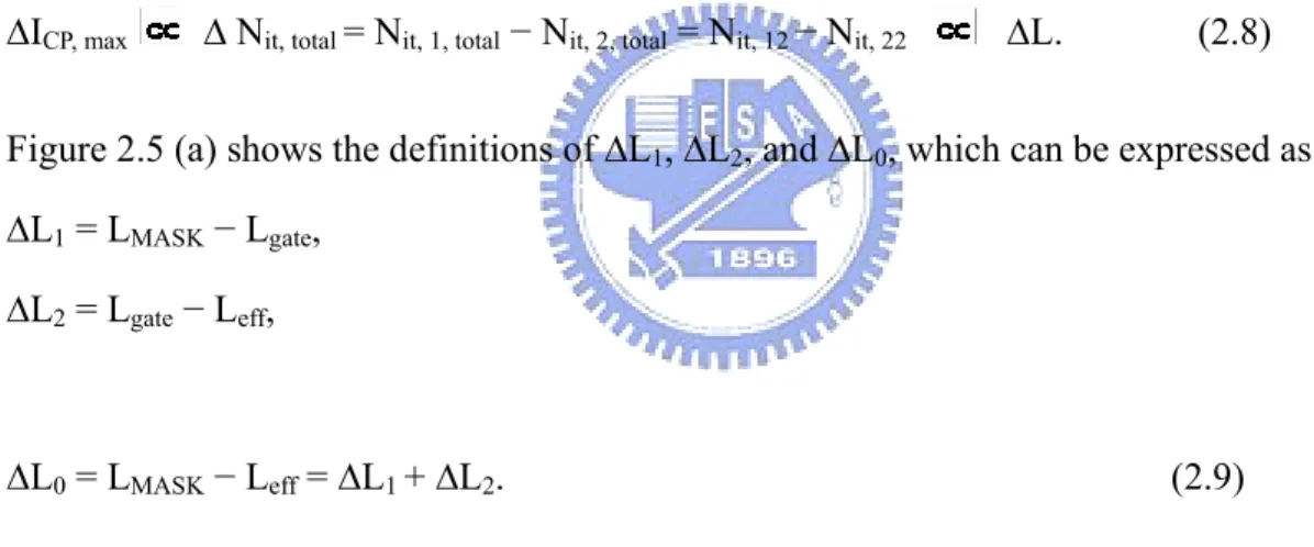
length. Using two different channel lengths, the interface traps can be represented by Nit, 1, total = Nit, 11(edge) + Nit, 12(center) (2.6)
and
Nit, 2, total = Nit, 21(edge) + Nit, 22(center). (2.7)
Since the mechanical stress in the edge region is more critical than the center region, the interface traps in the edge is larger than that in the center region and the mechanical stress in two different channel devices are almost the same, Nit, 11 is approximately equal to Nit, 21. To eliminate the traps
generated at the edge region, the difference of these two interface traps can be used, which is directly proportional to the ∆L. Hence, we have
∆ICP, max ∆ Nit, total = Nit, 1, total − Nit, 2, total = Nit, 12 − Nit, 22 ∆L. (2.8)
Figure 2.5 (a) shows the definitions of ∆L1, ∆L2, and ∆L0, which can be expressed as
∆L1 = LMASK − Lgate,
∆L2 = Lgate − Leff,
and
∆L0 = LMASK − Leff = ∆L1 + ∆L2. (2.9)
Figures 2.7 show the calculated interface traps, Nit, per unit width and offset length, ∆L0= LMASK −
Leff, from the measured 10 devices with two nMOSFETs in this work. Finally, we can get ∆L0=48nm
15
(a)
(b)
Nit,11 Nit,21 Nit,12 Nit,22(a)
(b)
Nit,11 Nit,21 Nit,12 Nit,22 Nit,11 Nit,21 Nit,12 Nit,22Fig.2.6 Illustration of ∆L0 extraction from C-P data. (a) Parameter definition
and extraction method. (b) Interface traps distribution in short and long channel length devices.
16 0.0 0.2 0.4 0.6 0.8 1.0 0 1x10⁷ 2x10⁷ 3x10⁷ 4x10⁷
Mask Length, LMASK
(
um)
In te rf ace T ra p p e r un it wi dt h-Nit *L
(
=ICP ,m a x / ( f* q *W ))
(#/cm)NMOS HfSiON Dielectric W=10um EOT= 10.7A
Halo B Halo BF2 0.0 0.1 0.2 0.3 0.4 0.5 6.0x10⁶ 1.2x10⁷ 1.8x10⁷
∆
L
0Mask Length, LMASK
(
um)
In te rf a ce Tra p pe r un it width-Nit *L
(
=ICP, m ax / (f *q*W))
( # /cm) NMOS HfSiON dielectric W=10um EOT= 10.7A Halo B
Halo BF2
Fig. 2.7 (a) Non-uniform interface trap distribution for the extraction of effective channel length. (b) To enlarge the figure to calculate ∆L0 ≈ 0.048µm.
17
2.6 Geometry Effect in Charge-Pumping Measurement
The charge pumping method is suitable for interface trap measurements on small geometry MOSFETs instead of large-diameter MOS capacitors. The MOSFET source and drain are tied together and slightly reverse biased with voltage VR. The time varying gate voltage is of sufficient amplitude for
the surface under the gate to be driven into inversion and accumulation. The charge pumping current is measured at the substrate, at the source-drain tied together, or at the source and drain separately. The interface traps, continuously distributed through the band gap, are represented by the four small horizontal lines at the semiconductor surface with the filled circles representing electrons occupying interface traps. When the gate voltage changes from positive to negative potential, the surface changes from inversion to accumulation. However, the important processed take place during the transition from inversion to accumulation and from accumulation to inversion.
When the gate pulse falls from its high to its low value during its finite transition time, electrons in the inversion layer shift to both source and drain. In addition, electrons captured by those interface traps near the conduction band are thermally emitted into the conduction band and also drift to source and drain. Those electrons on interface traps deeper within the band gap do not have sufficient time to be emitted and will remain captured on interface traps. Once the hole barrier is reduced, holes flow to the surface where some are captured by those interface traps still filled with electrons. Holes are indicated by the open circles on the band diagrams. Finally, most traps are filled with holes. Then, when the gate returns to its positive voltage, the inverse process begins and electrons flow into the interface to be captured. That meets a part of electrons flow into the inversion layer from the source and drain will not flow back into the source-drain. They would recombine with holes to generate charge pumping current. Nevertheless, under high frequency measurement, amount of carriers in channel center has not enough time to flow back into the source-drain as the channel is too long. That would induce a large current by recombine with holes through next state, accumulation mode. It will blight
18
wrong measured result. Fig.2.8 and fig.2.9 show the short and long channel SiO2 gate dielectric NMOS
in charge-pumping measurement. As the figures, long channel device has geometry effect to lead Icp to grow dramatically.
2.7 Summary
In this chapter, experiment analysis methods have been described. In the latter discussions, we will use these experimental techniques to discuss the traps in the gate dielectrics and interface trap in Si/IL (interfacial layer) for nMOSFET under stress polarity dependent constant voltage stress. By using the IFCP method and the method of separating Nit and Not, the difference between halo(B) and halo(BF2)
19 -0.5 0.0 0.5 1.0 0 100 200 300 400
SiO2 Dielectric NMOS
L=1um
W=10um Frequency = 1M
High Level Gate Voltage, V
gh(V)
C
h
arge Pumping Cur
rent, I
cp
(pA)
Fig.2.8 Charge-pumping measurement in short channel SiO2 gate dielectric
20 -0.5 0.0 0.5 1.0 0 10 20 30
High Level Gate Voltage, V
gh
(V)
Ch
arge
P
u
mp
in
g
C
u
rrent
, I
cp(n
A
)
SiO2 Dielectric NMOS
L=10um
W=10um Frequency =1M
Fig.2.9 Charge-pumping measurement in long channel SiO2 gate dielectric
21
Chapter 3
Investigation of the Properties in HfSiON Film
3.1 Introduction
Device scaling is a driving force of semiconductor industry in productivity and performance as predicted by Moor’s law. Nano-scale MOSFET transistor and MOS capacitor have reached their fundamental limits and the introduction of new gate dielectric materials has been surveyed and investigated for a continued scaling. As a trade-off for very short channel device length, ultra-thin and high quality gate oxide is strongly needed. Among them, high-K materials as a gate stack has attracted great interest. Recently, HfSiON has been successfully integrated into CMOS as gate dielectrics for low power applications, with good reliability and comparable mobility.
Threshold voltage (Vt) instability induced by charge trapping has been recognized as one of the
critical reliability issue in Hf-based high-k gate dielectrics, especially for nMOSFETs under positive bias stress [16]. In general, a defect band filled with plenty of pre-existing high-k traps is positioned above the Si conduction band edge in energy and in the HfSiON bulk layer in space [17]. In other words, these pre-existing high-k traps are distributed in a wide range of space and energy, thus making the charge trapping model different from that of SiO2. The high-k traps located at deep energy levels
are believed to responsible for the C-V hysteresis or Vt instability determined by static ID-VG
characteristics [3], [18]. And the high-k traps located at shallow energy levels are indicated as the physical origins of stress-induced leakage current (SILC) in HfSiON/IL high-k gate stacks [19]. In addition, the initial high-k bulk trap density has been demonstrated to be highly associated with the event of dielectric breakdown in HfSiON high-k gate dielectrics, thus influencing the device reliability and yield [15].
22
As reported in literatures, Si atoms could be in corporate into the HfSiON high-k gate dielectric to suppress the dielectric re-crystallization during high temperature rapid thermal annealing (RTA) and to reduce the high-k bulk trap density [20], [21]. Moreover, the thickness of base oxide (IL) plays a significant role in the charging and discharging dynamics of threshold voltage instability, and the tunneling time constant decreases exponentially with the decrease of base oxide thickness [22]. Although thin base oxide thickness is preferred for the continuous scaling of equivalent oxide thickness (EOT) below 1.0nm, this may further degrade the problem of threshold voltage instability due to fast charge trapping, Both the composition of high-k bulk layer and base oxide thickness are being modified to obtain the appropriate high-k gate stack structure with required EOT value and reduce threshold voltage instability.
Although, high-k dielectrics increase the physical thickness, the direct tunneling leakage still exists with EOT (equivalent oxide thickness) scaling down to below 16Å. Therefore, the leakage current will induce measurement error for ultra-thin gate dielectrics CMOS devices. To investigate the properties of HfSiON correctly, we need to eliminate the leakage current during the measurement by the IFCP method. The traps in the HfSiON and interface will be evaluated.
3.2 Device Fabrication
The devices used in this work were fabricated using 90nm CMOS technology. Test samples is nMOSFET which has halo implant with SiO2 and the effective oxide thickness is 10.7Å. Furthermore,
both of the high-k films is HfSiON with different halo implant species including light AMU and heavy AMU.
23
3.3 Extraction of the Traps in High-K Dielectrics
The technique of charge pumping is frequently used in the study of interface traps by applying a square wave to the gate of the device and measuring the resulting current through the source and drain. The interface traps charge and discharge with a charge pumping current (ICP) directly proportional to
frequency f; however, the charge recombined per cycle (QCP = ICP/f remains the same irrespective of the
measurement frequency [10]. In a device, with traps located spatially near Si/IL (interfacial layer) interface, is held in inversion for a period of time longer than the tunneling time constant, then communication may occur between the interface traps and traps in the high-K film. This results in an additional current component and gives rise to an increase of the charge recombined per cycle. In this work, devices fabricated with the HfSiON film are characterized by a high concentration of traps in the high-k film with a well-defined trapping distance, corresponding to the interfacial layer.
Because Icp is proportional to frequency so gate leakage would affect that at lower frequency. In
order to gat the accurate product, fig.3.1 shows the lowest (10k Hz) and biggest (1MHz) frequency Charge-Pumping measurements. Fig.3.2 shows the charge pumped per cycle (Qcp) as a function of
frequency ranging from 10k Hz to 1MHz. The objective of the latter definition is to eliminate the effects caused by the gate leakage and the tunneling dc currents from source/drain-to-gate overlap [23]. As can be seen in the figure, when the frequency is lower than 500k Hz (this frequency can be regarded as the break-point frequency), Qcp increases clearly with decreasing frequency.
The increase in Qcp can be attributed to the trap-to-trap tunneling of the border-trapped charges
close to the HfSiON/ interfacial layer andHfSiON bulk. As the frequency decreases to 10k Hz and lower, data does not show due to the large derivative disturbance resulted from noise signal.
24 -1.0 -0.5 0.0 0.5 1.0 0.0 2.0 4.0 6.0 8.0 10.0
High Level Gate Voltage, V
gh
(V)
C
harge Pum
p
ing Current,
I
cp(nA)
HfSiON NMOSFETEOT=10.7A Frequency=1M Hz W/L=10/1 um -1.0 -0.5 0.0 0.5 1.0 0.0 50.0 100.0 150.0Charge Pumpi
ng Current
, I
cp(pA)
High Level Gate Voltage, V
gh
(V)
HfSiON nMOSFET EOT=10.7A Frequency=10K Hz W/L=10/1 um(a)
(b)
-1.0 -0.5 0.0 0.5 1.0 0.0 2.0 4.0 6.0 8.0 10.0High Level Gate Voltage, V
gh
(V)
C
harge Pum
p
ing Current,
I
cp(nA)
HfSiON NMOSFETEOT=10.7A Frequency=1M Hz W/L=10/1 um -1.0 -0.5 0.0 0.5 1.0 0.0 50.0 100.0 150.0Charge Pumpi
ng Current
, I
cp(pA)
High Level Gate Voltage, V
gh
(V)
HfSiON nMOSFET EOT=10.7A Frequency=10K Hz W/L=10/1 um(a)
(b)
-1.0 -0.5 0.0 0.5 1.0 0.0 50.0 100.0 150.0Charge Pumpi
ng Current
, I
cp(pA)
High Level Gate Voltage, V
gh
(V)
HfSiON nMOSFET EOT=10.7A Frequency=10K Hz W/L=10/1 um(a)
(b)
Fig. 3.1 (a) F=1MHz Charge-Pumping measurements. (b) F=10k Hz Charge-Pumping measurements
25 10 100 1000 6.5x10⁻¹⁵ 7.0x10⁻¹⁵ 7.5x10⁻¹⁵ 8.0x10⁻¹⁵ 8.5x10⁻¹⁵ 9.0x10⁻¹⁵
Frequency (kHz)
C
h
a
rge R
e
co
mbin
ed per Cycl
e (I
cp/F)
HfSiON nMOSFET EOT=10.7A Frequency=10k to 1MHz W/L=10/1 umFig.3.2 The recombined charge per cycle (Qcp) for the high-k device. The charge-pumping current
is seen to increase for lower frequencies indicating that the charge pumping current is the sum of an interface trap component and a bulk trap in high-k dielectric.
26
Beside, at low frequency, nMOS exhibits significantly higher Nt. Such charge trapping in nMOS
not only reduces the amount of free carriers in the channel but also serves as additional coulomb scattering centers to lower the electron mobility. Nt of nMOS can be divided into two parts based on its
dependence on frequency: one is frequency independent part named as interface traps (Nit), which
locates at Si/IL interface next to channel with very short time constant. Another is frequency dependent part, which is referred to as oxide traps (Nhk) of the HfSiON layer. In this thesis, we will separate the
influence of the traps in HfSiON from the influence of interface traps on the charge recombined per cycle in a charge-pumping experiment. Since, by varying the charge-pumping frequency we can sense different fractions of the trap density. Therefore, using the above skill and the time constant of the electron trap-to-band tunneling detrapping process, it will help us to obtain the trap density in the HfSiON away from the interfacial layer.
3.4 Depth Profiling of Traps in MOSFET with High-k Gate Dielectric
3.4.1 Basic Theory
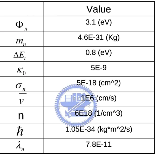
According to the model in [24], the extracted depth profile of border traps in the gate dielectric can be calculated by 1 ( ) ln( ) cp Hk m n t dQ N x qλ A E d f = − ∆ (3.1)
where A is the gate area, Qcp the charge pumped per cycle, f the measurement frequency,
/ 2 2
n mn n
λ =h Φ the attenuation coefficient, Φ the potential barrier, and n m the effective mass of n
electrons. The factor ∆ represents the energy gap in which traps will be allocated by electrons. The Et
rise/fall times of gate pulse in the CP technique of this paper are 10 ns. Such a transient time scans an energy gap of ∆ =Et 0.8eV[25]. In order to obtain the tunneling distance, x as a function of gate m
27 0 1 ln( ) m m n x t σ vn κ = (3.2)
where κ0 is the decay constant; κ0 =2 ,λn ≈tm 1/ 2f the tunneling time, σn the capture cross
section, v the thermal velocity, and n the carrier density. Table 3.1 lists the needed constants.
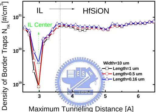
Fig. 3.3 shows the variation in the volume densities of bulk traps (Nhk) along the track of the
distance from Si surface. It can be seen that the Nhk density in the native oxide (≈ 1.5–3.7A) varied
rapidly near the HfSiON/IL. This is probably caused by the in-complete bonding near the interface [4], [27], [28]. We find a special point (xm ≈3A) that has the lowest trap density because it is center of IL.
A lot of studies have reported that traps in SiO2 are less than traps in HfSiON can prove above
phenomenon. In deeper depth (about 4–6.5 A), a uniform distribution of trap densities about 5*1020/cm3 is observed in the HfSiON bulk layer. This indicates that the bulk trap related reliability issues of high-k gated MOSFETs are the same as the formation of the HfSiON/IL interface.
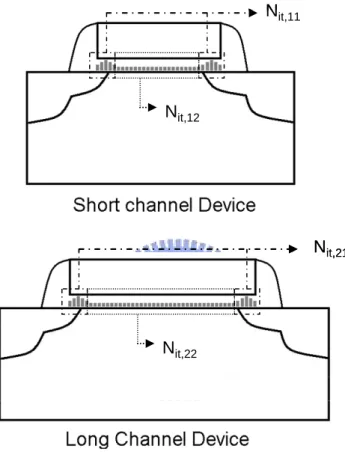
3.4.2 Investigate Short Channel Effect in H-k Dielectric
Fig.3.4 shows the interfacial traps distribution in short channel and long channel length devices. Since the mechanical stress in the edge region is more critical than the center region, the interface traps in the edge is larger than that in the center region. The relation can be distribute asNit,11 ≈ Nit,21,
it,12 it,11
N >> N , Nit,22 >> Nit,21. Fig.3.5(a) shows the trap densities of different channel length devices at varied frequencies. At lower frequencies, C-P measurement senses higher Nt. The flat region, higher
frequencies can be as Si/IL interfacial trap density. It is the same as we know that show channel length device has larger interface traps. The Si/IL interface traps of short channel devices (L=0.5 um and L=0.16 um) are more than long channel device (L=1 um). The increase amount of interface traps compared with L=1um are 14% and 20% in L=0.5um and L=0.16um respectively. Than we investigate high-k dielectric traps by Ncp minus Nit, it is the same as above concept. Fig.3.5(b) shows that. Fig.3.6
28
shows depth profiling of dielectric traps in different channel length devices. The lager Nhk occurs in
(IL/HfSiON) interface no matter different channel length. And all the points of lowest Nhk are about 3A.
It lets us believe that the point is interfacial layer center.
3.5 Dielectric Degradation Phenomenon in nMOS High-k Devices under Static
PBTI Stress
3.5.1 Basic Theory
Bias Temperature Instability (BTI) is a degradation phenomenon in MOS Field Effect Transistors (MOSFETs), known since the late sixties on SiO2 dielectrics. Even though the root causes of the
degradation are not yet well understood, it is now commonly admitted that under a constant gate voltage and an elevated temperature a build up of charges occurs either at the interface Si/SiO2 or in the
oxide layer leading to the reduction of MOSFET performances.
As a consequence of both the nitridation process step and the use of surface-channel devices, many researchers ascribed an accelerated BTI-like degradation of pMOSFETs under negative bias and elevated temperatures, the so-called NBTI (Negative Bias temperature Instabilities) effect [29], [30]. Unlike SiO2, the high-K dielectrics such as Hf-based dielectrics present serious instabilities for
negative and positive bias, after NBT and PBT (Positive Bias Temperature) stresses. The trapped charges are sufficiently high to represent one of the high-K integration's most critical showstopper. The instability is worrying, especially in the case of nMOS PBTI. In this section we present a review of process optimizations found in the literature. A new experimental methodology is also presented in order to asses with accuracy the real degradation and allows us to argue on possible PBTI mechanisms.
29
7.8E-11
1.05E-34 (kg*m^2/s)
6E18 (1/cm^3)
n
1E6 (cm/s)
5E-18 (cm^2)
5E-9
0.8 (eV)
4.6E-31 (Kg)
3.1 (eV)
Value
7.8E-11
1.05E-34 (kg*m^2/s)
6E18 (1/cm^3)
n
1E6 (cm/s)
5E-18 (cm^2)
5E-9
0.8 (eV)
4.6E-31 (Kg)
3.1 (eV)
Value
n
Φ
n
m
t
E
∆
0
κ
n
σ
v
h
n
λ
30 3 4 5 6 7 1019 1020 1021 HfSiON n-MOSFET W/L=10/1 um EOT=10.7A
Maximum Tunneling Distance [A]
De
nsi
ty of
B
o
rde
r T
rap
s N
hk[#/cm
3]
Fig 3.3 Volume densities of bulk traps in gate dielectric as a function of the distance from Si surface.
31 Nit,22 Nit,21 Nit,22 Nit,21 Nit,12 Nit,11 Nit,12 Nit,12 Nit,11
32 100 1000 4x10¹¹ 5x10¹¹ 6x10¹¹ 7x10¹¹
Trap Density =Icp/F/q/A Width=10 um Length=1 um Length=0.5 um Length=0.16 um
Tr
a
p De
nsity, N
cp(#/cm
2)
Frequency (kHz)
100 1000 0.0 5.0x10¹⁰ 1.0x10¹¹ 1.5x10¹¹Trap Density =Icp/F/q/A Width=10 um Length=1 um Length=0.5 um Length=0.16 um
Densi
ty of H-k Diel
ectri
c Trap N
Hk(#/
c
m
2)
Frequency (kHz)
(a)
(b)
100 1000 4x10¹¹ 5x10¹¹ 6x10¹¹ 7x10¹¹Trap Density =Icp/F/q/A Width=10 um Length=1 um Length=0.5 um Length=0.16 um
Tr
a
p De
nsity, N
cp(#/cm
2)
Frequency (kHz)
100 1000 0.0 5.0x10¹⁰ 1.0x10¹¹ 1.5x10¹¹Trap Density =Icp/F/q/A Width=10 um Length=1 um Length=0.5 um Length=0.16 um
Densi
ty of H-k Diel
ectri
c Trap N
Hk(#/
c
m
2)
Frequency (kHz)
(a)
(b)
100 1000 0.0 5.0x10¹⁰ 1.0x10¹¹ 1.5x10¹¹Trap Density =Icp/F/q/A Width=10 um Length=1 um Length=0.5 um Length=0.16 um
Densi
ty of H-k Diel
ectri
c Trap N
Hk(#/
c
m
2)
Frequency (kHz)
(a)
(b)
Fig. 3.5 (a) The trap densities of different channel length devices at varied frequencies. (b) The H-k dielectric trap densities of different channel length devices at varied frequencies.
33 3 4 5 6 1019 1020 1021 Width=10 um Length=1 um Length=0.5 um Length=0.16 um
Maximum Tunneling Distance [A]
Dens
ity
of B
o
rd
er T
raps N
hk[#/
c
m
3]
IL
HfSiON
IL Center
Fig 3.6 Volume densities of bulk traps in gate dielectric of different lengths as a function of the distance from Si surface.
34
3.5.2 Charge Trapping and De-trapping Behaviors during Static PBTI Stress
Fig. 3.7 shows the nMOS band diagram after stress, and the traps in HfSiON dielectric will capture electrons to induce more traps in HfSiON dielectric. However some electrons with lower energy may recover back into the cahnnel naturally. This would affect the measured result. In charge pumping measurement, too large gate voltage may increase trapping electrons and the negative low level bias may cause de-trapping. That would induce experimental error. Therefore we use one point charge pumping measurement to measure the traps change with stressing devices. In classic Icp curve,
we choose one point that high level gate voltage is higher than threshold voltage and low level gate voltage is lower than flat-band voltage to measure charge pumping current. This method can avoid the above issues in measurement. On the other hand, after stress we should de-trap by negative bias for ultra-small time. It can let the lower energy electrons de-trap more quickly.
Fig.3.8 shows the difference of stress process with de-trapping and without de-trapping. Charge pumping current of process with de-trapping is larger because the step lets electrons leave and produce more vacant traps to sense Icp.
35
SiON
Layer
High-k
Layer
V
G> 0 stress
SiON
Layer
High-k
Layer
High-k
Layer
V
G> 0 stress
Fig.3.7 Schematic band diagram of SiON/HfSiON gate stack for substrate injection. High energetic electrons arrive at the anode.
36 (a) -1.0 -0.5 0.0 0.5 1.0 0.0 50.0 100.0 150.0 200.0 250.0
Charge Pum
p
ing Current, I
cp(p
A
)
High Level Gate Voltage, V
gh(V)
F=10kHz W/L=10/1 um
Vg=2V stress 500 w/o detrapping Vg=2V stress 500 with detrapping
(b) -1.0 -0.5 0.0 0.5 1.0 0.0 5.0 10.0 15.0
High Level Gate Voltage, V
gh
(V)
Ch
ar
g
e
Pump
in
g Cur
ren
t, I
cp(nA)
F=1MHz W/L=10/1 umVg=2V stress 500 w/o detrapping Vg=2V stress 500 with detrapping
(a) -1.0 -0.5 0.0 0.5 1.0 0.0 50.0 100.0 150.0 200.0 250.0
Charge Pum
p
ing Current, I
cp(p
A
)
High Level Gate Voltage, V
gh(V)
F=10kHz W/L=10/1 um
Vg=2V stress 500 w/o detrapping Vg=2V stress 500 with detrapping
(a) -1.0 -0.5 0.0 0.5 1.0 0.0 50.0 100.0 150.0 200.0 250.0
Charge Pum
p
ing Current, I
cp(p
A
)
High Level Gate Voltage, V
gh(V)
F=10kHz W/L=10/1 um
Vg=2V stress 500 w/o detrapping Vg=2V stress 500 with detrapping
(b) -1.0 -0.5 0.0 0.5 1.0 0.0 5.0 10.0 15.0
High Level Gate Voltage, V
gh
(V)
Ch
ar
g
e
Pump
in
g Cur
ren
t, I
cp(nA)
F=1MHz W/L=10/1 umVg=2V stress 500 w/o detrapping Vg=2V stress 500 with detrapping
(b) -1.0 -0.5 0.0 0.5 1.0 0.0 5.0 10.0 15.0
High Level Gate Voltage, V
gh
(V)
Ch
ar
g
e
Pump
in
g Cur
ren
t, I
cp(nA)
F=1MHz W/L=10/1 umVg=2V stress 500 w/o detrapping Vg=2V stress 500 with detrapping
Fig.3.8 (a) Low frequency (10kHz) Icp of with de-trapping and without de-trapping. (b) High
37 3.5.3 Result and Discussion
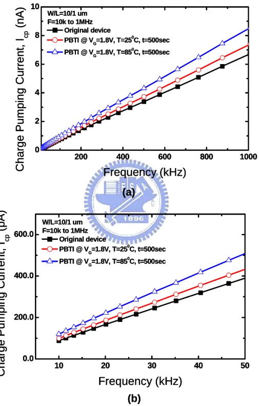
The schematic diagram of the stress and measurement sequence is shown in Fig.3.9. And fig.3.10 shows one point charge-pumping current varied after different PBTI stress. Charge pumping current is proportional to frequency high and low. No matter any frequencies, we can find the higher temperature has the large charge pumping current. That is because the higher temperature stress will induce more electrons to have enough energy to be charged in traps and bring more and more traps in high-k dielectric.
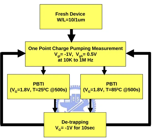
Fig.3.11 shows the trap densities as function of frequency measured on the original MOS device, after PBTI stress of different temperatures. The break point frequency found for original and after stressing devices, which is about 700kHz. Furthermore, the amount of trap density obtained for device after stressing is apparently higher than the original device. This indicates that a number of weak bounds hidden near the Si/high-k interface can be induced as border traps after stressing. And higher stress temperature would induce more trap density increase.
Fig.3.12 shows the volume densities of bulk traps in gate dielectric as a function of distance from Si surface, extracted from the trap densities versus frequency curves before and after different temperatures of PBTI stress. It can be seen that Nhk density in the dielectric bulk (~2.5-7.5A) has an
apparent increase after stress. However, the stress-induced bulk traps would more and more as stressing and burning stressing.
38
Fresh Device
W/L=10/1um
One Point Charge Pumping Measurement
V
gl= -1V, V
gh= 0.5V
at 10K to 1M Hz
PBTI
(V
G=1.8V, T=25
0C @500s)
PBTI
(V
G=1.8V, T=85
0C @500s)
De-trapping
V
G= -1V for 10sec
Fresh Device
W/L=10/1um
One Point Charge Pumping Measurement
V
gl= -1V, V
gh= 0.5V
at 10K to 1M Hz
PBTI
(V
G=1.8V, T=25
0C @500s)
PBTI
(V
G=1.8V, T=85
0C @500s)
De-trapping
V
G= -1V for 10sec
Fig. 3.9 The measurement flow used to monitor the trap generation. Before each set of charge-pumping measurements, a short non-stressing negative voltage is applies.
39 10 20 30 40 50 0.0 200.0 400.0 600.0
Charge Pumpi
ng Current
, I
cp(pA)
W/L=10/1 um F=10k to 1MHz Original device PBTI @ VG=1.8V, T=250C, t=500sec PBTI @ VG=1.8V, T=850C, t=500secFrequency (kHz)
200 400 600 800 1000 0 2 4 6 8 10Charge Pumping Curr
ent, I
cp(nA)
W/L=10/1 um F=10k to 1MHz Original device PBTI @ VG=1.8V, T=250C, t=500sec PBTI @ VG=1.8V, T=850C, t=500secFrequency (kHz)
(a)
(b)
10 20 30 40 50 0.0 200.0 400.0 600.0Charge Pumpi
ng Current
, I
cp(pA)
W/L=10/1 um F=10k to 1MHz Original device PBTI @ VG=1.8V, T=250C, t=500sec PBTI @ VG=1.8V, T=850C, t=500secFrequency (kHz)
200 400 600 800 1000 0 2 4 6 8 10Charge Pumping Curr
ent, I
cp(nA)
W/L=10/1 um F=10k to 1MHz Original device PBTI @ VG=1.8V, T=250C, t=500sec PBTI @ VG=1.8V, T=850C, t=500secFrequency (kHz)
(a)
(b)
Fig. 3.10 (a) PBTI stress induces charge-pumping current varied. (b) Amplify the lower frequencies charge-pumping current.
40 10 100 1000 4x10¹¹ 5x10¹¹ 6x10¹¹ 7x10¹¹ 8x10¹¹
Trap Densit
y, N
cp(#/
c
m
2)
W/L=10/1 um F=10k to 1MHz Original device PBTI @ VG=1.8V, T=250C, t=500sec PBTI @ VG=1.8V, T=850C, t=500secFrequency(kHz)
10 100 1000 0.0 5.0x10¹⁰ 1.0x10¹¹ 1.5x10¹¹ 2.0x10¹¹ W/L=10/1 um F=10K to 1MHz Original device PBTI @ VG=1.8V, T=250C, t=500sec PBTI @ VG=1.8V, T=850C, t=500secDensit
y of H
-k Diel
ect
ri
c
Trap N
hk(#/
cm
2)
Frequency (kHz)
(a)
(b)
10 100 1000 4x10¹¹ 5x10¹¹ 6x10¹¹ 7x10¹¹ 8x10¹¹Trap Densit
y, N
cp(#/
c
m
2)
W/L=10/1 um F=10k to 1MHz Original device PBTI @ VG=1.8V, T=250C, t=500sec PBTI @ VG=1.8V, T=850C, t=500secFrequency(kHz)
10 100 1000 0.0 5.0x10¹⁰ 1.0x10¹¹ 1.5x10¹¹ 2.0x10¹¹ W/L=10/1 um F=10K to 1MHz Original device PBTI @ VG=1.8V, T=250C, t=500sec PBTI @ VG=1.8V, T=850C, t=500secDensit
y of H
-k Diel
ect
ri
c
Trap N
hk(#/
cm
2)
Frequency (kHz)
(a)
(b)
Fig. 3.11 (a) The trap densities of different temperature stress at varied frequencies. (b) The high-k dielectric trap densities of different temperature stress at varied frequencies.
41 3 4 5 6 7 1020 1021
HfSiON
IL
IL Center
W/L=10/1 um F=10k to 1MHz Original device PBTI @ V G=1.8V, T=25 0 C, t=500sec PBTI @ V G=1.8V, T=85 0 C, t=500secD
e
n
sity of Bo
rd
er
T
raps N
bt[#/cm
3]
Maximum Tunneling Distance [A]
Fig.3.12 Volume densities of bulk traps in gate dielectric of different temperature stress as a function of the distance from Si surface.
42
3.6 Summery
In this chapter, we combine IFCP method and trap-to-band tunneling time constant to obtain trap position in the HfSiON. The IFCP method improves traditional charge pumping measurement by eliminating direct tunneling leakage current in ultra-thin gate dielectric films for MOS devices, and helps us to calculate more accurate traps in the HfSiON. On the other hand, we successfully separate Nit and Nhk with IFCP method for high-k dielectrics.
Using this method to investigate Nhk in different channel length devices and in different stress
condition, we find the break point frequency is similar at trap density versus frequency chart and IL center is fixed to the same point at Nhk versus the distance of trap position away from Si surface chart.
The results in this chapter show that there are more bulk traps existing in the high-k gate dielectric than in the SiO2 one. Experimental results indicate that the weak bonds present in high-k gate dielectric
are easily trapped by charges after stressing; thus, stress results in a large Vth shift. In addition, a novel
CP extraction technique has been proposed to measurement the spatial of the near-interface traps in the gate dielectric of high-k gated MOSFETs.