THURSDAY AFTERNOON
/
CLE0’98
/
413
190-zoo 0 1
introduced in a parallel JTC recognition system. It improved the discrimination tolerance signifi- cantly by using six times smaller pixel numbers of 25 X 25 as compared to the previous 64 X 64. The result ensures the throughput acceleration by increasing parallelism while keeping im- proved discrimination signal quality.
We thank M. Tsuchiya of the University of Tokyo for enlightening discussions.
*Japan Women’s University, Department of Mathematical and Physical Science, 2-8-1 Meji- rodai, Bunkyo-ku, Tokyo-1 12, Japan
1.
2.
3. 4.
5.
J.W. Goodman, Introduction to Fourier
Optics, 2nd ed. (McGraw-Hill, New York,
1996), Chapt. 8.
R. Thapliya et al., Proc. CLEO/Pacific Rim ’97 (IEEE/LEOS, 1997), paper FW4, pp. 3 10 -3 1 1.
R. Thapliya et al., Opt. Rev. 3, 397-399 (1996).
K. Kodate et al., Proc. CLEO/Pacific Rim ’97 (IEEE/LEOS 1997), paper FK3, pp. K. Kodate et al., Opt. Rev. 3, 400-402 (1996).
276-277.
CTh041
Miniature nonlinear optical-loop mirrors with semiconductor optical amplifiers Jinn-Haw Lee, Hsin-Jiun Chiang, Steffen Gurtler, C.C. Yang, College of Electvicd Engineering, National Taiwan
University, 1, Roosevelt Road, Section 4,
Taipei, Taiwan, R.O.C.; E-mail: jhlee@crlisajee. ntu.edu. tw
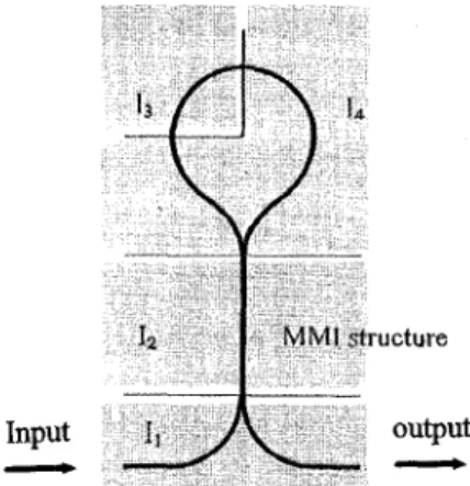
Nonlinear optical-loop mirrors are important devices for all-optical switching and other ap- plications. Typically, such a device consists of an optical fiber loop connected to a fiber cou- pler. The required optical nonlinearity may come from the Kerr effect in fiber or gain satu-
Input
-c
ructure
output
-
CTh041 Fig. 1. Layout of a miniature non- linear optical-loop mirror.
ration in an inserted semiconductor optical amplifier. Such a device with 1.5 m fiber loop length has a latency as large as 10 ns. In this paper, we present our experimental results of miniature nonlinear optical-loop mirrors made of GaAs/AlGaAs quantum-well optical amplifiers. The layout of such a device is shown in Fig. 1. The ridge-loading waveguide loop has a 300-pm radius with a 4-pm ridge width. The loop is connected to a multimode interference (MMI) waveguide 500 p m in length and 8 p m ridge width. Then the input
and output ports are also 4-*m waveguides with both lengths
-
100 bm. For injecting dif- ferent currents in different areas, we divided the electropad into four disconnected regions, indicated by the injection currents Il (input- output region), I2 (MMI region), I3 (one quar- ter of loop), andI4
(three quarters of loop). I3and
r,
are always different to break the symme- try of the two counterpropagating signals in the loop. The device shown in Fig. 1 should lead to a latency of 30 ps.The epitaxial structure of the semiconduc- tor optical amplifier consisted of five GaAs wells (6.5 nm in thickness) and four Al,,,,Ga, 75As barriers (20 nm in thickness), leading to a photoluminescence peak of -840 nm. To improve the quality of the curved waveguide in the loop so that the bending loss could be reduced, we used the cryoetching technique to etch the samples. With samples inside a chamber filled with C1, gas (-1 mTorr) and irradiated by a 193-nm excimer laser at a low temperature (-125 K), high- quality etching walls could be obtained. The etching depth was -1.8 pm, which reached the upper separate confinement layer. Figure 2 shows the top view of a finished device under a microscope.
Figure 3 demonstrates three sets of data shovving power-dependent switching. We launched a
cw
Tksapphire laser at 840 nm with various power levels and monitored the outputCThOll Fig. 2. Top view of a finished miniature nonliinear optical-loop mirror.
1
Output Coupler I1 = 55mA MMI I2 = 60mA
Output Coupler I1 = 55mA MMI I2 = 30mA
Output Coupler I1 = 27mA
0 10 20 30 40
Input Power(mW)
414
/
CLEO'98
/
THURSDAY AFTERNOON
power variation at the same wavelength. The horizontal axis in Fig. 3 shows the input power before entering the input waveguide. In this measurement, I3 = 350 mA,
I4
= 221 mA, and the other two injection currents are shown in the figure. All three curves show depression of output power when the input power reaches certain values. This is a typical power- dependent phenomenon observed in a nonlin- ear optical-loop mirror. Comparing the data sets of triangles and circles, we can see that different MMI injection currents, which lead to different coupling results, result in different switching threshold values. Meanwhile, a smaller input-output injection current leads to a larger switching threshold. From the data set of squares, we observe a contrast ratio 2.4 be- tween the outputs with inputs at 23 and 35 mW.CTh042
Ferroelectric-on-silicon modulators for high-density optical interconnects Feiling Wang, Dean Tsang, Hua Jiang, Kewen K. Li, Vladimir Fuflyigin, NZ Applied
Technologies, 8A Gill Street, Wobum, Massachusetts 01 801
The demonstration of a reflective optical modulator that can be integratedwith conven- tionally processed silicon wafers will be impor- tant for dense low-power optical interconnects to silicon complementary metal-oxide semi- conductor (CMOS) integrated circuits. Al- though ferroelectric-film-based optical modu- lators on silicon substrates were demonstrated,' the early work had no active silicon devices. We have successfully fabricated reflection-mode modulators on silicon wafers with active CMOS circuitry using a recently developed low- temperature technique for the growth of ferro- electric fdms on dielectric mirrors.
The ferroelectric modulator consists of a mirror/ferroelectric/rnirror thin film Fabry- Perot structure on a silicon wafer. A lead l m - thanum zirconate titanate (PLZT) material'
CThO42 Fig. 1. Photograph ofa silicon wafer with MOSFET devices on the left side and the ferroelectric thin-film modulators on the right side.
CThO42 Fig. 2. I-V characteristics of a MOS- FET after the modulator processing. Vertical scale, 0.1 mA/div.; horizontal scale, 1 V/div.; step generator, 1.0 V/div.
with ferroelectric relaxer properties was used as the tunable spacer. The optical length of the ferroelectric layer could be varied by an exter- nal electric field through a combination of the electrorefractive and electrostrictive proper- ties of the material. A moderate external field could increase the optical length of the PLZT layer by -1% and thereby modulate the re- flected light.
To prove the feasibility of using ferroelec- tric modulators for high-density free-space optical interconnects, we fabricated the modu- lators on silicon wafers with active CMOS cir-
from a MOSFET device after the modulator fabrication are qualitatively unchanged from the characteristics taken before modulator fab- rication. The onset voltage in the I-V curves, also observed before the modulator fabrica- tion, was believed to originate from a residual oxide layer in the MOSFET contacts. The func- tionality of the optical modulators was tested at a wavelength of 633 nm. The intensity modulation of the laser beam reflected from a 500 X 500 p m modulator on the wafer in response to a sinusoidal voltage signal is shown in Fig. 3.
PLZT materials possess inherently fast re- sponse speed.3 Calculations show that 5 ns switching speed is achievable in a 15 X 15 )*m modulator using CMOS drivers with 1 mA current. This demonstration of ferroelectric modulators fabricated on conventional CMOS is significant for high-density, low-power par- allel optical interconnects to and from silicon- integrated circuits.
F. Wang, G.H. Haertling, Conference
on
Lasers and Electro-optics, Vol. 15 of 1995 OSA Technical Digest Series (Optical So- ciety of America, Washington, D.C., 1995).
G.H. Haertling, Ferroelectrics 119, 51
( 1991).
C. Bao, J.-C. Diels, Conference on Lasers and Electro-Optics, Vol. 15 of 1995 OSA Technical Digest Series (Optical Society of America, Washington, D.C., 1995).
CTh043
Electro-optic effects in asymmetric coupled quantum wells
cuits and metal-oxide semiconductor field- ~
X. Chen, A. Bhatnagar, M.P. Earnshaw, effect transistor (MOSFET) test structures.
Before the fabrication of the modulators, the
I- Vcharacteristics of the MOSFETs were mea- sured. Reflection-mode modulators of various sizes were then fabricated on the silicon wafers. After completion of the modulators, the char- acteristics of the MOSFET devices were reex- amined, and functionality of the optical modulators was tested. Figure 1 shows a pho- tograph of the silicon wafer with the active MOSFET devices on the left side and the reflection-mode modulators on the right side. The I-Vcharacteristic curves (Fig. 2) taken
CTh042 Fig. 3. Light-intensity modulation detected from a reflection-mode ferroelectric modulator on a silicon CMOS wafer. Upper trace is the light intensity and lower trace is the applied voltage.
W. Batty,* D.W.E. &lsopp, Department of
Electrontcs, University of York, York, England YO1 5DD; E-mail xc2@ohm.york.ac.uk
Coupled quantum-well systems have been shown from calculations of electroabsorption and subsequent Kramers-Kronig transforma- tion to yield large refractive-index changes with applied electric field. 1-3 Such calculations
of refractive-index change in symmetric coupled double quantum wells (QWs) have been shown, by detailed comparison with ex- periment, to be sensitive to the model used? In this paper, we report a study of the electro- optic properties of a range of asymmetric coupled GaAs-Al,Ga,_,As QW (ACQWs)
based on a n accurate application of the exci- tonic Green's-function (EGF) method of Chuang et al?
The basic ACQW structure comprises a shallow, wider Al,Ga,_,As well separated from a deep, narrow GaAs well bya barrier that is sufficiently thin (typically -2 nm) to yield
.
strong coupling between the two wells. The large refractive-index change predicted by Susa' and Thirstrup' derives principally from a redistribution of oscillator strength between the elhhl and elhh2 transitions as the hhl (or e l ) and hh2 (e2) wave functions localize into QWs of different width and depth when an electric field is applied, while the e l (hl) wave function remains unchanged.Figur: 1 shows electroabsorption spectra for 60-A-wide Al,~,,Ga,~,,As well separated